Questions for Self-Testing
1. What registers are used to interact between the CPU and main memory?
2. What is the difference between a synchronous and an asynchronous transfer mechanisms?
3. How are addition and subtraction performed in a computer with one bus?
4. Why does the multiplication and division time exceed the time consumed by other instructions?
5. How is data interchange between the CPU and main memory organized?
1.3. Register Gating and Timing of Data Transfers
L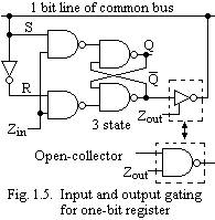 et
us consider the case where each bit of the registers in Figs 1.3 and
1.4 consists of a simple latch shown in Fig. 1.5. The shown storage
element is assumed to be one of the bits of register Z. While the
control input Zin
is equal to 1, the state of the latch changes to correspond to the
data on the bus. Following a 1 to 0 transition at the Zin
input, the data stored in the latch immediately before this
transition is locked in until Zin
is again set to 1. Thus the two input gates of the latch implement
the function of the input control switch in Fig. 1.4.
et
us consider the case where each bit of the registers in Figs 1.3 and
1.4 consists of a simple latch shown in Fig. 1.5. The shown storage
element is assumed to be one of the bits of register Z. While the
control input Zin
is equal to 1, the state of the latch changes to correspond to the
data on the bus. Following a 1 to 0 transition at the Zin
input, the data stored in the latch immediately before this
transition is locked in until Zin
is again set to 1. Thus the two input gates of the latch implement
the function of the input control switch in Fig. 1.4.
When a given switch is in the ON state, it transfers the contents of its corresponding register to the bus. When it is in the OFF state, it is electrically disconnected from the bus. That is, it does not put the bus in any specific state, thus allowing another register to place data on the bus. Hence the output of the register-switch combination can be in one of the three states 1, 0, or open circuit. That is, it is capable of being electrically disconnected from the bus. It is also able to place either a 0 or a 1 on the bus when needed. Because it supports these three possibilities, such a gate is said to have a three-state output. A separate control input is used to either enable the gate output or to put it in a high-impedance (electrically disconnected) state. The latter corresponds to the open-circuit state of a mechanical switch.
A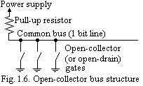 n
alternative design for the common bus of Fig. 1.4 that does not
require the output switches shown makes use of open-collector (for
bipolar) or open-drain (for MOS) gates. The output of such a gate is
equivalent to a switch to ground. The switch is open when the gate
output is in the 1 state and closed when it is in the 0 state. The
structure of an open-collector bus is represented symbolically in
Fig. 1.6.
n
alternative design for the common bus of Fig. 1.4 that does not
require the output switches shown makes use of open-collector (for
bipolar) or open-drain (for MOS) gates. The output of such a gate is
equivalent to a switch to ground. The switch is open when the gate
output is in the 1 state and closed when it is in the 0 state. The
structure of an open-collector bus is represented symbolically in
Fig. 1.6.
When idle, the bus is maintained in the 1 state by the "pull-up" resistor shown. Thus, as long as all gate output switches are open, that is, all outputs are in the 1 state, the bus remains in the 1 state. If any gate output changes to the 0 state, the corresponding output switch is closed, and the bus is "pulled down" to the 0 state. In other words, the bus performs an AND function on all gate outputs connected to it. Sometimes, this is referred to as a "wired-AND" connection. If this gating arrangement is used, an open-collector NAND gate as shown may replace the three-state output gate of Fig. 1.5. When Zout is high (1), the bit stored in the latch is fed to the bus. When Zout is low (0), the bus is left in the 1, or idle, state, allowing data from another register to be transferred to the bus. In general, the three-state design enables faster data transfers in comparison with the open-collector, or open-drain, approach. For this reason, it is much more commonly used in bus design. The main distinguishing feature of an open-collector bus is it’s wired-AND capability. Hence, the open-collector arrangement is used primarily for bus lines where this capability is needed.
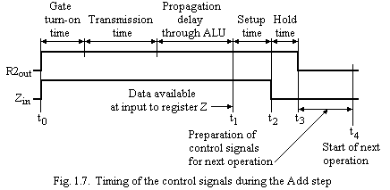
Let us now discuss some aspects of the timing of data transfers inside the CPU. From the time the signal R2out is set to 1, a finite delay is encountered for the gate to open and then for the data to travel along the bus to the input of the ALU. The ALU adder circuits introduce further delay. For the result to be properly stored in register Z, data should be maintained on the bus for an additional period of time equal to the setup and hold times for this register. This situation is depicted in the timing diagram given in Fig. 1.7. The sum of the five delay times shown defines the minimum duration of the signal R2out.