

Questions for Self-Testing
1. What is the annual rate of transistor count growth?
2. What does the fact that voltage tends to drop with each process improvement permit?
3. What is the conflict between technological and architecture requirements?
4. What are the tendencies in computer architecture evolution taking account of Moore’s law?
5. Why is connectivity a key element in the system architecture?
4.2. Stack Computers
Precision Architecture Computers. A commonly used technique is to dedicate one hardware register to serve as a stack pointer (SP) that contains the memory address of the top word in the stack. In addition, two stack instructions PUSH and POP are provided. The PUSH instruction causes data to be pushed onto the top of the stack. It specifies the address of this data, or perhaps the data itself. Conversely, the POP instruction transfers the top element on the stack into the location specified in the instruction. Of course, both PUSH and POP instructions update the contents of the SP automatically.
The capability of realizing a stack data structure in the main memory has become a common feature in modern computers. It is equally important in large and small machines. However, despite its importance, it is usually not the dominant characteristic of a typical computer.
There are a number of computational tasks where the stack data structure naturally leads to an efficient implementation. Indeed, a number of commercially successful “stack computers” have been developed. The best-known examples are the Burroughs Corporation’s line of computers: B5500, B6500, and B6700. These are large general-purpose computers. A notable example of a RISC stack machine is the Hewlett-Packard Company’s HP-computers, for example HP-8800 [13], [27], [43], [44], [50], [53], [60], [61], [62].
Let
us explore some possibilities for the organization of a stack
computer. Its key component is the stack. We already know that the
stack can reside in the main memory. An alternative may be to
implement a stack using a set of registers. Let us assume that a
stack capable of storing n-bit
words is needed. Furthermore, let the required capacity of the stack
be k
words.
Fig. 4.4,a
shows a configuration where k
registers, of n
bits each, realize the
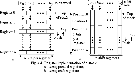 desired
stack. The registers are connected so that a Push signal transfers
the contents of all registers downward by one position; that is the
contents of register i
are transferred into register i
+ 1. The n-bit
word is pushed onto the stack by loading it into register 0.
Similarly, a Pop signal transfers the contents of all registers
upward by one position. Thus the contents of register i
are
transferred into register i
–
1. The original contents of register 0 are the n-bit
word popped off the stack.
desired
stack. The registers are connected so that a Push signal transfers
the contents of all registers downward by one position; that is the
contents of register i
are transferred into register i
+ 1. The n-bit
word is pushed onto the stack by loading it into register 0.
Similarly, a Pop signal transfers the contents of all registers
upward by one position. Thus the contents of register i
are
transferred into register i
–
1. The original contents of register 0 are the n-bit
word popped off the stack.
Another possibility is to use n shift registers, each of which has a capacity of k bits, as indicated in Fig. 4.4,b. The shift registers must have the capability of shifting their contents in either direction, one bit position at a time. Under a Push signal the ith word in the stack, which occupies the ith bit position in all n registers, is shifted into the (i + 1)st position. Bit position 0 is loaded with the n-bit word that is being pushed onto the stack. A similar operation is performed under the Pop signal. In this case, the contents in bit position 0 are shifted out of the register as the n-bit word is popped off the stack.
The main disadvantage of these schemes is the cost of the needed hardware. The stack depth k may be large (k > 1000), which implies the usage of either many relatively short n-bit registers, or considerably fewer long shift registers. In practice, neither of the above schemes has found much favor. The alternative of using the main memory to implement the stack remains the most cost-effective approach that is used in commercial stack computers. Such machines rely heavily upon a set of hardware registers, used as pointers to the stack in the memory. On the other hand, they do not normally contain general-purpose registers of the type found in conventional computers. To give the reader an idea of how a stack computer may be organized, we will consider a few of the features of HP-computer.
Stack Structure of the HP-Computer. The main memory contains the program instructions and the required data in separate domains. Instructions and data cannot be intermixed except for immediate data that may be used in the program. Hardware registers are used as pointers to the program and data segments as shown in Fig. 4.5. Three registers define the program segment. The program base (PB) and the program limit (PL) registers indicate the memory area occupied by the program. The program counter (PC) has the usual function of pointing at the current instruction. The contents of the data base (DB) register denote the starting location of the stack. The stack grows in the higher-address direction.
The
above pointer registers specify the existing size, the maximum size,
and the location in memory of the stack. Thus the stack is a dynamic
structure that can be easily changed. Fig. 4.5 shows one other
pointer that has not yet been discussed: the stack marker (Q)
register. It is used to denote the starting
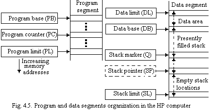 point
for the data of the current routine or “procedure.” Actually, it
points to the fourth word of a four-word entry in the stack, named
the stack marker, which facilitates passing of control between
procedures. Fig. 4.6 shows two stack markers, one corresponding to
the current procedure (Procedurek)
and another that is placed onto the stack when a new procedure
(Procedurek+1)
is initiated.
point
for the data of the current routine or “procedure.” Actually, it
points to the fourth word of a four-word entry in the stack, named
the stack marker, which facilitates passing of control between
procedures. Fig. 4.6 shows two stack markers, one corresponding to
the current procedure (Procedurek)
and another that is placed onto the stack when a new procedure
(Procedurek+1)
is initiated.
U pon
completion of the new procedure, control is transferred to the
pre-vious procedure by means of the data in the stack marker
k
+ 1. At that time, the Q register must be set to point at the fourth
word of the stack marker k.
This is readily accomplished, since the distance between the
stack markers is stored as a part of each marker. Also, the SP is
set to point at the location immediately preceding the stack marker
k
+ 1. Thus, the SP points at the top of the stack used by Procedurek.
This restores the situation that existed at the time when
Procedurek-1
was invoked. The technique described above can be used to nest any
number of procedures. Note that we have simplified our discussion by
leaving out the parameter-passing protocols, which also make use of
the stack.
pon
completion of the new procedure, control is transferred to the
pre-vious procedure by means of the data in the stack marker
k
+ 1. At that time, the Q register must be set to point at the fourth
word of the stack marker k.
This is readily accomplished, since the distance between the
stack markers is stored as a part of each marker. Also, the SP is
set to point at the location immediately preceding the stack marker
k
+ 1. Thus, the SP points at the top of the stack used by Procedurek.
This restores the situation that existed at the time when
Procedurek-1
was invoked. The technique described above can be used to nest any
number of procedures. Note that we have simplified our discussion by
leaving out the parameter-passing protocols, which also make use of
the stack.
S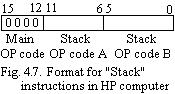 tack
Instructions. The
basic strategy in stack computers is to perform operations on the
data that is in the top few locations of the stack. This implies
that many instructions will use operands that are already in these
locations. Furthermore, the results generated are left on the stack.
Of course this assumes the existence of instructions that can move
data between the stack and other main memory locations. Next,
we will consider the “Stack” instructions, whose format is shown
in Fig. 4.7. This class of instructions is identified by four 0s in
the high-order bit positions.
tack
Instructions. The
basic strategy in stack computers is to perform operations on the
data that is in the top few locations of the stack. This implies
that many instructions will use operands that are already in these
locations. Furthermore, the results generated are left on the stack.
Of course this assumes the existence of instructions that can move
data between the stack and other main memory locations. Next,
we will consider the “Stack” instructions, whose format is shown
in Fig. 4.7. This class of instructions is identified by four 0s in
the high-order bit positions.
Forth Reduced Instruction Set Computer. Forth Reduced Instruction Set Computer (FRISC) is named after the Forth language, which was proposed by Charles Moore. The Johns Hopkins University / Applied Physics Laboratory (JHU/APL) FRISC-3 is a hardwired 32-bit processor optimized for executing the Forth programming language. The focus of the FRISC-3 is on single cycle execution of Forth primitives in a real time control environment. JHU/APL developed the FRISC-3 in response to their need for a fast Forth language processor for spaceborne control processing applications in satellites and Space Shuttle experiments. The primary use of the FRISC-3 is for embedded real time control, especially in spacecraft (which is the focus of the JHU/APL group), but also for other industrial and commercial applications. Fig. 4.8 is an architectural block diagram of the FRISC-3. The Data Stack and Return Stack are implemented as identical hardware stacks. They each consist of a stack pointer with special control logic feeding an address to a 16 element by 32 bit stack memory arranged as a circular buffer. The top four elements of both stacks are directly readable onto the Bbus. In addition, the topmost element of the Data Stack may be read onto the Tbus (Top-of-stack bus) and the topmost element of the Return Stack may be read onto the Abus (return Address bus). Both stack buffers are dual-ported, which allows two potentially different elements of the stacks to be read simultaneously. Only one stack element may be written at a time.
One
of the innovative features of the FRISC-3 is the use of stack
management logic associated with the stack pointers. This logic
automatically moves stack items between the 16-word on-chip stacks
and a program memory stack spilling area to guarantee that the
on-chip stack buffers never experience an overflow or underflow.
This logic steals program memory cycles from the processor to
accomplish this, avoiding the extra stack data pins on the chip in

exchange for a small performance degradation spread throughout program execution. The designers of the FRISC-3 call this feature a stack cache, because it caches the top few stack elements for quick access on-chip. This cache is not like normal data or instruction caches in that it does not employ an associative memory lookup structure to allow access to data residing in scattered areas of memory. The ALU section of the FRISC-3 includes a standard ALU that is fed by latches on the Bbus and the Tbus. These two ALU sources on separate busses allow the topmost Data Stack element (via the Tbus) and any of the top four Data Stack elements (via the Bbus) to be operated on by an instruction since the Data Stack is dual-ported. The Bbus can feed any non-stack bus source through the B side of the ALU as well. The latches from the Bbus and Tbus that feed the ALU inputs are used to capture data during the first half of a clock cycle. This allows the Bbus to be used to write data from the ALU to other registers within the chip on the second half of the clock cycle. The shift block on the B input of the ALU is used to shift the B input left one bit for division, but can also pass data through unshifted. Similarly, the shift unit on the ALU output can shift data right one bit for multiplication, if desired, while feeding the Bbus.
The latch on the ALU output allows pointer-plus-offset addressing to access memory. On the first clock cycle of a memory fetch or store, the ALU adds the literal field value via the Tbus to the selected data stack word from the Bbus. On the second cycle, the Bbus is used to transfer the selected "bus destination" to or from memory. The flag register (FL) is used to store one of 16 selectable condition codes generated by the ALU for use in conditional branches and multiple precision arithmetic. The ZERO register is used to supply the constant value 0 to the Bbus. Four User Registers are provided to store pointers into memory or other values. Two of these registers are reserved for use by the stack control logic to store the location of the top element of the program memory resident portions of the Data Stack and Return Stack. A Program Counter (PC) is used to supply the A-bus with program memory addresses for fetching instructions. The PC may also be routed via the ALU to the Return Stack for subroutine calls. The Return stack may be used to drive the Abus instead of the PC for subroutine returns. The Instruction Register may be used to drive the Abus for instruction fetching, subroutine calls, and for branching.
Architectural features. Like all the other machines designs discussed so far, the FRISC-3 has a separate memory address bus (the Abus) for fetching instructions in parallel with other operations. In addition, the FRISC-3 does not have a dedicated top-of-stack register for the Data Stack, but instead uses a dual-ported stack memory to allow arbitrary access to any of the top four stack elements. This provides a more general capability than a pure stack machine and can speed up some code sequences. The stack control logic is a means to prevent catastrophic stack overflow and underflow during program execution by "dribbling" elements onto and off of the stack to keep at least 4 elements on the stack at all times without overflowing. Each stack has 16 words used as a circular buffer. The stack controllers perform stack data movement to and from memory whenever there would be less than four or more than 12 elements in an on-chip stack. The movement is performed one element at a time, since the stack pointers can only be incremented or decremented once per instruction. Each stack element transfer to or from memory consumes two clock cycles.
Stack
Frame computer. The
Wright State University's SF1 (which stands for Stack Frame computer
number 1) is an experimental multi-stack processor designed to
efficiently execute high level languages, including both Forth and
C. It is designed to have a large number of stacks, using five
stacks in the implementation described here. While the SF1 has its
roots in the Forth language, it crosses the boundary between ML0 and
ML2 machines by allowing each instruction to address any of the
elements of two stacks directly from the stack memory. It has an
interesting mix of the features found on the FRISC-3 and the RTX
32P, as well as some unique innovations. Fig. 4.9 is an
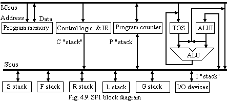 architectural
block diagram of the SF1. The SF1 has two busses. The MBUS is
multiplexed to transfer addresses to program memory and then
instructions and data to or from program memory. The SBUS is used to
transfer data between system resources. The two-bus design allows
instructions to be fetched on the MBUS while data operations are
taking place on the SBUS. The ALU has an associated top-of-stack
register (TOS) which receives the results of all ALU operations.
architectural
block diagram of the SF1. The SF1 has two busses. The MBUS is
multiplexed to transfer addresses to program memory and then
instructions and data to or from program memory. The SBUS is used to
transfer data between system resources. The two-bus design allows
instructions to be fetched on the MBUS while data operations are
taking place on the SBUS. The ALU has an associated top-of-stack
register (TOS) which receives the results of all ALU operations.
The ALU input register (ALUI) acts as a holding buffer to contain the second operand for the ALU. ALUI may be loaded from either the SBUS for most operations, or the MBUS for memory fetches. Both the ALUI and the TOS may be routed to the MBUS or the SBUS. The TOS register by convention contains the top stack element of whatever stack is being used for a particular instruction, although it is up to the programmer to ensure it is managed properly. There are eight different sources and destinations connected to the stack bus: S, F, R, L, G, C, I, and P: S - general purpose stack for parameters; L - loop counter stack; G - global stack; F - frame stack; R - return address stack; C - in-line constant value; I - I/O address space; P - Program counter. All eight are referred to as stacks in the machine's reference material, but in reality the C, I, and P resources are special non-stack structures. The stacks L, G, F, and R are for the most part interchangeable in practice, and may be used for any purpose. The S stack is somewhat specialized in that all subroutine return addresses are automatically pushed onto the S stack. The Program Counter (PC) is a counter that can be asserted on the MBUS to provide addresses for instructions as well as loaded from the MBUS for jumps and subroutine calls. The PC can also be read and written on the SBUS to save and restore subroutine return addresses.