

Questions for Self-Testing
1. How much had the speed of arithmetic operations execution in high-performance computers been increased before appearing systems-on-chip?
2. What microoperations are considered elementary?
3. What is computer arithmetic?
4. How is the addition operation performed?
5. What are the peculiarities of the subtraction operation?
2.3. Operands Multiplication Operation
Multiplication
of Positive Numbers. The
usual “paper-and-pencil” algorithm for multiplication of integers
represented in any positional number system is illustrated in Fig.
2.7,a
for the binary system, assuming positive 4-bit operands. The product
of two n-digit
numbers can be accommodated in 2n
digits, so the product in this example fits into 8 bits, as shown. In
the binary system, multiplication of the multiplicand by 1 bit of the
multiplier is easy. If the multiplier bit is 1, the multiplicand is
entered in the appropriately shifted position to be added with other
shifted multiplicands to form the product. If the multiplier
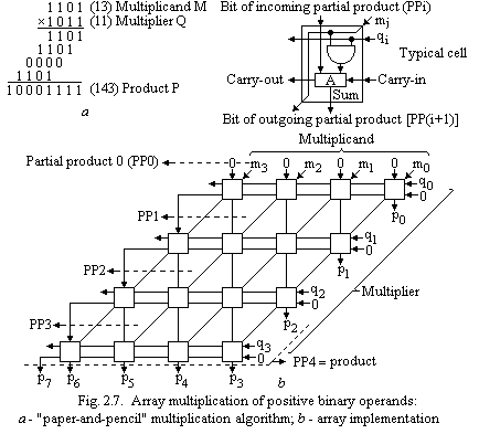 bit
is 0, then 0s are entered as in the third row of the example. It is
possible to implement positive operand binary multiplication in a
purely combinational two-dimensional logic array, as shown in Fig.
2.7,b.
The main component in each cell is an Adder circuit. The AND gate in
any cell determines whether or not a multiplicand bit mj
is added to the incoming partial-product bit, based on the value of
the multiplier bit qi.
Each row i,
0 ≤ i
≤ 3, of this array adds the multiplicand (appropriately shifted) to
the incoming partial product PPi
to generate the outgoing partial product PP(i
+ 1) if qi
= 1. If qi
= 0, PPi
is passed vertically down unchanged. PP0 is obviously all 0s, and PP4
is the desired product. The multiplicand is shifted left one position
per row by the diagonal signal path.
bit
is 0, then 0s are entered as in the third row of the example. It is
possible to implement positive operand binary multiplication in a
purely combinational two-dimensional logic array, as shown in Fig.
2.7,b.
The main component in each cell is an Adder circuit. The AND gate in
any cell determines whether or not a multiplicand bit mj
is added to the incoming partial-product bit, based on the value of
the multiplier bit qi.
Each row i,
0 ≤ i
≤ 3, of this array adds the multiplicand (appropriately shifted) to
the incoming partial product PPi
to generate the outgoing partial product PP(i
+ 1) if qi
= 1. If qi
= 0, PPi
is passed vertically down unchanged. PP0 is obviously all 0s, and PP4
is the desired product. The multiplicand is shifted left one position
per row by the diagonal signal path.
Although
the above combinational multiplier is quite easy to understand, it is
usually impractical to use in computers because it uses a large
number of gates and performs only one function. Many computers that
provide multiplication in the basic machine instruction set implement
it by a sequence of operations, as shown in Fig. 2.8. The block
diagram in part (a)
of the figure describes a suitable hardware arrangement. This circuit
performs multiplication by using the single adder n
times to implement the addition being performed spatially by the n
rows of ripple-carry adders of Fig. 2.7,b.
The combination of
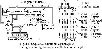 registers
A and Q holds PPi
during the time that multiplier bit qi
is generating the signal ADD/NOADD. This signal controls the addition
of the multiplicand M to PPi
to generate PP(i
+ 1). There are n
cycles needed to compute the product. The partial product grows in
length by 1 bit per cycle from the initial vector (PP0) of n
0s in register A. The carry-out from the adder is stored in flip-flop
C shown at the left end of register A. At the start, the multiplier
is loaded into register Q, the multiplicand into register M, and C
and A are set to 0. At the end of each cycle, C, A, and Q are shifted
right one bit position to allow for growth of the partial product as
the multiplier is shifted out of register Q. Because of this
shifting, multiplier bit qi
appears at the LSB position of Q to generate the ADD/NOADD signal at
the correct time, starting with q0
during the first cycle, q1
during the second, etc. After use, the multiplier bits can be
discarded. This is accomplished by the right-shift operation. Note
that the carry-out from the adder is the leftmost bit of PP(i
+ 1), and it must be held in the C flip-flop to be shifted right with
the contents of A and Q. After n
cycles, the high-order half of the product is held in register A and
the low-order half is in register Q. The multiplication example of
Fig. 2.7,a
is shown in Fig. 2.8,b
as it would be performed by the above hardware arrangement.
registers
A and Q holds PPi
during the time that multiplier bit qi
is generating the signal ADD/NOADD. This signal controls the addition
of the multiplicand M to PPi
to generate PP(i
+ 1). There are n
cycles needed to compute the product. The partial product grows in
length by 1 bit per cycle from the initial vector (PP0) of n
0s in register A. The carry-out from the adder is stored in flip-flop
C shown at the left end of register A. At the start, the multiplier
is loaded into register Q, the multiplicand into register M, and C
and A are set to 0. At the end of each cycle, C, A, and Q are shifted
right one bit position to allow for growth of the partial product as
the multiplier is shifted out of register Q. Because of this
shifting, multiplier bit qi
appears at the LSB position of Q to generate the ADD/NOADD signal at
the correct time, starting with q0
during the first cycle, q1
during the second, etc. After use, the multiplier bits can be
discarded. This is accomplished by the right-shift operation. Note
that the carry-out from the adder is the leftmost bit of PP(i
+ 1), and it must be held in the C flip-flop to be shifted right with
the contents of A and Q. After n
cycles, the high-order half of the product is held in register A and
the low-order half is in register Q. The multiplication example of
Fig. 2.7,a
is shown in Fig. 2.8,b
as it would be performed by the above hardware arrangement.
We can now relate the components of Fig. 2.8,a to Fig. 1.3. Assume that the multiply sequence is to be hardwired as a machine instruction. Furthermore, assume that the multiplier and multiplicand are in R2 and R3, respectively, and that the two-word product is to be left in R1 and R2. First, the multiplicand is moved into register Y. Thus register Y corresponds to M, and R1 and R2 correspond to A and Q in Fig. 2.8,a. Connections must be made so that R1 and R2 can be right-shifted as a two-word combination. A transfer from Z to R1 is made after each cycle. The C bit in Fig. 2.8,a is actually the carry flag in the condition codes. It must be connectable to R1 for shifting operations as in Fig. 2.8,a.
Signed-Operand Multiplication. Multiplication of signed operands generating a double-length product in the 2's-complement number system requires a few further remarks about that representation. We will not discuss multiplication in the other representations because it reduces to the multiplication of positive operands already discussed. The accumulation of partial products by adding versions of the multiplicand as selected by the multiplier bits is still the general strategy.
L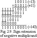 et
us first consider the case of a positive multiplier and a negative
multiplicand. When we add a negative multiplicand to a partial
product, we must extend the sign-bit value of the multiplicand to the
left as far as the extent of the eventual product. Consider the
example shown in Fig. 2.9, where the 5-bit signed operand -13
(multiplicand) is multiplied by +11 (multiplier) to get the
10-bit product -143. The sign extension of the multiplicand is shown
underlined. To see why this sign-extension operation is correct,
consider the following argument. The extension of a positive number
is obviously achieved by the addition of zeroes at the left end. For
the case of negative numbers, consider Fig. 2.4. It is easily seen by
scanning around the mod 16 circle in the counterclockwise direction
from the code for 0 that if 5-bit, 6-bit, 7-bit, etc., negative
numbers were written out, they would be derived correctly by
extending the given 4-bit codes by 1s to the left. This sign
extension must be done by any hardware or software implementation of
the multiply operation.
et
us first consider the case of a positive multiplier and a negative
multiplicand. When we add a negative multiplicand to a partial
product, we must extend the sign-bit value of the multiplicand to the
left as far as the extent of the eventual product. Consider the
example shown in Fig. 2.9, where the 5-bit signed operand -13
(multiplicand) is multiplied by +11 (multiplier) to get the
10-bit product -143. The sign extension of the multiplicand is shown
underlined. To see why this sign-extension operation is correct,
consider the following argument. The extension of a positive number
is obviously achieved by the addition of zeroes at the left end. For
the case of negative numbers, consider Fig. 2.4. It is easily seen by
scanning around the mod 16 circle in the counterclockwise direction
from the code for 0 that if 5-bit, 6-bit, 7-bit, etc., negative
numbers were written out, they would be derived correctly by
extending the given 4-bit codes by 1s to the left. This sign
extension must be done by any hardware or software implementation of
the multiply operation.
We will now consider the case of negative multipliers. A straightforward solution is to form the 2's complement of both the multiplier and the multiplicand and proceed as in the case of a positive multiplier. This is possible, of course, since complementation of both operands does not change the value or the sign of the product. Another technique that works correctly for negative numbers in the 2's-complement representation is to proceed as follows. Add shifted versions of the multiplicand, properly sign-extended, just as in the case of positive multipliers, for all 1 bits of the multiplier to the right of the sign bit. Then add -1 × multiplicand, properly shifted, as the contribution to the product determined by the 1 in the sign-bit position of the multiplier. The sign position is thus viewed as the same as the other positions, except it has a negative weight. The justification for this procedure will be discussed more fully later in this section.
A powerful direct algorithm for signed-number multiplication is the Booth algorithm. It generates a 2n-bit product and treats both positive and negative numbers uniformly. Consider a multiplication operation in which a positive multiplier has a single block of 1s with at least one 0 at each end, for example, 0011110. To derive the product, we could add four appropriately shifted versions of the multiplicand as in the standard procedure. However, the number of required operations can be reduced by observing that a multiplier in this form can be regarded as the difference of two numbers as follows:
0 1 0 0 0 0 0 (32)
- 0 0 0 0 0 1 0 (2)
0 0 1 1 1 1 0 (30)
This suggests generating the product by one addition and one subtraction operation. In particular, in the above case, adding 25 × multiplicand and subtracting 21 × multiplicand gives the desired result.
F or
convenience in later discussions, we will represent the standard
scheme by writing the multiplier as 0 0 +1 + 1 +1 +1 0, and the new
recoding scheme by writing the multiplier as 0 +1 0 0 0 -1 0. Note
that in the new scheme -1 × (shifted multiplicand) is selected at
0→1 boundaries and +1 × (shifted multiplicand) is selected at 1→0
boundaries as the multiplier is scanned from right to left. Fig. 2.10
illustrates the two schemes. This clearly extends to any number of
blocks of 1s in a multiplier including the situation where a single 1
is considered a block. See Fig. 2.11 for another example. Until now
we have shown positive multipliers. Since there is at least one 0 at
the left end of any multiplier, a +1 operation can be operation to
preserve the correctness of the operation. It is also true that if we
apply the method to a negative multiplier, we get the correct answer.
An example is given in Fig. 2.12. To show the correctness of this
technique we need to introduce a property
or
convenience in later discussions, we will represent the standard
scheme by writing the multiplier as 0 0 +1 + 1 +1 +1 0, and the new
recoding scheme by writing the multiplier as 0 +1 0 0 0 -1 0. Note
that in the new scheme -1 × (shifted multiplicand) is selected at
0→1 boundaries and +1 × (shifted multiplicand) is selected at 1→0
boundaries as the multiplier is scanned from right to left. Fig. 2.10
illustrates the two schemes. This clearly extends to any number of
blocks of 1s in a multiplier including the situation where a single 1
is considered a block. See Fig. 2.11 for another example. Until now
we have shown positive multipliers. Since there is at least one 0 at
the left end of any multiplier, a +1 operation can be operation to
preserve the correctness of the operation. It is also true that if we
apply the method to a negative multiplier, we get the correct answer.
An example is given in Fig. 2.12. To show the correctness of this
technique we need to introduce a property
|
|

|
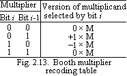
The Booth technique for recoding or reinterpreting multipliers is summarized in Fig. 2.13.
Fast Multiplication. The basic transformation 011…110 => + 100…0-10 that is fundamental to the Booth algorithm has been called the "skipping over 1s" technique. The motivation for this term is that in cases where the multiplier has its 1s grouped into a few contiguous blocks, only a few versions of the multiplicand (summands) need to be added to generate the product. If only a few summands need to be added, the multiplication operation can potentially be speeded up. However, in the worst case, that of alternating 1s and 0s in the multiplier each bit of the multiplier selects a summand. In fact, this results in more summands than if the Booth algorithm is not used. A 16-bit "worst case" multiplier, a more "normal" multiplier, and a "good" multiplier are shown in Fig. 2.14.

The Booth algorithm thus actually achieves two purposes. First, it uniformly transforms both positive and negative n-bit multipliers into a form that selects appropriate versions of n-bit multiplicands which are added to generate correctly signed 2n-bit products in the 2's-complement number representation system. Second, it achieves some efficiency in the number of summands generated when the multiplier has a few large blocks of 1s. The speed gain possible by skipping over 1s is clearly data-dependent.
We will now describe a multiplication speedup technique, which guarantees that an n-bit multiplier will generate at most n/2 summands and which uniformly handles the signed-operand case. This represents a multiplication speedup by a factor of 2 over the worst-case Booth algorithm situation.
The
new technique can be derived from the Booth technique. Recall that in
the Booth technique multiplier bit qi
selects a summand as a function of the bit qi-1
on its right. The summand selected is shifted i
binary positions to the left of the LSB position of the product
before the summand is added. Let us call this "summand position
i"
(SPi).
The basic idea of the speedup technique is that bits i
+ 1 and i
select one summand, as a function of bit i
- 1, to be added at SPi.
To be practical, this summand must be easily derivable from the
multiplicand. The n/2
summands are thus selected by bit pairs (x1,
x0),
(x3,
x2),
(x5,
x4),
etc. The technique is called the bit-pair recoding method. Consider
the multiplier of
Fig. 2.12, repeated in Fig. 2.15,a.
Grouping the Booth-recoded selectors in pairs, we obtain a single,
appropriately shifted summand for each pair as shown. The rightmost
Booth pair (-1, 0) is equivalent to -2 × (multiplicand M) at SP0.
The next pair, (-1, +1), is equivalent to -1 × M at SP2; finally,
the
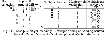 leftmost
pair of zeros is equivalent to 0 × M at SP4. Restating these
selections in terms of the original multiplier bits, we have the
cases (1, 0) with 0 on the right selects -2 × M, (1,0) with 1 on the
right selects -1 × M, and (1, 1) with 1 on the right selects 0 × M.
The complete set of eight cases is shown in
Fig. 2.15,b,
and the multiplication example of Fig. 2.12 is shown again in Fig.
2.16 as it would be computed using the bit-pair recoding method.
leftmost
pair of zeros is equivalent to 0 × M at SP4. Restating these
selections in terms of the original multiplier bits, we have the
cases (1, 0) with 0 on the right selects -2 × M, (1,0) with 1 on the
right selects -1 × M, and (1, 1) with 1 on the right selects 0 × M.
The complete set of eight cases is shown in
Fig. 2.15,b,
and the multiplication example of Fig. 2.12 is shown again in Fig.
2.16 as it would be computed using the bit-pair recoding method.

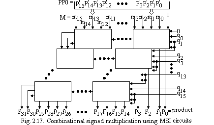
It is possible to extend the sequential hardware multiplication circuit of Fig. 2.8 to implement both the signed-operand (Booth) algorithm and the bit-pair recoding speedup technique. Instead of a sequential circuit, we will describe circuit, copies of which can be interconnected in a planar array to implement signed-number multiplication combinationally. The circuit is based on the bit-pair recoding technique and uses carry lookahead to achieve high-speed addition of a summand and a partial product. Consider the multiplication of two 16-bit signed numbers, producing a 32-bit signed product.
Fig. 2.17 shows the arrangement of 2 × 4 multiplier circuits with the input operands applied. Each row of four circuits takes the partial-product (PP) input at its row level and adds the summand determined by its multiplier pair inputs to generate the PP output for the next row. Since eight rows are needed in the case shown, a 16 × 16 multiplication can be implemented with thirty-two 2 × 4 circuits. The name 2 × 4 is derived from the fact that each circuit inspects 2 bits of the multiplier and operates on a 4-bit slice of the partial product.
T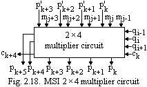 here
are a number of details that have not been covered in the above
overall description. Fig. 2.18 shows a 2 × 4 circuit with its inputs
and outputs labeled to indicate that its position is in the row
corresponding to multiplier bits qi
and qi+1.
One of its input vectors from the top is the 4-bit slice p'k+3,
p'k+2,
p'k+1,
p'k
of the incoming partial product. The other input vector from the top
is the 4-bit slice mj+3,
mj+2,
mj+1,
mj
of the appropriately shifted multiplicand. A fifth bit, mj-1,
from the multiplicand is also provided. This bit is needed if ±2 ×
M is to be applied at this row level. This chip generates the 4-bit
slice pk+3,
pk+2,
pk+1,
pk
of the outgoing partial product. Although carries are determined
internally in each 2 × 4 circuit by carry lookahead techniques, the
carries ck,
ck+4,
etc., ripple laterally between circuits in performing the required
addition. Finally, since signed numbers are being handled, the
left-end 2 × 4 circuit of any row must implement a partial-product
extension operation (with correct sign extension). This is necessary
to provide the left pair of partial-product inputs to the 2 × 4
circuit directly below it in the next row. In Fig. 2.18, output bits
Pk+5
and Pk+4
are the extension bits. These outputs are used only in the 2 × 4
circuits at the left end of each row. In the last row, they
constitute bits p31
and p30
of the 32-bit product in the example of Fig. 2.17.
here
are a number of details that have not been covered in the above
overall description. Fig. 2.18 shows a 2 × 4 circuit with its inputs
and outputs labeled to indicate that its position is in the row
corresponding to multiplier bits qi
and qi+1.
One of its input vectors from the top is the 4-bit slice p'k+3,
p'k+2,
p'k+1,
p'k
of the incoming partial product. The other input vector from the top
is the 4-bit slice mj+3,
mj+2,
mj+1,
mj
of the appropriately shifted multiplicand. A fifth bit, mj-1,
from the multiplicand is also provided. This bit is needed if ±2 ×
M is to be applied at this row level. This chip generates the 4-bit
slice pk+3,
pk+2,
pk+1,
pk
of the outgoing partial product. Although carries are determined
internally in each 2 × 4 circuit by carry lookahead techniques, the
carries ck,
ck+4,
etc., ripple laterally between circuits in performing the required
addition. Finally, since signed numbers are being handled, the
left-end 2 × 4 circuit of any row must implement a partial-product
extension operation (with correct sign extension). This is necessary
to provide the left pair of partial-product inputs to the 2 × 4
circuit directly below it in the next row. In Fig. 2.18, output bits
Pk+5
and Pk+4
are the extension bits. These outputs are used only in the 2 × 4
circuits at the left end of each row. In the last row, they
constitute bits p31
and p30
of the 32-bit product in the example of Fig. 2.17.
F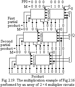 ig.
2.19 shows the input and output variables of each of six 2 × 4
multiplier circuits of an array implementation of the multiplication
example shown on the right side of Fig. 2.16. Note that although the
example is a 5 × 5 multiplication, this array can handle up to an 8
× 6 case. The first partial product in Fig. 2.19 corresponds to the
first summand on the right side of Fig. 2.16. It can easily be
checked that the second partial product is the sum of the first and
second summands. Since the third summand is 0, this second partial
product is the final answer (the product).
ig.
2.19 shows the input and output variables of each of six 2 × 4
multiplier circuits of an array implementation of the multiplication
example shown on the right side of Fig. 2.16. Note that although the
example is a 5 × 5 multiplication, this array can handle up to an 8
× 6 case. The first partial product in Fig. 2.19 corresponds to the
first summand on the right side of Fig. 2.16. It can easily be
checked that the second partial product is the sum of the first and
second summands. Since the third summand is 0, this second partial
product is the final answer (the product).
Although this discussion has been rather sketchy, it is intended to give the reader some grasp of the algorithms that have been used in commercially available MSI circuits that are intended for high-performance signed-integer multiplication. These and similar circuits can be used in both general-purpose computers and special-purpose digital processors where arithmetic operation speeds are critical.
High-Speed Multiplier Design. Previously reported algorithms mainly focused on rapidly reducing the partial products rows down to final sums and carries used for the final accumulation. These techniques mostly rely on circuit optimization and minimization of the critical paths. Rather than focusing on reducing the partial products rows down to final sums and carries, it is possible to generate fewer partial products rows. In turn, this influences the speed of the multiplication, even before applying partial products reduction techniques. Fewer partial products rows are produced, thereby lowering the overall operation time.
There are three major steps to any multiplication. In the first step, the partial products are generated. In the second step, the partial products are reduced to one row of final sums and one row of carries. In the third step, the final sums and carries are added to generate the result. Most of the above-mentioned approaches employ the Modified Booth Encoding (MBE) approach [16, 18] for the first step because of its ability to cut the number of partial products rows in half. They then select some variation of any one of the partial products reduction schemes, such as Wallace trees or compressor trees, in the second step to rapidly reduce the number of partial product rows to the final two (sums and carries). In the third step, they use some kind of advanced adder approach such as carry-lookahead or carry-select adders, to add the final two rows, resulting in the final product.
The main focus of recent multiplier papers has been on rapidly reducing the partial product rows by using some kind of circuit optimization and identifying the critical paths and signal races. In other words, the goals have been to optimize the second step of the multiplication.
It is possible to concentrate on the first step, which consists of forming the partial product array and to design a multiplication algorithm which will produce fewer partial product rows. By having fewer partial product rows, the reduction tree can be smaller in size and faster in speed. The multiplier architecture to generate the partial products is shown in Fig. 2.20.
The only difference between this architecture and the conventional multiplier architectures is that, for the last partial product row, this architecture has no partial product generation but partial product selection with a two's complement unit. The 3-5 coder selects the correct value from five possible inputs (2 × X, 1 × X, 0, -1 × X, -2 × X) which are either coming from the two's complement logic or the multiplicand itself and input into the row of 5-1 selectors. Unlike the other rows which use PPRG (Partial Product Row Generator), the two's complement logic does not have to wait for MBE to finish: The two's complementation is performed in parallel with MBE and the 3-5 decoder.
Hardware multipliers and dividers had been used to increase the speed of arithmetic operations in high-performance computers before appearing systems-on-chip. With appearing such systems, the return to old methods of multiplication operation performing without using the method of increasing has been become. That’s why, at the given stage of the computer engineering evolution, only methods of the matrix multiplication accelerators are widely used for multimedia applications.
