

6 Laboratory tasks.
Content of the work
6.1 To study the theoretical material about the features of schematic implementation of a bridge circuit of rectification, processes of operation, areas of application by the recommended literature. To study the principle scheme of the stand and features of its functioning.
6.2 To calculate the electrical parameters of the scheme working on the load with capacitive response.
6.3 Calculate the electrical parameters of the scheme working on the load with an inductive response.
6.4 Investigate the scheme of single-phase bridge rectifier for different types k of load of the rectification block RF : on active load (k = 1); on inductive load (k = 2); on capacitive load (k = 3); on Г-type LC-filter (k = 4); in П-type CLC-filter (k = 5).
6.4.1 Investigate external (load) characteristics of the rectifier
6.4.2 Determine the output resistance of the rectifier.
6.4.3 Determine the percentage reduction of output voltage rectifier.
6.4.4 Investigate filtering properties of rectifying filters of the rectifier: Kпв, Kпн, KпвU, KпнU, Si, SU = f (Iн).
6.4.5 Investigate the processes of the functioning of the rectifier.
6.5 To make the conclusions on the results of the performed work.
7 Methods of laboratory work processing
7.1 To the point 6.1. Program and order to the study of theoretical issues.
To study the purpose, peculiarities of structural, functional, schemo-technical constructing of rectifying devices and processes of their operation based on this laboratory work and recommended literature [2.1 ... 2.5]. To study the features of schemo-technical implementation and operation of the laboratory stand (see point 3). Get test questions by the studied material and prepare answers to them. Check with the teacher form and volume of their presentation in the report. NOTE. Stop further execution of laboratory work without the permission of the teacher. An obligatory condition for permission to perform work is an understanding of features of schemo-technical performance of the laboratory stand (see point3). 7.2 To the point 6.2 Calculation of electrical parameters of the rectification circuit with its work load with capacitive response
Calculation of a bridge circuit goes to analytic determination of the values of voltage and current of elements of rectifier’s scheme.
Initial data:
1) constant component of the rectified current І0 = Iн = 0,5... 5 А and the constant component of the rectified voltage U0 = ±Uн = 20...30 В (given by teacher);
2) transformation coefficient n12 = 5…15 of transformer Т1;
3) frequency of the feeding net fc = 50…400 Hz;
4) Effective voltage of feeding net Uс = UG1 = 198… 242 В.
As a result of calculation we determined the following:
1) Satisfying the condition of the rectification circuit work on the load with capacitive response, ie,.
Сн >> 1/4π fcmRн, Сн >> 10/4π fcmRн;
2) A main calculated coefficient A, which connects a cut-off angle of the valve with the parameters of the rectification circuit, in the form
А = tgθ – θ = πrФ / mRн,
where rФ –active resistance of the phase of rectification scheme, in this case rФ = 120 Оhm; m = 2 – phase character of the rectification circuit;
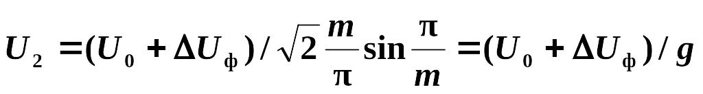
3) effective voltage U2 of secondary winding W2 of transformer TV1 – (pic. 3.3):
![]() ,
,
where
B
= f (A)
is defined by В
= 0,75 + 1,2А
while
А
![]() 0,5
or by the graph [2.4,
p.130; 2.2,
p.118];
0,5
or by the graph [2.4,
p.130; 2.2,
p.118];
4) average value of the current of the phase of the rectification circuit
Icp = I0/m;
5) effective (rms) value of the current valve
IB = DIср,
whеre D = f (A) is defined as D =2 + 1/27 А while А 0,5 or by the graph [2.4, p.130; 2.2, p.119];
6) effective value of current I2 of secondary winding of the transformer
![]() .
.
7) maximum (peak) value of current of the diode and the secondary winding of the transformer:
I2m = FIcp,
wherе F = f (A) is defined as F = 5 + 0,25 А while А 0,5 or by the graph [2.4, p.132; 2.2, p.119];
8) effective value of current Iс = IG1, consumed from the power source and the current I1 of primary winding of the transformer
IG1 = I1 = Iс = n21 I2 = I2 /n12;
9) peak reverse voltage appearing across valve
Uобр
m
=
0,5(I+B![]() )U0;
)U0;
10) coefficient of valve usage by the kU and current ki:
kU = Uобр /U0; ki = I2m / IB;
11) coefficient of the scheme
kcx = U0 / U2;
12) coefficient of transformer usage by power
Kтр
=
P0/Sтр
=
2K1K2/(K1+K2)
=![]() /BD,
/BD,
wherе K1 = P0/S1, K2 = P0/S2 – coefficient of usage of primary and secondary windings of transformer correspondingly;
S1 = IсUс, S2 = I2U2, Sтр = 0,5(S1 + S2) – total (overall) power of the primary, secondary windings and the transformer, respectively, ВА;
P0 = U0 I0 = Uн Iн – полезная мощность на выходе выпрямителя, W.
Fill out the following calculation of the relevant part of the table 7.1.
The results of calculation to reflect in the table 7.1.
7.3. to point 6.3Calculation of electrical parameters of the rectification circuit while it is working under load with an inductive response.
The calculation scheme is carried out on the following initial data:
the constant component of the rectified current I0 = 0,5...5 А (given by teacher);
Table 7.1 – Results of the research
Values of loads |
I0, А |
U0, В |
Icр, А |
IB, А |
I2m, А |
Iс, А |
Uс, В |
U2, В |
I2, А |
A |
B |
D |
F |
θ |
kU |
ki |
Kсх |
Kтр |
Capacitive load |
Calc. |
|
|
|
|
|
|
220 |
|
|
|
|
|
|
|
|
|
|
Exp. |
|
|
|
|
|
|
220 |
|
|
|
|
|
|
|
|
|
|
|
Inductive load |
Calc. |
|
|
- |
- |
- |
- |
220 |
|
|
|
|
|
|
|
|
|
|
Exp. |
|
|
- |
- |
- |
- |
220 |
|
|
|
|
|
|
|
|
|
|
the constant component of the rectified voltage U0 = 20...30 В (given by teacher);
transformation coefficient of the transformer n12 = 5…15;
active resistance of the inductance L of the filter is RФ= … Ом; frequency of feeding net fс = 50…400 Hz,
voltage Uс = 198…242 В.
As a result of calculation we determined the following:
1) voltage U2 of secondary winding of the transformer:
 ,
,
where
![]() –
drop
of the constant component of the rectified voltage on the active
resistance of the inductance of L filter;
g
–
coefficient
of rectifying scheme;
–
drop
of the constant component of the rectified voltage on the active
resistance of the inductance of L filter;
g
–
coefficient
of rectifying scheme;
2) voltage U1 of primary winding of the transformer
U1 = Uc = UG1 = U2 / n21 = U2n12 ;
3) effective value of the current through the valve
IB
= I0
/![]() ;
;
4) effective value of the current I2 of secondary winding of the transformer
I2 = IB;
5)
effective value of the current а
I1
of
primary winding of the transformer,
current
consumed from the networkI1
=
Iс
=
IG1
=
n21![]() ;
;
6)
maximum
reverse voltage across valve![]() ;
;
7) coefficient of usage of the valve by voltage kU and current ki:
kU = π / 2; ki = 0,707;
8) coefficients of scheme
kсх = U0 / U2;
9) coefficient of usage of the transformer by power:
![]() /S1;
/S1;
![]() /S2;
/S2;
![]() /S
/S![]() ,
,
where
![]() .
.
Results put to the table 7.1.
7.4 To the Paragraph 6.4. Investigation of the work of the bridge rectifier for different types k of load of rectification block RB: on active load(k = 1); on inductive load (k = 2); on capacitive load (k = 3); on Г-type LC-filter (k = 4); on П-type CLC-filter (k = 5).
Providing of needed variant k of the load of rectification block RB of the bridge rectifier is done by the switch of researched circuit selection (see pic. 3.1).
To ensure the required parameters of the circuit elements and modes of work of rectifier circuits can be used Shortcuts (keys for fast access)“G1”, “TV1”, “L1”, “C1”, “C2”, “ Rн”, “SW1” (see pic. 3.1).
7.4.1 To the Paragraph 6.4.1 Research of external (load) characteristics of the rectifier.
external characteristics – is a dependence of the voltage Uн in the load of the rectifier on current Iн through the load Uн = f (Iн).
Methods of external characteristics studying involves the following steps: choose by selection switch the needed researched circuit (see pic. 3.1) – “Active load” (k = 1– see pic. 3.2), “Inductive load”(k = 2 – рiс. 3.3);
to control the source’s parameters G1 (voltage UG1 = UG1 ном, needed frequency fс), using the key “G1” on the instrument panel (see pic. 3.1) for appearance of editing window;
to control the transformer’s parameters ТV1 – the transformation coefficient of the transformer n12 (see pic. 3.1 – key “ТV1”);
correct the element’s parameters L1, C1, C2 of rectifying filter of the rectifier, using the keys(see pic. 3.1) “L1”, “С1”, “C2”, set them to nominal value L1ном, С1ном, C2ном;
using the switch SW1, switch off the load Rн of two-semi-cycle circuit of rectification;
begin modeling, pressing “Start”;
measure by voltmeter PV3 the output voltage Uн хх in the non-conductive mode, results put into the table 7.2 (k);
switch the load on Rн;
changing resistance Rн of the load from maximum (minimum) to minimum (maximum), to measure the output voltage Uн and current Iн of the load Rн. Measured parameters put into the table 7.2 (k).
Using the results of researches build the characteristics.
Таble 7.2 (k) – Results of researches
Rн, Оhm |
¥ |
100 |
50 |
25 |
15 |
10 |
5 |
3 |
1 |
Uн, V |
|
|
|
|
|
|
|
|
|
Iн, А |
|
|
|
|
|
|
|
|
|
ΔUн, V |
|
|
|
|
|
|
|
|
|
ΔIн, А |
|
|
|
|
|
|
|
|
|
rв, Оhm |
|
|
|
|
|
|
|
|
|
7.4.2To the paragraph 6.4.2. Determination of the rectifier output resistance.
Output resistances rв of the rectifier are defined using the table of measurements. 7.4.1 (see таble 7.2 (k)):
rв = ∆Uн /∆Iн;
∆Uн = Uн max – Uн; ∆Iн = Iн max – Iн,
wherе Uн max , Iн max – maximum values of voltage and current of the load (see table. 7.2 (k)).
Results of calculations ΔUн, ΔIн, rв put into the table 7.2 (k).
7.4.3 2To the paragraph 6.4.3. Determination of percentage decreases of the output voltage of rectifier.
Percentage decreases ∆Uн% of the output voltage of rectifier while switching from non-conducting mode with voltage Uн хх to nominal load with output voltage Uн ном is defined using the results of paragraph 7.4.1 (see table. 7.2 (k)):
 .
.
7.4.4 To paragraph 6.4.4. Investigation of filtering properties of rectifying filters of the bridge rectifier.
For measurement of parameters of variables components at the output of rectification block RB, frequency fв и and width ∆Uв~ of voltageв(t) and width ∆Iв~ of current iв(t) it is necessary to connect (see pic. В.13 paragraph В.1) oscilloscope to control points: in the first case to “P0,U” – voltage uв(t) on the output of rectification block (see table. 3.3), in the second case to “P0, I” (current iв(t) on the output of rectification block – see table. 3.3).
For measurement of parameters of variables components in the load of rectifier of frequency fн u and with ∆Uн~ of voltage uн(t) and width ∆Iн~ of current iн(t) it is necessary to connect (see pic. В.13 paragraph В.1) oscilloscope to control points: in the first case to “Rн, U” – voltage uн(t) of the load Rн of rectifier (see table 3.3), in the second case to “Rн, I” – current iн(t) in the load Rн of rectifier.
Experimental values of frequencies fв и and fн и of investigated processes are defined by oscillograms uв(t) and uн(t).
For
this
you
need
to
measure
by
a
mask
of oscilloscope
the period
duration
Т
of
observed
curve using
the values n
of multiplier
"Time/Division".
Measured
time interval Т
is defined by two values
Т
=
n![]() :
lengths
:
lengths
![]() of measured time interval on the screen of the oscilloscope
horizontally in DEVISIONS
and the value
n
of time for a division in switch "Time/Division".
of measured time interval on the screen of the oscilloscope
horizontally in DEVISIONS
and the value
n
of time for a division in switch "Time/Division".
In the given case
![]() .
.
Measuring
parameters of variable component (fв
u,
![]() Uв~,
Iв~,
fн
и,
Uн~,
Iн~)
oscilloscope is used in the mode of
close input (the switch of constant component SS is switched off–
pic. В.13
paragraph.
В.1)
of amplifier of vertical
amplification .
Uв~,
Iв~,
fн
и,
Uн~,
Iн~)
oscilloscope is used in the mode of
close input (the switch of constant component SS is switched off–
pic. В.13
paragraph.
В.1)
of amplifier of vertical
amplification .
Method of research of filtering properties of rectifying filters involves the following steps (the results of measurements recorded in the table 7.3 (k)):
using the switch of circuit selection, chose(see pic. 3.1) the needed circuit of rectifier– “Active load” (k = 1– рiс. 3.2), “Inductive load” (k = 2 – рiс. 3.3), …;
correct the transformer’s parameters ТV1 – transformation coefficient n12 of the transformer n12 = n12 ном (See рiс. 3.1 – key “ТV1”);
correct the parameters of the source G1 (voltage UG1 = UG1 ном, needed frequency fс = fс ном), using the key “G1” on the elements panel (see. рiс. 3.1) window of editing;
correct the element’s parameters L1, C1, C2 of rectifying filter of the rectifier, using the key “L1”, “C1”, “C2” on the elements panel (see. piс. 3.1), to set the nominal value L1ном, С1ном, C2ном;
begin modeling, pressing “Start” – рiс. 3.1;
set the resistance Rн = Rном of the load of rectifier, using slider “Rн” (see pic. 3.1), providing the value of current Iн = Iн ном;
measure the resistance Rн, of voltmeter PV3 and ampermeter PА3. Results Rн, Uн and Iн ном put into the table 7.3 (k);
measure the width Uв~ and frequency fв и of voltage pulsation on the output of rectification block RB using the voltage oscillograms uв(t) (control point Р0, U from the table 3.3);
measure the width
 Iв~
of current pulsation on the output of rectification block RB
using the current oscillograms iв(t)
(Р0,
I);
Iв~
of current pulsation on the output of rectification block RB
using the current oscillograms iв(t)
(Р0,
I);measure the width Uн~ and frequency fн и of voltage pulsation in the load of rectifier using the voltage oscillograms uн(t) (control point Rн, U from the table 3.3);
change the width Iн~ of current pulsation in the load of rectifier using the oscillogram iн(t) (Rн, I – таble 3.3);
to make the same measurements for currents Iн through the load, 0,75Iн ном, 0,5Iн ном and 0,25Iн ном, using slider “Rн” – see pic.. 3.1 (results put to the table. 7.3 (k));
Research on this method to perform for two versions of the rectifier load: the active and inductive loads;
Make these researches for all types k of loads of rectification block (k = 1, 2,…, 5);
perform similar measurements at different values of capacity С1 for k = 3, 4, 5 – results of measurements recorded in the table 7.4 (k);
perform similar measurements at different values of inductance of throttle L1 k = 2, 4, 5 – results put into table7.3 (k);
using the results of the experiment (table 7.3 (k), 7.4 (k), 7.5 (k)), calculate and fill the tables 7.3 (k), 7.4 (k), 7.5 (k).
Таble 7.3 (k) – Results of researches
№ |
Experimental data |
Calculated data |
||||||||||||||
Iн, А |
Uн, V |
fвu, Hz |
∆Uв~, V |
∆Iв~, А |
fнu, Hz |
∆Uн~, V |
∆Iн~, А |
|
|
Kпв |
KпвU |
Kпн |
KпнU |
Si |
SU |
|
1 2 … |
|
|
|
|
|
|
|
|
|
|
|
|
|
|
|
|
Results of experiment let us to define normalized frequencies:
![]()
![]()
The coefficients of pulsation on the output of the rectification block RB (current Kпв and voltage KпвU), in the load circuit (current Kпн and voltage KпнU ) of the rectifier:
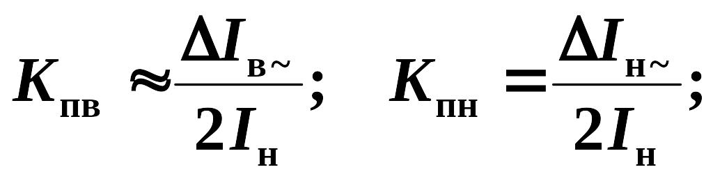

Coefficients of rectification by current Si and voltage SU are defined using the coefficients of pulsation:
![]()
Results
of calculations
![]() ,
Kпв,
Kпн,
KпвU,
KпнU,
Si,
SU
put inti
the table 7.3
(k),
7.4
(k),
7.5
(k).
,
Kпв,
Kпн,
KпвU,
KпнU,
Si,
SU
put inti
the table 7.3
(k),
7.4
(k),
7.5
(k).
Using the results build the working characteristics KпвU, KпнU, Si, SU = f (Iн, С1, L1).
7.4.5 To paragraph 6.4.5. Investigation of operation of the rectifier.
Switch (see pic. 3.1) the needed rectifier’s circuit – “Active load” (k = 1– рiс. 3.2), “Inductive load” (k = 2 – рiс. 3.3),
Set, using slider “Rн” – рiс. 3.1) load resistances Rн, current Iн, equal to the nominal value Iн =Iн ном. Draw the oscolograms of voltage u1(t) of primary transformer winding ТV1, current i1(t) of primary transformer winding ТV1, currents iVD1(t), iVD2(t), iVD3(t), iVD4(t) of diodsVD1, VD2, VD3, VD4, output current iв(t) of voltage rectifier uн(t) on the load Rн etc. (according to table. 3.3). Drawing oscillograms use equal scale by time axes, the coordinates beginnings should be on one vertical line.
Таble 7.4(k) – Results of researches
№ |
Experimental data |
Calculated data |
|||||||||||||||
C1, мкФ |
Iн, A |
Uн, V |
fвu, Hz |
∆Uв~,,V |
∆Iв~, А |
fнu, Hz |
∆Uн~, V |
∆Iн~, А |
|
|
Kпв |
KпвU |
Kпн |
KпнU |
Si |
SU |
|
1 2 … |
|
|
|
|
|
|
|
|
|
|
|
|
|
|
|
|
|
Таble 7.5 (k) – Results of researches
№ |
Experimental data |
Calculated data |
|||||||||||||||
L1, мГн |
Iн, A |
Uн, V |
fвu, Hz |
∆Uв~, V |
∆Iв~, А |
fнu, Hz |
∆Uн~V |
∆I~, А |
|
|
Kпв |
KпвU |
Kпн |
KпнU |
Si |
SU |
|
1 2 … |
|
|
|
|
|
|
|
|
|
|
|
|
|
|
|
|
|
Save the amplitude and time correlations, drawings the oscillograms, as this is essential for the analysis. Duration of the oscilloscope division is selected such that at the working part of the screen was placed 1,5 ... 2 periods of the observed waveforms. Under each image of oscillogram should indicate to what physical quantity it belongs.
Cutoff angle of current θ in the capacitive load is defined in calculated data by the relations A = tgθ–θ, and in experimental part – using current oscillogram iв(t) at the output of rectification block. Using the oscillograme find the value Т – period of pulses of current in line units of oscilloscope screen– and value tи – pulse duration of current – in same line units. After define the value θ, using the formula
θ = 360 tu/2T, эл. град.
To find А experimentally, we should use radian units of θ. (θ = 360 tu/2T, эл. град.)
Parameters B, D, F are defined by explanations to paragraph. 6.2 using the obtained value of А. Values Iв (effective value of current of valve), I2m (maximum value of the current of valve), Kтр (coefficients of transformer’s usage by power) is calculated using the experimental data, using relations from paragraph 7.2 (or7.3).
Comparison of calculation and experiment is carried out by comparing the values measured or taken experimentally. The results of measurements and calculations are summarized in table
7.1 (while Iн ном = I0 and Uн ном = U0).
7.5 To paragraph 6.5. Conclusions on the work.
Design report with regard to the requirements of section 6 of this methodological development. 6.4, plot in one coordinate system, the external characteristics of the rectifier Uн = f (Iн).
Conclusions of done work should contain a shirt and clear points, which reveal the essence of the phenomena, observed or received graphic dependencies. Conclusions should not state the external signs, but to explain to them, establishing the unity of theory and experiment, explaining the fundamental difference between one case from another (eg, the difference in the form of current flow through the valve at the different character of the load, nonlinearity, or conversely, the linearity of the external characteristics and so on .). The conclusions should show comprehension of the results of laboratory studies. Between the answers to test questions and the conclusions of the work is a direct link. Conclusions should not repeat the content of the work (section 6).