
- •Laboratory work № 1.1 Research of working modes of rectifying device (of single-phase bridge scheme of rectification and smoothing filters)
- •1 Purpose of the work
- •2 Литература
- •3 Description of laboratory stand
- •4 Home tasks
- •5 Control questions
- •6 Laboratory tasks.
- •7 Methods of laboratory work processing
- •8 Containance of the report
Laboratory work № 1.1 Research of working modes of rectifying device (of single-phase bridge scheme of rectification and smoothing filters)
1 Purpose of the work
Learning of principles of structure, functional and schemo-technical building and functioning of rectifying devices, research of their main characteristics and peculiarities of their work.
Experimental verification of calculated results of basic electro-technical values and indicators of single-phase bridge rectifier.
Experimental research of filtering properties of smoothing filters of rectifiers
Studying of methodic of experimental defining of basic characteristics of bridge rectifier, working on different types of loads
2 Литература
2.1 Электропитание устройств связи: Учебник для вузов / А.А. Бокуняев, В.М. Бушуев, А.С. Жерненко, А.Ф. Кадацкий и др.; Под ред. Ю.Д. Козляева. – М.: Радио и связь, 1998. – C. 69 – 129.
2.2 Электропитание устройств связи: Учебник для вузов / А.А.Бокуняев и др.; Под ред. В.Е.Китаева – М.: Радио и связь, 1988. – С. 87–137.
2.3 Электропитание устройств связи: Учебник для вузов / О.А. Доморацкий и др.; – М.: Радио и связь, 1981. – С. 79–138.
2.4 Китаев В.Е. и др.; Электропитание устройств связи: – М.: Связь, 1975. – С. 129–160.
2.5 Иванов-Цыганов А.И. Электропреобразовательные устройства РЭС: Учебник для вузов. – М.: Высшая школа, 1991.– С. 65–143.
.
3 Description of laboratory stand
Given laboratory stand (pic. 3.1) is aimed for researching of the bridge scheme of rectifier(Grec`s scheme) on 5 different types of loads on the rectifying block: on active load – k = 1; on inductive load – k = 2; on capacity load – k = 3; on Г-type LC-filter k = 4; на П-type CLC-filter – k = 5. Short description of researched schemes is placed in the table 3.1.
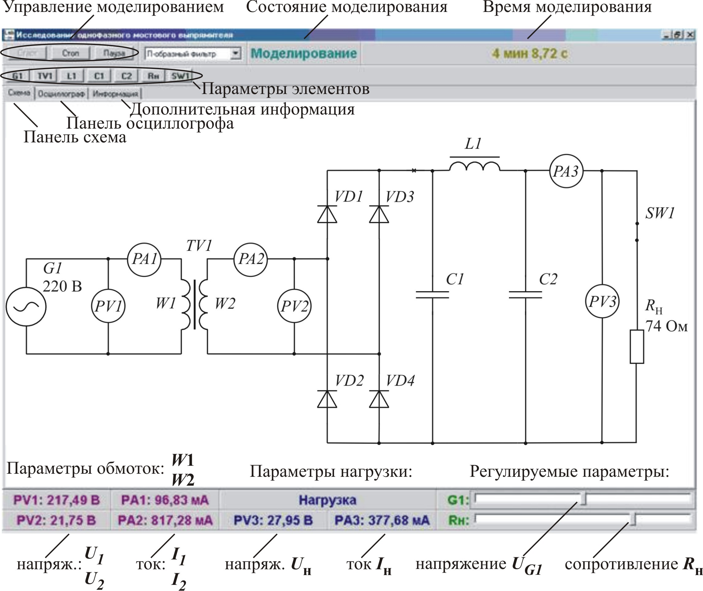
Picture 3.1 – Laboratory stand
Laboratory stand contains:
Source of sinusoidal voltage G1;
transformer ТV1;
rectifying block RF – block of semiconductor diodes VD1…VD4;
rectifying filter – elements C1, C2, L1;
regulated resistance RL of the load circle;
Table 3.1 – Description of researched schemes |
|||
k |
Designation in stand |
Description |
№ pic. |
1 |
Active load |
Scheme of rectifier with out rectifying filter– with active load. Elements L1, C1 and C2 are not used. |
3.2 |
2 |
Inductive filter |
Scheme of rectifier with active-inductive load. Elements C1 and C2 are not used. |
3.3 |
3 |
Capacity filter |
Scheme of rectifier with active-capacitive load. Elements L1 and C2 are not used |
3.4 |
4 |
Г-type filter |
Rectifier’s work with Г-type LC filter. Capacitor C2 is not used. |
3.5 |
5 |
П-type filter |
Rectifier`s work with П -type LC filter. |
3.6 |
switch SW1 of the resistance RL of the load circle;
four-beam oscilloscope – “Осциллограф”;
voltmeter PV1 of the voltage U1 of primary transformers winding ТV1;
amperemeter PA1 of the current I1 of primary transformer’s winding ТV1;
voltmeter PV2 of the voltage U2 of secondary transformer’s winding ТV1;
amperemeter PA2 of the current I2 of secondary transformer’s winding ТV1;
voltmeter PV3 of output voltage – voltage U0 of the load circle RL;
amperemeter PA3 of the current I0 of the load RL.
Laboratory stand consists of primary electro-feeding source G1; transformer ТV1, providing matching of voltage of primary electro-feeding with needed voltage of the load; rectifying block RF (VD1…VD4); rectifying filter L1, C1, C2 (depending on researched scheme) and resistance of the load RL, which can be switched off by the switch SW1. The list of elements of laboratory stand is represented in the table 3.2.The output voltage of the generator G1 and the resistance of the resister’s load RL are put on the panel of operative regulations.
Таble 3.2 – Contant of laboratory stand
Pos. |
Type of element |
Regulated parameters |
Comment |
|||
The parameter |
min. |
max. |
Unit of measurement |
|||
G1 |
Generator of sinusoidal voltage |
Output voltage |
198 |
242 |
V |
Effective value, operative regulation |
frequency |
50 |
400 |
Гц |
|
||
TV1 |
Transformer |
Transformation coefficient |
5 |
15 |
|
|
VD1 |
Diode |
|
|
|
|
|
VD2 |
Diode |
|
|
|
|
|
VD3 |
Diode |
|
|
|
|
|
VD4 |
Diode |
|
|
|
|
|
L1 |
Throttle (Дроссель) |
Inductance |
0,01 |
10 |
Гн |
Only for pictures 2, 4, 5 |
C1 |
Capacitor |
Capacitance |
50 |
104 |
мкФ |
Only for pictures 3, 4, 5 |
C2 |
Capacitor |
Capacitance |
50 |
104 |
мкФ |
Only for picture 5
|
Rн |
Resister |
Resistance |
1 |
100 |
Оhm |
Operative regulation |
SW1 |
Switch |
State |
off |
on |
|
Switch of the load |
PV1 |
Voltmeter |
|
|
|
|
Effective value |
PV2 |
Voltmeter |
|
|
|
|
Effective value |
PA1 |
Amperemeter |
|
|
|
|
Effective value |
PA2 |
Amperemeter |
|
|
|
|
Effective value |
PV3 |
Voltmeter |
|
|
|
|
Average value |
PA3 |
Amperemeter |
|
|
|
|
Average value |
P0 |
Control point |
|
|
|
|
|
Effective value of the voltage U1 and current I1 of primary transformer’s winding ТV1 is controlled by the voltmeter PV1 and ampermeter PА1. Effective value of the voltage U2 and current I2 of secondary transformer’s winding ТV1 is controlled by the voltmeter PV2 and ampermeter PА2. Average value of the voltage Uн = U0 and current Iн = I0 of the load RL are measured by the voltmeter PV3 and ampermeter PA3.
Four-beam oscilloscope, providing observation of the voltage and currents in the different points of the scheme, is included to the set of control-measuring devices. Synchronization of the oscilloscope is made automatically according to the work pf the generator G1,that is why the duration of the involute(развертки)is divided into the parts of the period of the given generator and is 0,1…100 periods/screen. List of control points of the oscilloscope is given in the table 3.3. Internal memory of the oscilloscope is enough for saving of the last period of simulation.
Table 3.3 – Researched parameters
Notation |
Oscillograms of electrical processes |
ТV1, U1 |
Voltage u1(t) of primary transformer’s winding ТV1 |
TV1, I1 |
Current i1(t) of primary transformer’s winding ТV1 |
TV1, U2 |
Voltage u2(t of secondary transformer’s winding ТV1 |
TV1, I2 |
Current i2(t) of secondary transformer’s winding ТV1 |
VD1, U |
Voltage uVD1(t) on the diode VD1 |
VD1, I |
Current iVD1(t) of the diode VD1 |
VD2, U |
Voltage uVD2(t) on the diode VD2 |
VD2, I |
Current iVD2(t) of the diode VD2 |
VD3, U |
Voltage uVD3(t) on the diode VD3 |
VD3, I |
Current iVD3(t) of the diode VD3 |
VD4, U |
Voltage uVD4(t) on the diode VD4 |
VD4, I |
Current iVD4(t) of the diode VD4 |
Rн, U |
Voltage uн(t) on the load RL |
Rн, I |
Current iн(t) of the load RL |
Р0 U |
Voltage uВ(t) on the output of rectifying block |
Р0 I |
Output current iВ(t) of rectifying block |
C1, U |
Voltage uС1(t) on the capacitor С1 |
C1, I |
Current iС1(t) of the capacitor С1 |
C2, U |
Voltage uС2(t) on the capacitor С2 |
C2, I |
Current iС2(t) of the capacitor С2 |
L1, U |
Voltage uL1(t) on the throttle L1 |
L1, I |
Current iL1(t) of the throttle L1 |
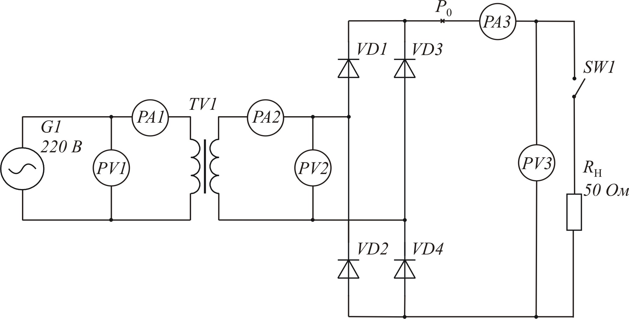
Picture 3.2 – Scheme of rectification with active load (k = 1)
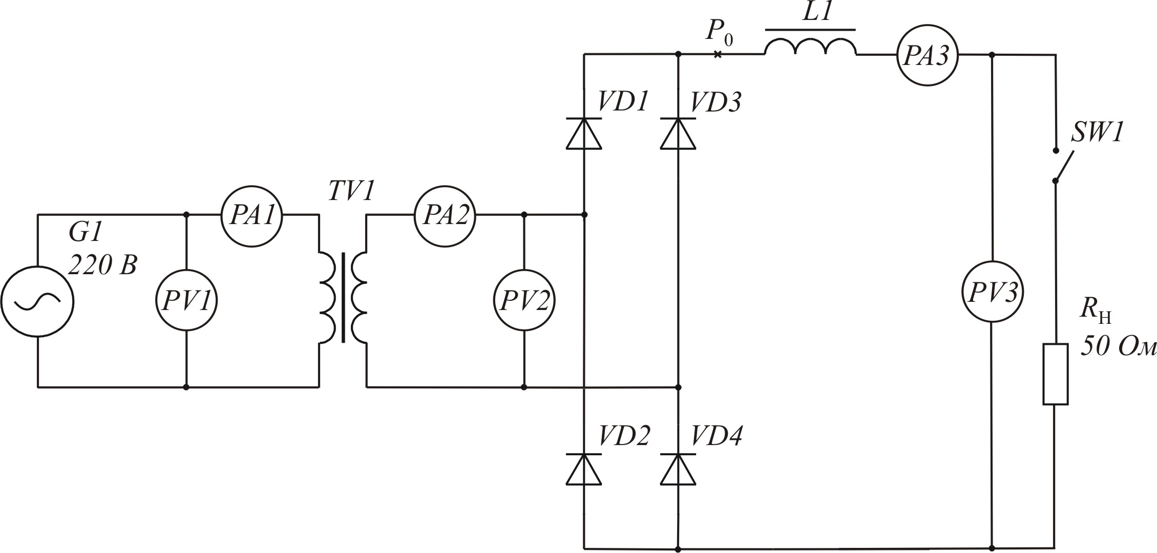
Picture 3.3 – Scheme of rectification with inductive character of the load (k = 2)
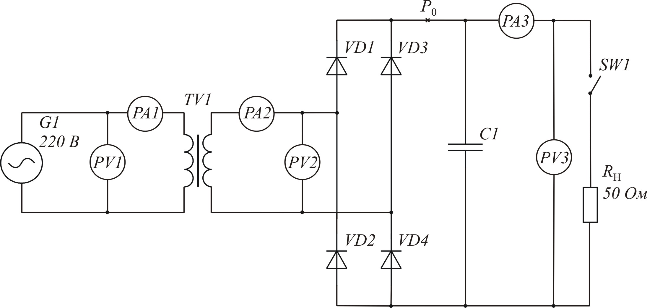
Picture 3.4 – Scheme of rectification with active-capacitive load (k = 3)
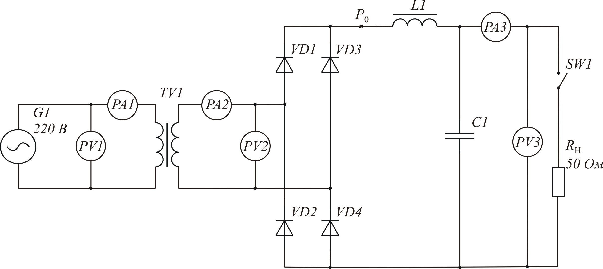
Picture 3.5 – Scheme of rectification with Г-type LC filter (k = 4)
