

1.2.4. Базовый командный файл для части в

# *************************************************************************** #
# #
# --- <<< Lab_2b >>> --- #
# #
# *************************************************************************** #
graphics off
# ///////////////////////////// PROCESS HEADER \\\\\\\\\\\\\\\\\\\\\\\\\\\\\\\\
# ----- Selecting Models. -------------
implant tables=Default
pdbSet Silicon Dopant DiffModel Pair
# ----- Meshing Strategy. -------------
mgoals on min.normal.size=1<nm> max.lateral.size=50<nm> \
normal.growth.ratio=1.2 accuracy=0.1<nm>
# ----- Initial Grid. -----------------
line x loc=0 tag=Top spacing=0.05
line x loc=2 tag=Bottom spacing=0.05
line y loc=0 tag=Mid spacing=0.025
line y loc=@<Lg*0.001/2+0.3>@ tag=Right spacing=0.025
# ----- Substrate. --------------------
region Silicon xlo=Top xhi=Bottom ylo=Mid yhi=Right
init field=Phosphorus concentration=5.00e14 wafer.orient=100 slice.angle=-90
# ----- Saving Struct. ----------------
struct smesh=n@node@_0
# ///////////////////////////////// PROCESS \\\\\\\\\\\\\\\\\\\\\\\\\\\\\\\\\\\
# 1) ----- Screen Oxide. ----------------------------------------------------
deposit Oxide thickness=20<nm> type=anisotropic
# ----- Saving Struct. ----------------
struct smesh=n@node@_1
# 2) ----- P-well, Anti-punchthrough & Vt Adjustment Implants. --------------
implant Boron dose=2.00e13 energy=120 tilt=0 rotation=0
implant Boron dose=1.00e13 energy=50 tilt=0 rotation=0
implant Boron dose=1.00e13 energy=25 tilt=0 rotation=0
# 3) ----- P-well: RTA of Channel Implants. ---------------------------------
diffuse time=10<s> temp=1050
# ----- Saving Struct. ----------------
struct smesh=n@node@_3
# 4) ----- Clean PAD Oxide. -------------------------------------------------
etch Oxide thickness=22<nm> type=anisotropic
# ----- Saving Struct. ----------------
struct smesh=n@node@_4
# 5) ----- Gate Oxidation. --------------------------------------------------
deposit Oxide thickness=1.2<nm> type=anisotropic
# ----- Saving Struct. ----------------
struct smesh=n@node@_5
# 6) ----- Poly Gate Deposition. --------------------------------------------
deposit PolySilicon thickness=0.14 type=anisotropic
mask name=gate_mask left=-1 right=@<Lg*0.001/2>@
etch Poly thickness=0.16 mask=gate_mask type=anisotropic
etch Oxide thickness=0.1 type=anisotropic
# ----- Saving Struct. ----------------
struct smesh=n@node@_6
# 7) ----- Poly Reoxidation. ------------------------------------------------
gas_flow name=flow_1 flowN2=0.99 flowO2=0.01
diffuse time=10 temp=900 gas_flow=flow_1
# ----- Saving Struct. ----------------
struct smesh=n@node@_7
# 8) ----- Reflect Before Halo. ---------------------------------------------
transform reflect left
# ----- Saving Struct. ----------------
struct smesh=n@node@_8
# 9) ----- N-LDD Implantation. ----------------------------------------------
implant Arsenic dose=8.00e14 energy=5 tilt=0 rotation=0 ifactor=0.1
# 10) ----- Halo Implantation: Quad HALO Implants. ---------------------------
implant Boron dose=6.00e13 energy=10 tilt=30 rotation=0 mult.rot=4 ifactor=0.1
# 11) ----- Structure Cut. ---------------------------------------------------
transform cut left loc=0
# ----- Saving Struct. ----------------
struct smesh=n@node@_11
# 12) ----- RTA of LDD/HALO Implants. ----------------------------------------
diffuse time=1<s> temp=1000 init=1e-8
# ----- Saving Struct. ----------------
struct smesh=n@node@_12
# 13) ----- Nitride Spacer. --------------------------------------------------
deposit Oxide thickness=0.01 type=isotropic
deposit Nitride thickness=0.025 type=isotropic
deposit Oxide thickness=0.01 type=isotropic
etch Oxide thickness=0.05 type=anisotropic
etch Oxide thickness=0.001 type=isotropic
etch Nitride thickness=0.06 type=anisotropic
etch Nitride thickness=0.001 type=isotropic
etch Oxide thickness=0.008 type=anisotropic
# ----- Saving Struct. ----------------
struct smesh=n@node@_13
# 14) ----- N+ implantation. -------------------------------------------------
implant spec=Phosphorus damage
implant Phosphorus dose=1.50e15 energy=20 tilt=0 rotation=0 ifactor=0.1
# 15) ----- Final RTA. -------------------------------------------------------
diffuse time=1<s> temp=1025 init=1e-8
# ----- Saving Struct. ----------------
struct smesh=n@node@_15
# 16a) ----- #split <Strain> --------------------------------------------------
etch Oxide thickness=30<nm> type=isotropic
deposit Oxynitride thickness=75<nm> type=isotropic
# ----- Saving Struct. ----------------
struct smesh=n@node@_16a
# 16b) ------------------------------------------------------------------------
#if @<Strain == 1>@
stress Oxynitride sxxi=@Sxx@e9<Pa> syyi=@Syy@e9<Pa> szzi=@Szz@e9<Pa>
# ----- Saving Struct. ----------------
struct smesh=n@node@_16b
#endif
# 16c) ----- Recompute the Stress Distribution. -------------------------------
pdbSet Silicon Dopant DiffModel Constant
diffuse time=1e-10 temp=1025
# 17) ----- Final Reflect. ---------------------------------------------------
transform reflect left
# ----- Saving Struct. ----------------
struct smesh=n@node@_17
# ----- Saving Profiles. --------------
SetPlxList { Boron Arsenic Phosphorus NetActive }
WritePlx n@node@_CH y=0
WritePlx n@node@_SD y=@<Lg*0.001+0.25>@
# ----- RS Measuring. -----------------
SheetResistance y=0
SheetResistance y=@<Lg*0.001+0.25>@
# \\\\\\\\\\\\\\\\\\\\\\\\\\\\\\\\\ THE END ///////////////////////////////////
exit
Структура план вычислительного эксперимента, обеспечивающая вариации длины затвора, толщины cap-пленки и компонент тензора механических напряжений в cap-пленке, соответствует рисунку 2.3.
Двумерные профили легирования активной примеси на различных стадиях создания моделируемой структуры n-МОП нанотранзистора имеют вид, аналогичный рисунку 2.4.
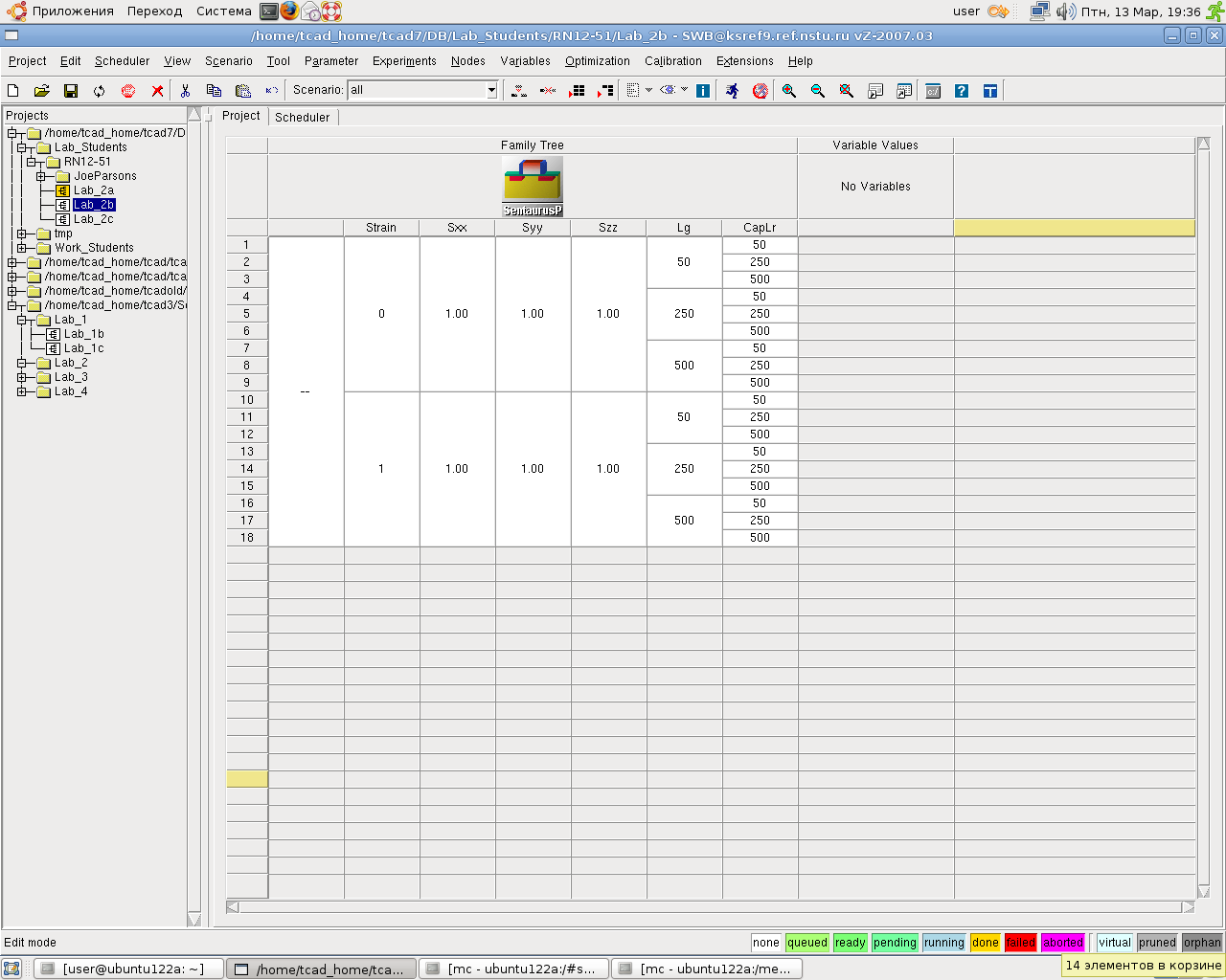
Рис. 2.3. Структура плана вычислительного эксперимента в оболочке SWB
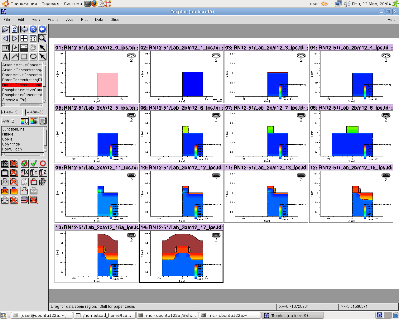
Рис. 2.4. Двумерные структуры, визуализирующие процесс создания n-МОП нанотранзистора на напряженном кремнии, полученные на основе командного файла для части B