

LABORATORY WORK #6
PHOTOCONDUCTIVITY PROPERTIES
OF SEMICONDUCTORS
PhysicVirtualLab Software Package
LABORATORY WORK #6
PHOTOCONDUCTIVITY PROPERTIES
OF SEMICONDUCTORS
1.AIM OF THE WORK:
Studying the phenomenon of photoconductivity of semiconductors
2.INTRODUCTION
1.1Inner photoeffect
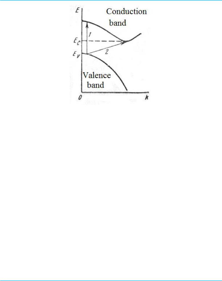
Inner photoelectric effect is a process of internal ionization of semiconductor under the influence of light, leading to the creation of additional, nonequilibrium charge carriers. Adding conductivity, caused by inner photoeffect called photoconductivity. At the inner photoeffect the primary process is the absorbtion of photons with sufficient energy to excite an electron into zone of conductivity (transitions 1 and 3, Figure 1) or on the local energy levels (transition 2, Figure 1) located in the band gap of the semiconductor. Transition 1 leads to the creation of electron-hole pairs, whereas in the results of those transitions 2 and 3, the charge carrier only one sign are created.
PhysicVirtualLabs Project Team, IITU
Copyright 2014

LABORATORY WORK #6
PHOTOCONDUCTIVITY PROPERTIES
OF SEMICONDUCTORS
PhysicVirtualLab Software Package
Figure 1 - Scheme of the possible optical transitions
in band gap
If the optical excitation of electrons happens from the valence band in the conduction band, the intrinsic photoconductivity is observed, which is created by the
charge carriers of both signs. Here, obviously, the photon energy |
should be less |
|
than the width of the band gap of the semiconductor |
. |
|
For the crystalline lattice is just the conservation of total wave number k, corresponding to the direct and indirect optical transitions. If the transition of an electron is at the interaction of photons and electrons, then the direct (vertical) optical transition happens (transition 1, Figure 2). However, in the crystal lattice a more complex process has a significant probability: the interaction of photons, electrons and phonons (quantum of the oscillations of the crystal lattice). As a result of this interaction the electron has in general the energy of the photon and changes its wave number because of the phonons (transition 2, Figure 2). Such transitions are called indirect (non-vertical) optical transitions.
PhysicVirtualLabs Project Team, IITU
Copyright 2014
LABORATORY WORK #6
PHOTOCONDUCTIVITY PROPERTIES
OF SEMICONDUCTORS
PhysicVirtualLab Software Package
Figure 2 - Direct 1 and nondirect 2 optical interband transitions
At the complex energy zone to the direct optical transitions may correspond the energy greater than the energy of thermal transitions. Since the probability of indirect optical transitions is less probability of direct transitions, in the absorption spectra of the photon energy corresponding to direct transitions should be observed more or less sharp increase in absorption and, therefore, the photoconductivity.
Own absorption band, having always a distinct long-wave border, in principle, can have shorter border. However, in many cases, the conduction band overlaps by the overlying allowed bands, making a continuous spectrum. Therefore, the absorption spectrum and the spectral dependence of the inner photoelectric effect extend to the far short wave range. However, at higher photon energies ( ) phototransition of the electron in the conduction band can be followed by the effect of impact ionization, leading to the release of several electrons and holes. Thus, the theory of the inner photoelectric effect is reduced to the theory of absorption only in
PhysicVirtualLabs Project Team, IITU
Copyright 2014

LABORATORY WORK #6
PHOTOCONDUCTIVITY PROPERTIES
OF SEMICONDUCTORS
PhysicVirtualLab Software Package
some region of the spectrum near the long-wavelength edge of the fundamental absorption band.
2.2 Photoconductivity
Nonequilibrium electrons and holes, formed in the result of the interaction of high-energy photons, immediately after the ionization process can have energies larger than the average energy of equilibrium carriers, which is of order kT. However, in the result of the interaction with phonons and defects of crystalline lattice nonequilibrium carriers are gaining the lattice temperature rapidly, and their energy is equal to the average thermal energy of equilibrium charge carriers. This process occurs in a time of the order of 10-10 s, which is called the relaxation time of the charge carriers. Typically, the lifetime t of nonequilibrium charge carriers exceeds this value significantly, representing 10-2 – 10-7 s, and therefore most of the time before the recombination their kinetic energy corresponds to the mean thermal energy of equilibrium charge carriers. Therefore, we can assume that the energy distribution of nonequilibrium charge carriers in the zones is the same as the equilibrium. Hence the mobility μ nonequilibrium charge carriers has no difference from the mobility of equilibrium, because the mobility of electrons μn and holes μp are determined by the nature of interaction of the charge carriers with lattice and depends, in particular, the distribution of the energy carriers.
Thus, the generation of charge carriers under the light leads to the changes of the electrical conductivity σ semiconductor, which at the presence of nonequilibrium electrons Δn and holes Δp can be written as
|
|
[( |
) |
( |
) ], (1) |
where |
и |
are equilibrium concentrations of electrons and holes. |
|||
Excess (nonequilibrium) conductivity, equals to the difference between the conductivity of semiconductors in the presence (σ) and absence (σ0) of lighting, is a photoconductivity (σф):
PhysicVirtualLabs Project Team, IITU
Copyright 2014

LABORATORY WORK #6
PHOTOCONDUCTIVITY PROPERTIES
OF SEMICONDUCTORS
|
PhysicVirtualLab Software Package |
|
|
( |
), (2) |
Naturally, the concentration of nonequilibrium carriers Δn and Δp depend on the intensity and duration of semiconductor lighting.
Denote the rate of generation of charge carriers under illumination as Δn' and Δp'.
Obviously, Δn' and Δp' should be proportional to the light energy, absorbing in unit per volume of the semiconductor for unit per time. If the intensity of monochromatic light of layer of thickness dx is equal to I, and the absorption coefficient is equal to k, then the amount of light energy, absorbing in unit per time in unit per volume is equal to:
.
Thus, the rate of generation of carriers Δn' and Δp' is proportional to kI. For the fundamental absorption
. (3)
The coefficient of proportionality is called the coefficient in the quantum yield, as it determines the number of pairs of charge carriers (or the number of charge carriers in the impurity photoconductivity) formed by one of the absorbed quantum of light, if the light intensity I measured by the number of photons per second. Usually, the quantum yield coefficient does not exceed unity.
Under the continuous illumination of the semiconductor by light of constant intensity there is the stationary state, characterizing by the constant concentration of nonequilibrium charge Δn and Δp.
Let’s find the dependence of Δn and Δp on time t and define the steady-state values of the nonequilibrium charge carriers, considering the intensity of light is constant over the entire volume of the sample, which leads to a homogeneous carrier generation.
Immediately after the start of illumination, at the increase of the concentration of nonequilibrium charge carriers the intensity of the recombination process begin to
PhysicVirtualLabs Project Team, IITU
Copyright 2014

LABORATORY WORK #6
PHOTOCONDUCTIVITY PROPERTIES
OF SEMICONDUCTORS
PhysicVirtualLab Software Package
increase. Since the rate of generation of nonequilibrium charge carriers is constant at a constant at the constant light intensity, the intensity of recombination reaches soon the intensity of the generation of carriers, and a steady state of nonequilibrium concentration of photocarriers stays.
Change in the concentration of nonequilibrium carriers in the unit of time is the difference between the rates of generation and recombination of carriers:
. (4)
The second term of the right side of equation (4) takes into account the decrease in the concentration of minority charge carriers in the result of the recombination process. The rate of recombination can be considered proportional to the concentration of nonequilibrium carriers only if the lifetime of nonequilibrium carriers (the same for electrons and holes) does not depend on their concentration.
This condition occurs when the concentration of nonequilibrium carriers Δn, Δp is small compared to the equilibrium concentration of the majority charge carriers (example Δn = Δp << p0), since this change in the concentration of majority carriers under illumination can be ignored and consider it as a constant. This occurs, for example, in doped semiconductor at the generation of photocarriers in the fundamental absorption at a temperature such that all the impurities are ionized.
We find the solution of equation (4), assuming that Δn = Δp << p0 and p0 >> n0 and the semiconductor starts illuminate at time t = 0 by the light of constant intensity. Then, separating the variables and integrating with the initial condition Δn = 0 for t = 0, we obtain
|
( |
). (5) |
Set value of the nonequilibrium electron density Δn0 is determined from equation |
||
(5) at |
: |
|
|
|
. (6) |
PhysicVirtualLabs Project Team, IITU
Copyright 2014

LABORATORY WORK #6
PHOTOCONDUCTIVITY PROPERTIES
OF SEMICONDUCTORS
PhysicVirtualLab Software Package
If, on the contrary, in the sample the nonequilibrium steady state concentration Δn0 are created and at t = 0 the light is off, the concentration of nonequilibrium charge carriers drops to zero by the law
. (7)
Thus, the relaxation (i.e., the rise and fall) of the nonequilibrium charge carrier concentration at instant light switch is exponential function with a time constant , corresponding to the lifetime of nonequilibrium charge carriers.
The obtained analytical dependence for the growth of nonequilibrium charge carriers leads to determine the law of change of the nonequilibrium stationary conductivity (concentration) on the illumination intensity, i.e., the so-called luxampere characteristics. At the linear recombination law, when the lifetime of nonequilibrium charge carriers doesn’t depend on the intensity of light, lux-ampere characteristic is linear, as in accordance with equation (6), the stationary nonequilibrium concentration Δn0 is proportional to the light intensity I.
3. EXPERIMENTS DESCRIPTION
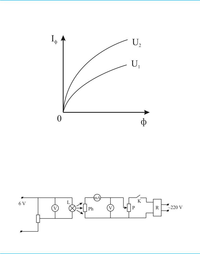
Photoresistivity (photoresistor) is semiconductor device, in which conductivity can be changed due to lightening. Photoresistor is thin layer of semiconductor 2, which is put on insulated substrate 1 and located between electrodes 3 (see in Figure 3). Receiving part of photoresistor is covered by layer of transparent varnish and has square or circle form.
If photoresistor is turned on in series with source and is not lightened, in the circuit will flow the dark current.
, (8)
where В is coefficient, defined by geometrical forms of photosensitive layer; U is voltage applied on photoresistor.
PhysicVirtualLabs Project Team, IITU
Copyright 2014

LABORATORY WORK #6
PHOTOCONDUCTIVITY PROPERTIES
OF SEMICONDUCTORS
PhysicVirtualLab Software Package
a
b
Figure 3- Photo resistor and scheme of turning on
During the lightening of photoresistor, conductivity of photosensitive layer increases according to (1) and photoelectric current flows through device, which is
PhysicVirtualLabs Project Team, IITU
Copyright 2014
LABORATORY WORK #6
PHOTOCONDUCTIVITY PROPERTIES
OF SEMICONDUCTORS
PhysicVirtualLab Software Package
equal to sum of dark current Id and photoelectric current Iф. Photoelectric current is defined:
. (9)
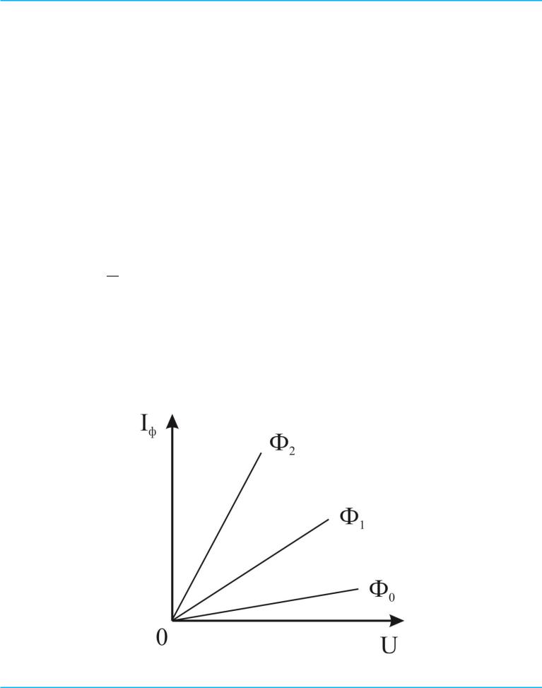
Main properties of photoresistivity is current–voltage characteristic, optical characteristics, spectral characteristics. Current–voltage characteristic represents dependence of photoelectric current IФ on voltage U at constant light flux Ф or illumination E= Ф/S.
This dependence according to (9) has linear character, i.e. can be described by
Ohm’s law (Figure 4).
Optical characteristics presents dependence of photoelectric current IФ on flux Ф (or illumination) at constant voltage of photoresistor. At low flux photoelectric current is √ (Figure 4, b). Spectral characteristics gives dependence of device’s sensitivity on wavelength ( ). Sensitivity of the device is defined by
. (10) |
|
Multiplicity of resistance measurement is equal to |
, i.e. relation of dark |
resistivity to resistivity with lightening at the same voltage. |
|
PhysicVirtualLabs Project Team, IITU
Copyright 2014
LABORATORY WORK #6
PHOTOCONDUCTIVITY PROPERTIES
OF SEMICONDUCTORS
PhysicVirtualLab Software Package
a
b
Figure 4 - Current–voltage characteristics
Experimental setup is presented in Figure 5. It consists of electric scheme of turning on for photoresistor, here P is potentiometer, voltage from rectifier R is applied on the potentiometer. Lightening of photoresistor occurs due to glow lamp L, which is connected to direct current source (6V).
Figure 5 - Experimental setup
PhysicVirtualLabs Project Team, IITU
Copyright 2014