


2 Theory of operation
In most of the literature, permanent magnet motors are divided into two categories based on the shape of the back-EMF (voltage induced in the coils when the motor is spinning). The back-EMF can either be trapezoidal or sinusoidal in shape. Although the terminology is not consistent throughout the literature, the majority seems to agree that a brushless DC motor (BLDC) has trapezoidal back-EMF, while a permanent magnet synchronous motor (PMSM) has sinusoidal back-EMF. Both BLDC and PMSM motors can be driven by sinusoidal currents, so there will not be made any distinction between them throughout this application note. Instead, they will both be referred to as a permanent magnet motor, or PMM.
3 Implementation on an AVR®
This application note describes how to drive a three-phase PMM with sinusoidal currents. The code example can also be used as a general reference on how to generate waveforms using the PWM.
3.1 Voltage generation
In order to drive a three-phase motor with sinusoidal currents, independent voltages for each phase must be generated. The driver stage for a three-phase motor usually consists of three half-bridges, one for each terminal. Each half-bridge consists of two switches, e.g. two power MOSFET transistors. To understand how the phase voltages are generated, it is sufficient to look at one half-bridge. Figure 3-1 shows one half-bridge connected to a DC voltage source.
Figure 3-1. Voltage generation using a half-bridge.
|
|
|
|
|
PWMH |
|
|
|
|||
VD |
|
|
|
|
VOUT |
C |
|
|
|
|
|
|
|
|
|
|
PWML |
3.1.1 PWM
The average voltage of the output, VOUT, can be regulated between 0V and VDC by applying two inverted pulse-width modulated (PWM) signals to the two switches,
PWMH and PWML. The average output voltage will be proportional to the duty cycle of the high side switch. The output, VOUT, will in this case not be a smooth voltage curve, but a square wave similar in shape to the PWM signal applied to the high side switch. If this signal were fed through a low-pass filter, the output voltage would be a voltage level proportional to the duty cycle of the high side switch.
2 AVR447
8010A-AVR-06/06

AVR447
For several reasons, it is not common to add a separate low-pass filter in motor control designs. First of all, the motor acts as a low pass filter. The inductance and resistance of the coils windings create a low pass RL filter. Further, the inertia of the rotor and load creates a mechanical low pass filter. Choosing the PWM switching frequency sufficiently high, there will be no noticeable jitter in the rotor speed. Secondly, the currents fed through the windings of even a small motor can be in the range of several amperes. Forcing this current through e.g. an RC filter would result in substantial power dissipation in the filter itself, an undesirable energy loss.
3.1.2 Dead-time
Switching devices, such as MOSFET transistors are not able to switch on and off instantly. Consider again the half-bridge from Figure 3-1. If the switches PWMH and PWML are fed with inverted signals, one switch will turn off at the same moment as the other switch turns on. During this transition, there will be a short time period where one switch has not completely closed while the other one is opening, making a direct connection between supply voltage and ground with very low resistance, allowing a large current to flow through the transistors. This situation is known as a shoot-through, and must be avoided, since it will probably destroy the driver stage if no hardware protection is in place.
The solution to this is to add a dead-time, a small time period where neither the high or low side switches are conducting, for every PWM transition.
3.1.3 Generating PWM signals with dead-time with an AVR
To understand how to implement PWM “voltage generation” with dead-time on an AVR, we continue to look at only one phase voltage. One timer/counter module on e.g. the ATmega48 can be used to control one half-bridge like the one in Figure 3-1. The timer/counter modules in the ATmega48 can control two PWM output pins each. The timer/counter units have several PWM modes, and there are several configuration options for the output pins.
For the half-bridge control with dead-time, the phase correct PWM mode is very well suited. The counter works in a dual slope mode, which allows generation of centeraligned PWM signals with dead-time. Consider Figure 3-2 that shows how Timer/Counter0 can be set up to produce the desired signals. The triangular line represents the timer/counter value itself in the dual slope “phase correct mode”. In this example, the output pin OC0A has been configured to clear on compare match when up-counting and set on compare match when down-counting. This output will be connected to the high side switch of the half-bridge. Similarly, the output pin OC0B has been configured to set on compare match when up-counting and clear on compare match when down-counting. This output will be connected to the low-side switch of the half-bridge. Note that if the compare values for both outputs are set to the same value, the two outputs will be complementary. However, to insert a deadtime between the switching of the low and high side drivers, the compare values must be moved a little bit in each direction. Half the dead-time is subtracted from the OC0A compare value while the same amount is added to the OC0B compare value. This is illustrated by the short horizontal lines on the timer/counter curve in Figure 3-2. As can be seen from the OC0A and OC0B waveforms, the effect is that a dead-time of the same length is inserted at every PWM switching.
3
8010A-AVR-06/06
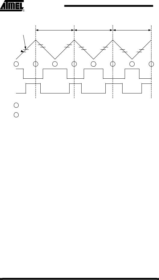
Figure 3-2. Generating complementary PWM signals with dead-time.
PWM cycle
OC0B compare value
TOP
OC0 compare value 
TCNT0
1 |
2 |
1 |
2 |
1 |
2 |
1 |
2 |
OC0A
OC0B
1Timer/counter overflow flag set
2Output compare values updated
To avoid accidental shoot-through when the compare values are changed, it is very important that the compare values for both OC0A and OC0B are updated at the same exact time. This is accomplished through the double buffering of compare registers and the interrupt functionality of the AVR timer/counter units. In Figure 3-2, each PWM cycle is marked with dashed lines. When running in phase correct PWM mode, the compare values for the two outputs will be effective from the moment marked with a 2 in Figure 3-2. At the moment marked 1, the timer/counter overflow flag will be set. This can be used to run a periodic interrupt where the output compare values can be updated. If the 16-bit Timer/counter1 is used, it can be configured to use the input capture register as the top value for the counter. A capture event interrupt will then be triggered at the same time as the output compare values are updated. Using this interrupt instead of the overflow interrupt doubles the clock cycles available to compute new output compare values. Since all Timer/counter units are used in this application, the capture event interrupt is used.
3.1.4 PWM base frequency
When an 8-bit timer/counter unit is used to produce two PWM outputs with different compare values, the top value will be fixed at 255. The 16 bit timer/counter unit must be set in 8 bit phase correct PWM mode to behave like the 8 bit timer/counter units. In phase correct mode, one PWM cycle with a top value of 255 will have a period of 510 timer clock cycles, or 510 CPU clock cycles, assuming a clock percale value of 1 is used. The PWM frequency as a function of CPU frequency can be calculated from Equation 3-1.
4 AVR447
8010A-AVR-06/06