

Philips Semiconductors |
Product specification |
|
|
Hex inverting Schmitt trigger |
74HC14; 74HCT14 |
|
|
MNA850
1.8 handbook, halfpage
ICC (mA)
1.5
1.2
0.9
0.6
0.3
0
0 |
1 |
2 |
3 |
4 |
5 |
6 |
VI (V)
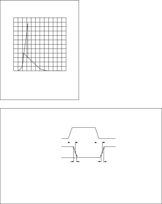
VCC = 5.5 V.
Fig.13 Typical 74HCT14 transfer characteristics.
AC WAVEFORMS
VI |
|
|
|
|
|
|
|
|
|
|
|
|
|
|
|
|
|
|
VM |
|
|
VM |
|||||||||
nA input |
|
|
|
|
|||||||||||
|
|
|
|
||||||||||||
GND |
|
|
|
|
|
|
|
|
|
|
|
|
|
||
|
|
|
|
|
|
|
|
tPHL |
|
|
|
|
|
|
tPLH |
|
|
|
|
|
|
|
|
|
|
|
|
|
|
||
VOH |
|
90% |
|
|
|
nY output |
VM |
VM |
VOL |
|
10% |
|
|
tTHL |
tTLH |
MNA722 |
74HC14: VM = 50%; VI = GND to VCC. 74HCT14: VM = 1.3 V; VI = GND to 3.0 V.
Fig.14 The input (nA) to output (nY) propagation delays and output transitions times.
2003 Oct 30 |
15 |

Philips Semiconductors |
Product specification |
|
|
Hex inverting Schmitt trigger |
74HC14; 74HCT14 |
|
|
|
|
S1 |
VCC |
|
VCC |
|
open |
|
RL = |
GND |
|
|
|
||
VI |
VO |
1 kΩ |
|
PULSE |
D.U.T. |
|
|
GENERATOR |
|
|
|
|
CL = |
|
|
RT |
|
|
|
|
50 pF |
|
|
|
|
MNA742 |
|
TEST S1
tPLH/tPHL open
tPLZ/tPZL VCC
tPHZ/tPZH GND
Definitions for test circuit: RL = Load resistor.
CL = load capacitance including jig and probe capacitance.
RT = termination resistance should be equal to the output impedance Zo of the pulse generator.
Fig.15 Load circuitry for switching times.
2003 Oct 30 |
16 |

Philips Semiconductors |
Product specification |
|
|
Hex inverting Schmitt trigger |
|
|
74HC14; 74HCT14 |
||
APPLICATION INFORMATION |
|
|
|
|
|
The slow input rise and fall times cause additional power |
400 |
|
|
MNA852 |
|
dissipation. This can be calculated using the following |
|
|
|
|
|
handbook, halfpage |
|
|
|
||
formula: |
ICC(AV) |
|
|
|
|
Pad = fi × (tr × ICC(AV) + tf × ICC(AV)) × VCC. |
( A) |
|
|
|
|
300 |
|
|
|
|
|
|
|
|
|
|
|
Where: |
|
|
|
|
|
Pad = additional power dissipation (μW); |
|
|
|
|
|
fi = input frequency (MHz); |
200 |
|
positive - going |
|
|
tr = input rise time (μs); 10% to 90%; |
|
|
edge |
|
|
|
|
|
|
|
|
tf = input fall time (μs); 10% to 90%; |
|
|
|
|
|
ICC(AV) = average additional supply current (μA). |
100 |
|
|
|
|
ICC(AV) differs with positive or negative input transitions, as |
|
|
negative - going |
|
|
shown in Figs 16 and 17. |
|
|
|
||
|
|
|
edge |
|
|
For 74HC/HCT14 used in a relaxation oscillator circuit, |
0 |
2 |
4 |
|
6 |
0 |
VCC (V) |
||||
see Fig.18. |
|
|
|
|
|
|
|
|
|
|
|
Note to application information |
|
|
|
|
|
All values given are typical unless otherwise specified. |
Linear change of VI between 0.1VCC to 0.9VCC |
|
|
||
|
|
|
|
|
|
|
Fig.16 |
Average ICC for 74HC14 Schmitt trigger |
|||
|
|
devices. |
|
|
|
400 |
|
|
|
|
MNA853 |
handbook, halfpage |
|
|
|
|
|
ICC(AV) |
|
|
|
|
|
( A) |
|
|
|
|
positive - going |
300 |
|
|
|
|
|
|
|
|
|
|
edgegde |
200 |
|
|
|
|
|
|
|
|
|
|
|
|
|
|
|
|
|
|
|
|
|
|
|
|
|
|
|
negative - going |
|
100 |
|
|
|
|
edgegde |
|
|
|
|
|
|
0 |
|
|
|
|
|
|
|
|
|
|
|
|
|
|
|
|
|
0 |
2 |
|
4 VCC (V) 6 |
||
Linear change of VI between 0.1VCC to 0.9VCC.
Fig.17 Average ICC for HCT Schmitt trigger devices.
R
C 
MNA854
74HC14 : f = |
---1 |
≈ |
------------------ |
1 |
|
T |
|
0.8 RC |
|
74HCT14 : f = |
---1 |
≈ |
---------------------1 |
|
|
|
T |
|
0.67 RC |
Fig.18 Relaxation oscillator using 74HC/HCT14.
2003 Oct 30 |
17 |

Philips Semiconductors |
Product specification |
|
|
Hex inverting Schmitt trigger |
74HC14; 74HCT14 |
|
|
PACKAGE OUTLINES |
|
SO14: plastic small outline package; 14 leads; body width 3.9 mm |
SOT108-1 |
D |
|
E |
A |
|
|
|
|
|
X |
|
c |
|
|
|
y |
|
HE |
|
v M A |
|
|
|
||
Z |
|
|
|
|
14 |
8 |
|
|
|
|
|
Q |
|
|
|
|
A2 |
(A3) |
A |
|
|
A1 |
||
pin 1 index |
|
|
|
|
|
|
|
|
θ |
|
|
L p |
|
|
1 |
7 |
L |
|
|
|
|
|
||
e |
w M |
detail X |
|
|
|
bp |
|
|
|
|
|
|
|
|
|
|
0 |
|
2.5 |
|
5 mm |
|
|
|
|
|
|
|
|
||||
|
|
|
|
|
|
|
|
|
|
|
|
|
|
|
|
|
|
|
|
|
|
|
|
|
|
|
|
|
|
|
|
|
|
scale |
|
|
|
|
|
|
|
|
|
|
|
||
DIMENSIONS (inch dimensions are derived from the original mm dimensions) |
|
|
|
|
|
|
|
|
|
|
|||||||||||||
|
|
|
|
|
|
|
|
|
|
|
|
|
|
|
|
|
|
|
|
|
|
|
|
UNIT |
A |
A1 |
A2 |
A3 |
bp |
c |
D(1) |
E(1) |
e |
HE |
|
L |
Lp |
Q |
v |
w |
y |
Z (1) |
θ |
|
|||
max. |
|
|
|||||||||||||||||||||
|
|
|
|
|
|
|
|
|
|
|
|
|
|
|
|
|
|
|
|
|
|
||
|
|
|
|
|
|
|
|
|
|
|
|
|
|
|
|
|
|
|
|
|
|
|
|
mm |
1.75 |
0.25 |
1.45 |
0.25 |
0.49 |
0.25 |
8.75 |
4.0 |
1.27 |
6.2 |
1.05 |
1.0 |
0.7 |
0.25 |
0.25 |
0.1 |
0.7 |
|
|
||||
0.10 |
1.25 |
0.36 |
0.19 |
8.55 |
3.8 |
5.8 |
0.4 |
0.6 |
0.3 |
8 |
o |
||||||||||||
|
|
|
|
|
|
|
|
|
|
||||||||||||||
|
|
|
|
|
|
|
|
|
|
|
|
|
|
|
|
|
|
|
|
|
0o |
||
inches |
0.069 |
0.010 |
0.057 |
0.01 |
0.019 |
0.0100 |
0.35 |
0.16 |
0.05 |
0.244 |
0.041 |
0.039 |
0.028 |
0.01 |
0.01 |
0.004 |
0.028 |
||||||
0.004 |
0.049 |
0.014 |
0.0075 |
0.34 |
0.15 |
0.228 |
0.016 |
0.024 |
0.012 |
|
|
||||||||||||
|
|
|
|
|
|
|
|
|
|
|
|
|
|
|
|
|
|
|
|
|
|
|
|
Note
1. Plastic or metal protrusions of 0.15 mm (0.006 inch) maximum per side are not included.
OUTLINE |
|
REFERENCES |
|
EUROPEAN |
ISSUE DATE |
|||||||||||
VERSION |
IEC |
JEDEC |
JEITA |
|
|
PROJECTION |
||||||||||
|
|
|
|
|||||||||||||
|
|
|
|
|
|
|
|
|
|
|
|
|
|
|||
|
|
|
|
|
|
|
|
|
|
|
|
|
|
|
|
|
SOT108-1 |
076E06 |
MS-012 |
|
|
|
|
|
|
|
|
|
|
|
|
99-12-27 |
|
|
|
|
|
|
|
|
|
|
|
|
|
|
||||
|
|
|
|
|
|
|
|
|
|
|
|
|||||
|
|
|
|
|
|
|
|
|
|
|
|
03-02-19 |
|
|||
|
|
|
|
|
|
|
|
|
|
|
|
|
|
|
|
|
|
|
|
|
|
|
|
|
|
|
|
|
|
|
|
|
|
2003 Oct 30 |
18 |

Philips Semiconductors |
Product specification |
|
|
Hex inverting Schmitt trigger |
74HC14; 74HCT14 |
|
|
DIP14: plastic dual in-line package; 14 leads (300 mil) |
SOT27-1 |
seating plane
|
D |
|
ME |
|
|
A2 |
A |
L |
|
A1 |
|
|
|
|
c |
Z |
e |
w M |
|
|
|
b1 |
|
|
|
b |
(e1) |
|
|
|
|
|
14 |
8 |
MH |
pin 1 index
E
1 |
7 |
0 |
5 |
10 mm |
scale
DIMENSIONS (inch dimensions are derived from the original mm dimensions)
UNIT |
A |
A1 |
A 2 |
b |
b |
1 |
c |
D |
(1) |
E |
(1) |
e |
e |
1 |
L |
M |
E |
M |
H |
w |
Z (1) |
|
max. |
min. |
max. |
|
|
max. |
|||||||||||||||||
|
|
|
|
|
|
|
|
|
|
|
|
|
|
|||||||||
|
|
|
|
|
|
|
|
|
|
|
|
|
|
|
|
|
||||||
mm |
4.2 |
0.51 |
3.2 |
1.73 |
0.53 |
0.36 |
19.50 |
6.48 |
2.54 |
7.62 |
3.60 |
8.25 |
10.0 |
0.254 |
2.2 |
|||||||
1.13 |
0.38 |
0.23 |
18.55 |
6.20 |
3.05 |
7.80 |
8.3 |
|||||||||||||||
|
|
|
|
|
|
|
|
|
||||||||||||||
|
|
|
|
|
|
|
|
|
|
|
|
|
|
|
|
|
||||||
inches |
0.17 |
0.02 |
0.13 |
0.068 |
0.021 |
0.014 |
0.77 |
0.26 |
0.1 |
0.3 |
0.14 |
0.32 |
0.39 |
0.01 |
0.087 |
|||||||
0.044 |
0.015 |
0.009 |
0.73 |
0.24 |
0.12 |
0.31 |
0.33 |
|||||||||||||||
|
|
|
|
|
|
|
|
|
||||||||||||||
|
|
|
|
|
|
|
|
|
|
|
|
|
|
|
|
|
|
|
|
|
|
|
Note
1. Plastic or metal protrusions of 0.25 mm (0.01 inch) maximum per side are not included.
OUTLINE |
|
REFERENCES |
|
EUROPEAN |
ISSUE DATE |
|||||||||||
VERSION |
IEC |
JEDEC |
JEITA |
|
|
PROJECTION |
||||||||||
|
|
|
|
|||||||||||||
|
|
|
|
|
|
|
|
|
|
|
|
|
|
|||
|
|
|
|
|
|
|
|
|
|
|
|
|
|
|
|
|
SOT27-1 |
050G04 |
MO-001 |
SC-501-14 |
|
|
|
|
|
|
|
|
|
|
|
99-12-27 |
|
|
|
|
|
|
|
|
|
|
|
|
|
|||||
|
|
|
|
|
|
|
|
|
|
|
||||||
|
|
|
|
|
|
|
|
|
|
|
03-02-13 |
|
||||
|
|
|
|
|
|
|
|
|
|
|
|
|
|
|
|
|
|
|
|
|
|
|
|
|
|
|
|
|
|
|
|
|
|
2003 Oct 30 |
19 |

Philips Semiconductors |
Product specification |
|
|
Hex inverting Schmitt trigger |
74HC14; 74HCT14 |
|
|
TSSOP14: plastic thin shrink small outline package; 14 leads; body width 4.4 mm |
SOT402-1 |
D |
|
E |
A |
|
|
|
X |
|
c |
|
|
y |
|
HE |
v M A |
|
|
||
Z |
|
|
|
14 |
8 |
|
|
|
|
|
Q |
|
A |
2 |
(A3) |
|
|
A |
|
pin 1 index |
|
A1 |
|
|
|
|
θ |
|
|
|
Lp |
|
|
L |
|
1 |
7 |
|
|
|
w M |
detail X |
|
|
|
|
|
e |
bp |
|
|
|
|
|
|
|
|
|
|
0 |
|
2.5 |
|
5 mm |
|
|
|
|
|
|
|
|||
|
|
|
|
|
|
|
|
|
|
|
|
|
|
|
|
|
|
|
|
|
|
|
|
|
|
|
|
|
|
|
|
|
|
scale |
|
|
|
|
|
|
|
|
|
|
|
DIMENSIONS (mm are the original dimensions) |
|
|
|
|
|
|
|
|
|
|
|
|
|
|
|
|
||||||
|
|
|
|
|
|
|
|
|
|
|
|
|
|
|
|
|
|
|
|
|
|
|
UNIT |
A |
A1 |
A2 |
A3 |
bp |
|
c |
D (1) |
E (2) |
|
e |
HE |
|
L |
Lp |
Q |
v |
w |
y |
Z (1) |
θ |
|
max. |
|
|
|
|||||||||||||||||||
|
|
|
|
|
|
|
|
|
|
|
|
|
|
|
|
|
|
|
|
|
|
|
|
|
|
|
|
|
|
|
|
|
|
|
|
|
|
|
|
|
|
|
|
|
|
mm |
1.1 |
0.15 |
0.95 |
0.25 |
0.30 |
|
0.2 |
5.1 |
4.5 |
0.65 |
6.6 |
1 |
0.75 |
0.4 |
0.2 |
0.13 |
0.1 |
0.72 |
8o |
|||
0.05 |
0.80 |
0.19 |
|
0.1 |
4.9 |
4.3 |
6.2 |
0.50 |
0.3 |
0.38 |
0o |
|||||||||||
|
|
|||||||||||||||||||||
Notes
1.Plastic or metal protrusions of 0.15 mm maximum per side are not included.
2.Plastic interlead protrusions of 0.25 mm maximum per side are not included.
OUTLINE |
|
REFERENCES |
|
EUROPEAN |
ISSUE DATE |
|||||||||||
VERSION |
IEC |
JEDEC |
JEITA |
|
|
PROJECTION |
||||||||||
|
|
|
|
|||||||||||||
|
|
|
|
|
|
|
|
|
|
|
|
|
|
|||
|
|
|
|
|
|
|
|
|
|
|
|
|
|
|
|
|
SOT402-1 |
|
MO-153 |
|
|
|
|
|
|
|
|
|
|
|
|
99-12-27 |
|
|
|
|
|
|
|
|
|
|
|
|
|
|
|
|||
|
|
|
|
|
|
|
|
|
|
|
|
|
||||
|
|
|
|
|
|
|
|
|
|
|
|
|
03-02-18 |
|
||
|
|
|
|
|
|
|
|
|
|
|
|
|
|
|
|
|
|
|
|
|
|
|
|
|
|
|
|
|
|
|
|
|
|
2003 Oct 30 |
20 |
Philips Semiconductors |
Product specification |
|
|
Hex inverting Schmitt trigger |
74HC14; 74HCT14 |
|
|
DHVQFN14: plastic dual in-line compatible thermal enhanced very thin quad flat package; no leads; |
SOT762-1 |
14 terminals; body 2.5 x 3 x 0.85 mm |
D 

 B
B 
 A
A
|
A |
E |
A1 |
c |
|
terminal 1 |
detail X |
|
|
index area |
|
terminal 1 |
e1 |
|
|
|
|
C |
|
|
|
|
|
||
index area |
|
|
|
|
y1 C |
y |
e |
b |
v |
M C A B |
|||
2 |
|
w |
M |
C |
|
|
|
6 |
|
|
|
|
|
L |
|
|
|
|
|
|
1 |
|
7 |
|
|
|
|
Eh |
|
e |
|
|
|
|
14 |
|
8 |
|
|
|
|
13 |
|
9 |
|
|
|
|
|
Dh |
|
|
|
|
X |
|
|
|
|
|
|
|
0 |
|
2.5 |
|
|
5 mm |
|
scale
DIMENSIONS (mm are the original dimensions)
UNIT |
A(1) |
A1 |
b |
c |
D(1) |
Dh |
E(1) |
Eh |
e |
e1 |
L |
v |
w |
y |
y1 |
|
max. |
||||||||||||||||
|
|
|
|
|
|
|
|
|
|
|
|
|
|
|
|
|
mm |
1 |
0.05 |
0.30 |
0.2 |
3.1 |
1.65 |
2.6 |
1.15 |
0.5 |
2 |
0.5 |
0.1 |
0.05 |
0.05 |
0.1 |
|
0.00 |
0.18 |
2.9 |
1.35 |
2.4 |
0.85 |
0.3 |
||||||||||
|
|
|
|
|
|
|
|
|
||||||||
|
|
|
|
|
|
|
|
|
|
|
|
|
|
|
|
Note
1. Plastic or metal protrusions of 0.075 mm maximum per side are not included.
OUTLINE |
|
REFERENCES |
|
EUROPEAN |
ISSUE DATE |
|||||||||||
VERSION |
IEC |
JEDEC |
JEITA |
|
|
PROJECTION |
||||||||||
|
|
|
|
|||||||||||||
|
|
|
|
|
|
|
|
|
|
|
|
|
|
|||
|
|
|
|
|
|
|
|
|
|
|
|
|
|
|
|
|
SOT762-1 |
- - - |
MO-241 |
- - - |
|
|
|
|
|
|
|
|
|
|
|
02-10-17 |
|
|
|
|
|
|
|
|
|
|
|
|
|
|||||
|
|
|
|
|
|
|
|
|
|
|
||||||
|
|
|
|
|
|
|
|
|
|
|
03-01-27 |
|
||||
|
|
|
|
|
|
|
|
|
|
|
|
|
|
|
|
|
|
|
|
|
|
|
|
|
|
|
|
|
|
|
|
|
|
2003 Oct 30 |
21 |