

бакМИТ_КП2015 / Компоненты по вариантам / АЦП / AD7892
.pdfAD7892
The designed code transitions occur midway between successive integer LSB values (i.e., 1/2 LSB, 3/2 LSBs, 5/2 LSBs). Output coding is two’s complement binary with 1 LSB = FSR/4096 = 20 V/4096 = 4.88 mV for the ±10 V range and 1 LSB = FSR/ 4096 = 10 V/4096 = 2.44 mV for the ±5 V range. The ideal input/output transfer function for the AD7892-1 is shown in Table I.
AD7892-2
The analog input section for the AD7892-2 contains no biasing resistors. The analog input looks directly into the track/hold
input stage. The analog input range on the VIN1 input is 0 V to +2.5 V. The VIN2 input can be left unconnected but if it is connected to a potential then that potential must be AGND.
The VIN1 input connects directly to the input sampling capacitor of the AD7892-2’s track/hold. The value of this input sampling capacitor is nominally 10 pF.
Once again, the designed code transitions occur midway between successive integer LSB values (i.e., 1/2 LSB, 3/2 LSBs, 5/2 LSBs). Output coding is straight (natural) binary with
1 LSB = FSR/4096 = 2.5 V/4096 = 0.61 mV. The ideal input/ output transfer function for the AD7892-2 is shown in Table II.
Table I. Ideal Input/Output Code Table for the AD7892-1
|
Digital Output |
|
|
Analog Input |
Code Transition |
|
|
|
|
|
|
+FSR/2 – 3/2 LSB1, 2 (9.99268 or 4.99634)3 |
011 . . . |
110 to 011 . . . |
111 |
+FSR/2 – 5/2 LSBs (9.98779 or 4.99390) |
011 . . . |
101 to 011 . . . |
110 |
+FSR/2 – 7/2 LSBs (9.98291 or 4.99146) |
011 . . . |
100 to 011 . . . |
101 |
AGND + 3/2 LSB (0.00732 or 0.00366) |
000 . . . |
001 to 000 . . . |
010 |
AGND + 1/2 LSB (0.00244 or 0.00122) |
000 . . . |
000 to 000 . . . |
001 |
AGND – 1/2 LSB (–0.00244 or –0.00122) |
111 . . . |
111 to 000 . . . |
000 |
AGND – 3/2 LSB (–0.00732 or –0.00366) |
111 . . . |
110 to 111 . . . |
111 |
–FSR/2 + 5/2 LSB (–9.98779 or –4.99390) |
100 . . . |
010 to 100 . . . |
011 |
–FSR/2 + 3/2 LSB (–9.99268 or –4.99634) |
100 . . . |
001 to 100 . . . |
010 |
–FSR/2 + 1/2 LSB (–9.99756 or –4.99878) |
100 . . . |
000 to 100 . . . |
001 |
|
|
|
|
NOTES
1FSR is full-scale range and REF IN = +2.5 V, is 20 V for the ± 10 V range and 10 V for the ± 5 V range.
21 LSB = FSR/4096 = 4.88 mV (±10 V range) and 2.44 mV (± 5 V range) with REF IN = +2.5 V.
3± 10 V range or ±5 V range.
Table II. Ideal Input/Output Code Table for the AD7892-2
|
Digital Output |
|
|
Analog Input |
Code Transition |
|
|
|
|
|
|
+FSR – 3/2 LSB1, 2 (2.499084 V) |
111 . . . |
110 to 111 . . . |
111 |
+FSR – 5/2 LSBs (2.498474 V) |
111 . . . |
110 to 111 . . . |
110 |
+FSR – 7/2 LSBs (2.497864 V) |
111 . . . |
100 to 111 . . . |
101 |
AGND + 5/2 LSB (0.001526 V) |
000 . . . |
010 to 010 . . . |
011 |
AGND + 3/2 LSB (0.00916 V) |
000 . . . |
001 to 001 . . . |
010 |
AGND + 1/2 LSB (0.000305 V) |
000 . . . |
000 to 000 . . . |
001 |
|
|
|
|
NOTES
1FSR is full-scale range and is 2.5 V with REF IN = +2.5 V. 21 LSB = FSR/4096 = 0.61 mV with REF IN = +2.5 V.
AD7892-3
Figure 5 shows the analog input section for the AD7892-3. The
analog input range is ±2.5 V on the VIN1 input. The VIN2 input can be left unconnected but if it is connected to a potential then
that potential must be AGND. The input resistance on the VIN1 is 1.8 kΩ nominal. As a result, the VIN1 input should be driven from a low impedance source. The resistor attenuator stage is followed by the high input impedance stage of the track/hold amplifier. This resistor attenuator stage allows the input voltage to go to ±7 V without damaging the AD7892-3.
The designed code transitions occur midway between successive integer LSB values (i.e., 1/2 LSB, 3/2 LSBs, 5/2 LSBs). Output coding is two’s complement binary with 1 LSB = FSR/ 4096 = 5 V/4096 = 1.22 mV with REF IN = +2.5 V. The ideal input/output transfer function for the AD7892-3 is shown in Table III.
|
+2.5 |
|
2k |
REFERENCE |
|
|
|
|
REF OUT/ |
|
|
REF IN |
|
|
|
|
TO ADC |
|
|
REFERENCE |
|
3.25k |
CIRCUITRY |
3.25k |
|
TO HIGH |
VIN1 |
|
|
|
IMPEDANCE |
|
|
|
|
VIN2* |
|
SHA INPUT |
|
|
AGND 
* UNCONNECTED INTERNALLY ON THE AD7892-3
Figure 5. AD7892-3 Analog Input Structure
Table III. Ideal Input/Output Code Table for the AD7892-3
|
Digital Output |
|
|
Analog Input |
Code Transition |
|
|
|
|
|
|
+FSR/2 – 3/2 LSB1, 2 (2.49817) |
011 . . . |
110 to 011 . . . |
111 |
+FSR/2 – 5/2 LSBs (2.49695) |
011 . . . |
110 to 011 . . . |
110 |
+FSR/2 – 7/2 LSBs (2.49573) |
011 . . . |
110 to 011 . . . |
101 |
AGND + 3/2 LSB (0.00183) |
000 . . . |
001 to 000 . . . |
010 |
AGND + 1/2 LSB (0.00061) |
000 . . . |
000 to 000 . . . |
001 |
AGND – 1/2 LSB (–0.00061) |
111 . . . |
111 to 000 . . . |
000 |
AGND – 3/2 LSB (–0.00183) |
111 . . . |
110 to 111 . . . |
111 |
–FSR/2 + 5/2 LSB (–2.49695) |
100 . . . |
010 to 100 . . . |
011 |
–FSR/2 + 3/2 LSB (–2.49817) |
100 . . . |
001 to 100 . . . |
010 |
–FSR/2 + 1/2 LSB (–2.49939) |
100 . . . |
000 to 100 . . . |
001 |
|
|
|
|
NOTES
1FSR is full-scale range and is 5 V with REF IN = +2.5 V. 21 LSB = FSR/4096 = 1.22 mV with REF IN = +2.5 V.
REV. C |
–11– |
AD7892
MICROPROCESSOR INTERFACING
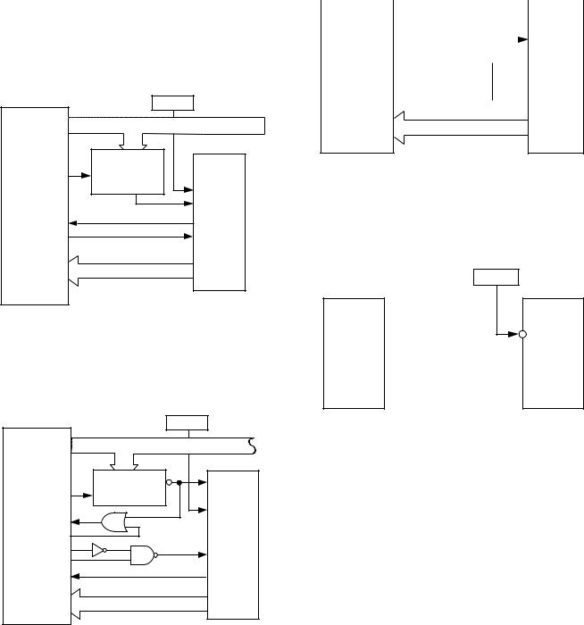
The AD7892 features both high speed parallel and serial interfaces, allowing considerable flexibility in interfacing to microprocessor systems. To obtain optimum performance from the part, data should not be read during conversion and this limits the achievable throughput rate in serial mode to 400 kSPS for the AD7892-3.
Figures 6, 7 and 9 show some typical interface circuits between the AD7892 and popular DSP processors. Figure 8 shows an interface between the part and a gate array or ASIC where data is clocked into the ASIC by the AD7892 itself at the end of conversion. In all cases, the CONVST signal is generated from an external timer to ensure equidistant sampling.
AD7892 to ADSP-2101 Interface
Figure 6 shows a parallel interface between the AD7892 and the ADSP-2101 DSP processor. CONVST starts conversion and at
the end of conversion the falling edge of the EOC output provides an interrupt request to the ADSP-2101.
|
|
TIMER |
DMA13–DMA0 |
ADDRESS BUS |
|
ADSP-2101 |
ADDRESS DECODE |
|
|
|
|
DMS |
LOGIC |
AD7892 |
EN |
|
|
|
|
CONVST |
|
|
CS |
IRQn |
|
EOC |
RD |
|
RD |
DMD15–DMD0 |
DATA BUS |
DB11–DB0 |
|
Figure 6. AD7892 to ADSP-2101
AD7892 to TMS320C25 Interface
Figure 7 shows a parallel interface between the AD7892 and the TMS320C25 DSP processor. CONVST starts conversion and at the end of conversion the falling edge of the EOC output provides an interrupt request to the TMS320C25.
|
|
TIMER |
A15–A0 |
ADDRESS BUS |
|
TMS320C25 |
ADDRESS DECODE |
|
|
CS |
|
|
LOGIC |
|
|
|
|
IS |
EN |
|
|
|
CONVST |
READY |
G2 |
|
MSC |
|
AD7892 |
|
|
|
STRB |
|
RD |
R/W |
|
|
|
|
|
INT |
|
EOC |
D15–D0 |
DATA BUS |
DB11–DB0 |
Figure 7. AD7892 to TMS320C25 Interface
EOC Pulse Provides CS and RD
Figure 8 shows a parallel interface between the AD7892 and a gate array or ASIC. CONVST starts conversion and at the end
of conversion the falling edge of the EOC output provides the CS and RD pulse to latch data out of the AD7892 and into the gate array/ASIC. This scheme allows for the fastest possible throughput rate with the part as no time is lost in interrupt service routines and as soon as data is available from the part it is transferred out of it.
|
|
TIMER |
|
|||
|
|
|
|
|
|
|
|
|
|
|
|
|
|
GATE |
|
|
|
|
|
AD7892 |
|
|
|
|
|
|
|
ARRAY/ASIC |
|
|
|
|
|
CONVST |
|
|
|
|
|
||
ENABLE 
 EOC
EOC

 RD
RD
 CS
CS
DB11–DB0 |
DATA BUS |
DB11–DB0 |
Figure 8. AD7892 to Gate Array/ASIC Interface
AD7892 to DSP56000 Interface
Figure 9 shows a serial interface between the AD7892 and the DSP56000 DSP processor. CONVST starts conversion and at the end of conversion the falling edge of the EOC output provides an interrupt request to the DSP56000.
TIMER
DSP56000 |
AD7892 |
|
|
|
CONVST |
IRQA 
 EOC
EOC
SCK 
 SCLK
SCLK
SRD 
 SDATA
SDATA
SC1
 RFS
RFS
Figure 9. AD7892 to DSP56000 Interface
–12– |
REV. C |

AD7892
Grounding and Layout
The AD7892 has a single supply voltage pin, VDD, which supplies both the analog and digital circuitry on the part. For optimum performance from the part, it is recommended that this +5 V is taken from the +5 V analog supply in the system. The analog and digital grounds to the AD7892 are independent and separately pinned out to minimize coupling between the analog and digital sections of the device. The part exhibits good immunity to noise on the supplies but care must still be taken with regard to grounding and layout especially when using switching mode supplies.
The printed circuit board which houses the AD7892 should be designed such that the analog and digital sections are separated and confined to certain areas of the board. This facilitates the use of ground planes which can be separated easily. A minimum etch technique is generally best for ground planes as it gives the best shielding. Digital and analog ground planes should only be joined in one place. If the AD7892 is the only device requiring an AGND to DGND connection, then the ground planes should be connected at the AGND and DGND pins of the AD7892. If the AD7892 is in a system where multiple devices require AGND to DGND connections, the connection should still be made at one point only, a star ground point which should be established as close as possible to the AD7892.
Avoid running digital lines under the device as these will couple noise onto the die. The analog ground plane should be allowed to run under the AD7892 to avoid noise coupling. The power supply lines to the AD7892 should use as large a trace as possible to provide low impedance paths and reduce the effects of glitches on the power supply line. Fast switching signals like clocks should be shielded with digital ground to avoid radiating noise to other sections of the board and clock signals should never be run near the analog inputs. Avoid crossover of digital and analog signals. Traces on opposite sides of the board should run at right angles to each other. This will reduce the effects of feedthrough through the board. A microstrip technique is by far the best but is not always possible with a double-sided board. In this technique, the component side of the board is dedicated to ground planes while signals are placed on the solder side.
Good decoupling is important when using high resolution ADCs. All analog supplies should be decoupled with 10 F tantalum in parallel with 0.1 F capacitors to AGND. To achieve the best from these decoupling components, they have to be placed as close as possible to the device, ideally right up against the device. All logic chips should be decoupled with 0.1 F disc ceramic capacitors to DGND. It is recommended that the system’s AVDD supply is used to supply the VDD for the AD7892. This supply should have the recommended analog supply decoupling capacitors between the VDD pin of the AD7892 and AGND and the recommended digital supply decoupling capacitor between the VDD pin of the AD7892 and DGND.
Evaluating the AD7892 Performance
The recommended layout for the AD7892 is outlined in the evaluation board for the AD7892. The evaluation board package includes a fully assembled and tested evaluation board, documentation and software for controlling the board from a PC using the EVAL-CONTROL BOARD. The EVAL-CONTROL BOARD can be used in conjunction with the AD7892 evaluation board, as well as many other Analog Devices evaluation boards ending in the CB designator. Using the EVAL-CONTROL BOARD with the AD7892 evaluation board allows the user to evaluate the ac and dc performance of the AD7892 on a PC.
The software provided with the evaluation board allows the user to perform ac (Fast Fourier Transform) and dc (histogram of codes) tests on the AD7892. The evaluation board can also be used in a stand-alone fashion without the EVAL-CONTROL BOARD but in this case, the user has to write their own software to evaluate the part. There are two versions of the evaluation board available, one for the AD7892-2 and one for the AD7892-3. To order the AD7892-2 evaluation board, the order number is EVAL-AD7892-2CB and to order the AD7892-3 evaluation board, the order number is EVAL-AD7892-3CB.
REV. C |
–13– |
AD7892
|
|
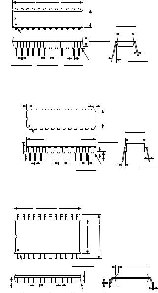
OUTLINE DIMENSIONS |
|
|
|
||||||||||
|
|
Dimensions shown in inches and (mm). |
|
|
|||||||||||
|
|
|
Plastic DIP (N-24) |
|
|
|
|
|
|||||||
|
|
1.228 (31.19) |
|
|
|
|
|
|
|
|
|
|
|
||
|
|
1.226 (31.14) |
|
|
|
|
|
|
|
|
|
|
|
||
24 |
|
|
|
|
13 |
0.260 ± 0.001 |
|
|
|
|
|
||||
|
|
|
|
|
|
|
|
|
|
|
|||||
1 |
|
|
|
|
12 |
(6.61 ± 0.03) |
|
0.32 (8.128) |
|
||||||
|
|
|
|
|
|
|
|
|
|
||||||
PIN 1 |
|
|
|
|
|
|
|
|
|
|
0.30 (7.62) |
|
|||
|
|
|
|
|
|
|
|
|
|
|
|
|
|
||
|
|
|
|
|
|
|
0.130 (3.30) |
|
|
|
|
|
|||
|
|
|
|
|
|
|
0.128 (3.25) |
|
|
|
|
|
|||
0.02 (0.5) |
|
0.11 (2.79) |
0.07 (1.78) |
|
SEATING |
|
|
|
0.011 (0.28) |
|
|||||
|
|
15 |
|
|
0.009 (0.23) |
|
|||||||||
0.016 (0.41) |
0.09 (2.28) |
0.05 (1.27) |
|
PLANE |
|
|
|||||||||
|
0 |
|
|
|
|
||||||||||
|
|
|
|
|
|
|
|
||||||||
|
|
|
|
Cerdip (Q-24) |
|
|
|
|
|
||||||
0.005 (0.13) MIN |
|
|
0.098 (2.49) MAX |
|
|
|
|
|
|||||||
24 |
|
|
|
|
|
|
13 |
|
0.310 (7.87) |
|
|
|
|||
|
|
|
|
|
|
|
|
|
|
|
|
||||
1 |
|
|
|
|
|
12 |
|
0.220 (5.59) |
|
|
|
||||
|
|
|
|
|
|
|
|
|
|
|
|
||||
|
|
PIN 1 |
|
|
|
|
|
|
|
|
|
0.320 (8.13) |
|
||
|
|
|
|
|
|
|
|
|
|
|
0.290 (7.37) |
|
|||
|
|
1.280 (32.51) MAX |
|
|
|
0.060 (1.52) |
|
||||||||
|
|
|
|
|
|
|
|
||||||||
0.200 (5.08) |
|
|
|
|
|
|
|
|
0.015 (0.38) |
|
|
|
|||
MAX |
|
|
|
|
|
|
|
|
0.150 |
|
|
|
|||
|
|
|
|
|
|
|
|
|
|
|
|
||||
0.200 (5.08) |
|
|
|
|
|
|
|
|
(3.81) |
|
|
|
|||
0.125 (3.18) |
|
|
|
|
|
|
|
|
MIN |
|
|
0.015 (0.38) |
|||
|
|
|
|
|
|
|
|
SEATING |
|
||||||
0.023 (0.58) |
0.100 (2.54) |
0.070 (1.78) |
|
||||||||||||
15° |
0.008 (0.20) |
||||||||||||||
0.014 (0.36) |
BSC |
0.030 (0.76) PLANE |
|
||||||||||||
|
0° |
|
|
||||||||||||
|
|
|
|
SOIC (R-24) |
|
|
|
|
|
||||||
|
|
0.614 (15.6) |
|
|
|
|
|
|
|
|
|
|
|
||
|
|
0.598 (15.2) |
|
|
|
|
|
|
|
|
|
|
|
||
24 |
|
|
|
|
13 |
|
|
0.419 (10.65) |
0.394 (10.00) |
|
|
|
|
|
|
1 |
|
|
|
|
12 |
0.299 (7.60) |
0.291(7.40) |
|
|
|
|
|
|||
PIN 1 |
|
|
|
|
0.1043 (2.65) |
|
|
|
0.0291 (0.74) |
45 |
|||||
|
|
|
|
|
0.0926 (2.35) |
|
|
|
0.0098 (0.25) |
||||||
|
0.050 |
0.019 (0.49) |
|
|
|
|
|
|
8 |
0.050 (1.27) |
|
||||
0.012 (0.30) |
SEATING |
|
|
|
0 |
0.015 (0.40) |
|
||||||||
0.004 (0.10) |
(1.27) |
0.014 (0.35) |
0.013 (0.32) |
|
|
|
|||||||||
PLANE |
|
|
|
||||||||||||
|
|
BSC |
|
|
|
|
|
0.009 (0.23) |
|
|
|
||||
C1933c–2.5–6/00 (rev. C) 01359
PRINTED IN U.S.A.
–14– |
REV. C |