

8.4 Chemical routes to manufacturing |
289 |
|
|
answer, these surface processes can be responsible for observed structures with lateral length scales in the 10 nm range.
8.4Chemical routes to manufacturing
Although this book, including this chapter, has been written largely from the perspective of materials physics, materials-oriented chemistry plays an enormous role in device development. Chemists are also being drawn into the ®eld of combinatorial materials discovery, a practically based mix of combinatorial chemistry and thin ®lm deposition techniques, used to search for new compounds and compositions. Such developments are discussed brie¯y in this section.
8.4.1Synthetic chemistry and manufacturing: the case of Si±Ge±C
The growth of Ge and SiGe alloys on Si(001) was considered in some detail in section 7.3.3. It is the simplest example of strained layer growth, and we described how the low mismatch alloys can be grown as layers suitable for heterostructures, or the strain can induce islands to form, which may (or may not) have potential as quantum dots. But do we want islands, or would layers be better? The answer, of course, depends on the application envisaged, but in general layers are preferable. So let's try mixing in another element, which relieves the strain and so promotes layer growth. This is the motivation behind research on the Si±Ge±C system; by mixing in the right amount of carbon one can hope to compensate for the strain introduced by Ge.
But how to do it? CVD is the most widely used manufacturing technique, starting
from silane (SiH4) and germane (GeH4), so mix in some methane (CH4) and see what happens. But some knowledge of thermochemistry is required, and this tells us that
methane is much more stable than both silane and than germane, which means that
CH4 does not want to break up. Moreover, the solubility of C in Si or Ge is very low (,131026 % in equilibrium at the Si melting point, and even lower in Ge), so the
carbon which does form is likely to be in the form of SiC, which is not what we want;
in practice up to 1±2% has been incorporated at SiGe CVD process temperatures , 700°C. Somehow we have to trick the system, thermodynamically and kinetically.
This has been done by creating custom-built molecular precursors to use as the source material.
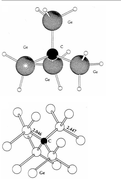
One group in Arizona (Kouvetakis et al. 1998a) has been developing compounds
with an inbuilt tetrahedral arrangement involving one C atom surrounded by four SiH3 or GeH3 ligands, as illustrated in ®gure 8.19(a). These are sizable van der Waals molecules, which are liquids at room temperature and evaporate easily. They are also reac-
tive, in that they lose hydrogen easily, and hence can incorporate the tetrahedral units
Si4C and Ge4C into a growing ®lm.
These molecules are crowded, and have bond lengths very diVerent from normal, as
indicated in the cluster calculation for GenC shown in ®gure 8.19(b). This is because the small C atom is in the middle, and the much larger Si and especially Ge atoms are
290 8 Surface processes in thin ®lm devices
(a)
(b)
Figure 8.19. (a) The precursor molecule (GeH3)3C, with Ge±C and other bond lengths determined by gas phase electron diVraction; (b) structure of substitutional C in Ge and the associated Ge±C and Ge±Ge bond lengths in a calculated (Ge)nC cluster (after Kouvetakis et al. 1998a,b, reproduced with permission).

8.4 Chemical routes to manufacturing |
291 |
|
|
competing for space around it. However, this processing route suppresses the segregation of the C atoms, because they are always surrounded by Si or Ge, and Kouvetakis et al. (1998b) have been successful in incorporating 5±6%C into ®lms grown at 470°C, which have relatively few defects (and no SiC precipitates) as seen by TEM. Starting molecules with carbon on the outside would not be nearly as eVective in this respect; in other words, by using these special molecules and relatively low processing temperatures, carbon has been tricked to remain in solution.
Whether this work represents a real breakthrough or just a very interesting development depends on the next stage ± will the clever molecules be incorporated into actual manufacturing processes or not? The role of relatively small contract research ®rms in smoothing the path to manufacturing is interesting; such processes will certainly not be incorporated into large scale Fab lines overnight. Increasingly, it is the equipment manufacturers who incorporate new processes such as this one, in order to be able to persuade the large scale producer (of e.g. computer chips) to adopt such technologies when they reinvest the next few US$ billion.3
8.4.2Chemical routes to opto-electronics and/or nano-magnetics
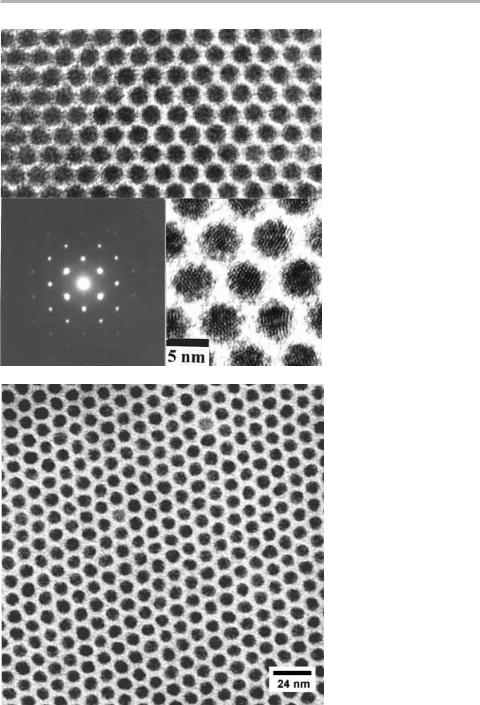
Optoelectronics, the integration of light sensitive devices with micro-electronics, is another huge ®eld in which surfaces and thin ®lms play a major role. One of the main interests in the growth of III±V and II±VI compounds is related to the ability to integrate such devices with silicon in the form of `band gap engineering' as discussed in sections 7.3.4 and 8.2.3. Quantum dots are a hot topic touched on in section 8.2.4, where the intent is that uniform size and spacing can be achieved via self-organization. But, as always in technology, one has always to bear in mind that the most eVective solution to the original challenge or problem, might come from a completely diVerent route. One such possibility is the assembly and self-organization of ordered arrays of colloidal particles prepared by more or less traditional wet chemistry methods ± a ¯ask full of goo, a drying oven and a spray-gun may be all that is needed; I exaggerate, of course, but not by much. Such techniques are not speci®c to optoelectronics; magnetic particles can just as well be prepared and arranged in remarkably uniform arrays, as shown in ®gure 8.20.
Here the idea is to prepare II±VI materials such as CdSe in solutions containing additives which adsorb on the surface of colloidal crystals in the size range 5±10 nm, thus preventing further growth. These colloids, coated with self-assembled monolayers (SAMs), form a stable dispersion in solution, which can be made to crystallize out by gentle evaporation of the lighter component in the solution (e.g. octane from octanol at 80°C). Further warming removes all but a few ML of the additives, to the extent that 3D colloidal superlattice crystals can be grown with sizes up to 50 mm (Murray et al. 1995, Heath 1995, Collier et al. 1998).
The size distribution is amazingly narrow, as shown in ®gure 8.20, and can be further controlled by manipulation of the supersaturation as a function of time during growth.
3 Financiers should note that the US billion is used here which is only 109, rather than the UK 1012.
292 8 Surface processes in thin ®lm devices
(a)
(b)
Figure 8.20. (a) 3D Optical superlattice formed from colloidal crystals of CdSe, spacing 6.5 nm, diameter 5 nm (similar to Murray et al. 1995); (b) 2D magnetic superlattice of Ag coated Co particles, spacing 13 nm, diameter 8 nm formed by colloidal techniques (after
Murray 1999, both ®gures reproduced with permission). In both these cases the 2D hexagonal lattice extends over much larger distances than can be eVectively portrayed here.
8.4 Chemical routes to manufacturing |
293 |
|
|
Other clever tricks are to cap these dots with a compatible material such as CdS having a higher refractive index or to introduce relevant dye sensitizers onto the surface of the dots. This latter technique has been a key ingredient in the color photographic processes using AgBr crystals for a long time. By the former means the con®nement of the exciton wavefunction can be increased, and so produce stronger photoluminescence, quantum yields .50% having been demonstrated (Peng et al. 1997, Schlamp et al. 1997). However, until now the overall electro-luminescent energy eYciency has been low, and the devices are not yet stable enough for production (Peng et al. 1997, Alivisatos 1998, Collier et al. 1998).
A single electron transistor which functions at T54.2 K has been demonstrated, simply by sprinkling individual colloidal dots of CdSe across the gate region of an FET (Klein et al. 1997). As a way forward, you might take this demonstration `with a pinch of salt', but it is certainly spectacular. One of the arguments in favor of these colloidal crystals is their intrinsic cheapness, yet if there is no way of getting current in or out, or if they only work at low temperature, then we have just an intriguing demonstration, not yet an innovation. Another impressive demonstration is an FET which works at room temperature, made by dropping a single carbon nanotube across the source-drain gap (Tans et al. 1998a), and the observation of associated Coulomb blockade phenomena (Tans et al. 1998b).
8.4.3Nanotubes and the future of ¯at panel TV
A further example centers around chemical routes to the production of ®eld emission sources for computer or TV screens. As discussed in section 6.2.2, various carbides and nitrides have been researched over the years, but have never really been quite stable enough to make a serious impression on the market. Yet the conventional TV tube is the last remaining example of the vacuum triode in production; is it too destined for oblivion? If ®eld emission could be made to work reliably in the planar geometry shown in ®gure 6.13(b), then maybe it could be saved!
These thoughts have gained impetus from the discovery of both multiple and singlewalled carbon nanotubes, cylindrical intermediates between planar graphite and the closed cage fullerenes (Iijima 1991, Ebbesen & Ajayan 1992, Ajayan & Ebbesen 1997, Bernholc et al. 1997). The tubes grow as long ®laments sticking out from the substrate, and emit electrons from the ends. Filaments can be produced in bundles or matrix arrays (Collins & Zettl 1997), which diVer in detail depending on the production method. Using a plasma arc discharge, Terrones et al. (1998) have produced ®laments containing a transition metal carbide particle near the end. The carbide particle catalytically converts C-containing compounds into tubes, almost as if it were knitting a sock, as shown in ®gure 8.21. Several diVerent refractory carbides have been so encapsulated, and progress to date is reviewed by Terrones et al. (1999).
Nanotubes can join up in helical (chiral) as well as cylindrical geometries, p-n junctions along the length have been demonstrated where the chirality changes, and they also can be doped, or made, with various B±N±C mixtures. The case of BN has led to some exquisitely delicate analytical microscopy, combining pictures analogous to