

3.3 Inelastic scattering techniques |
81 |
|
|
in train to try and improve analyzer performance, typically aiming to take advantage of parallel recording in either energy or angle.
There are many examples of ARUPS results in the literature; some from Au (111) and (112), Al (100) and (110) and other metals are described by Lüth; we can see that details of the band structure can be mapped out from such data, but it is quite diYcult to separate surface and bulk states from a single set of spectra. The extraction of the surface state part of the spectrum for Si(100)231 is also described by Lüth, where it is seen that the data agree best with the dimer (pairing) model of the reconstruction. Thus detailed analysis of the electronic structure can in principle provide atomic structural information. These studies of electronic structure have occupied some of the best experimentalists and theorists over a substantial period (Siegbahn et al. 1967, Cardona and Ley 1979, Himpsel 1994, Bonzel & Kleint 1995, Hüfner 1996).
3.3.3Auger electron spectroscopy: energies and atomic physics
In this and the following two sections, Auger electron spectroscopy (AES), its use as a quantitative analysis tool, and on a microscopic scale, is treated in more detail. The Auger process was discovered by Pierre Auger in 1925±26, when he observed tracks of constant length in a cloud chamber, and thereby inferred that the particles had constant energy; however, the technique was not used to study surfaces until the late 1950s and 1960s. Auger electron energies are closely related to the corresponding X-ray energy, and most usually are described in X-ray notation. For example, ®gure 3.11
shows the level scheme associated with the Si KL1L2,3 transition, one of a set of KLL transitions, the strongest of which is experimentally observed at ,1620 eV. The ®nal
state contains two holes in the K shell; the Auger process is a competing way to ®ll the initial core hole, and so is an alternative to Si K X-ray emission.
These Auger energies have historically been given by approximate formulae, e.g. by Chung & Jenkins (1970):
E(KL1L2)5EK(Z)2 0.5 {EL1(Z)1EL2(Z)}2 0.5{EL1(Z1D)1EL2(Z1D)}, (3.4)
where the use of the average energy is due to being unable to distinguish which electron ®lled the core hole. The D has been used to indicate that the ®nal emission is from an ion, not a neutral atom, which shifts the ®nal energies downwards slightly. For practical surface analysis, one needs to know that these energies are known, and are typically displayed on a chart in every surface science laboratory. The energy measured does, however, depend on whether you are measuring in the dN(E)/dE or N9 mode, where the negative-going peak is typically quoted, or in the N(E), or E´N(E) mode, where the positive-going peak is quoted (see ®gure 3.8). These can be separated by several electronvolts; the width of the Auger peak is typically 1±2 eV, due to a rather short lifetime before Auger emission. The Auger peak width can be further broadened by overlapping peaks, by wide valence bands, or by analyzers which are set to increase sensitivity at the expense of resolution. In addition, to quote the absolute energy relative to the vacuum level of the element, a negative correction to (3.4) equal to the work function of the analyzer (4.5 eV typically) is needed (McGilp & Weightman 1976);

82 3 Electron-based techniques
Auger |
Energy loss |
||
electron |
electrons |
||
|
Vacuum level |
||
0 eV |
EC |
Density |
|
EF |
|||
of states |
|||
|
|||
|
V |
V1 |
|
|
|
||
~13 |
|
V2 |
|
99 |
L2,3 |
Primary |
|
electron |
|||
|
|
||
149 |
L1 |
creates a |
|
core hole |
|||
|
|
||
1839  K
K
Figure 3.11. Si KLL Auger scheme, after Chang (1974). See text for discussion.
however, if one quotes energies relative to the Fermi level, this correction to (3.4) is not required (Seah & Gilmore 1996).
The theory of Auger emission is rooted in atomic physics, and is only modi®ed slightly by solid state and surface eVects. Thus the calculation needs to take into account whether the atom in question is L±S or j±j coupled, illustrated for the KLL series in ®gure 3.12. As atomic calculations have improved, formulae which explicitly acknowledge the energy relaxation due to the ®nal state ion, and the spectroscopic con- ®guration of the two holes have been developed (Shirley 1973, Weightman 1982); for example the main KLL transition in silicon has a 1D2 ®nal state. Si KLL is a primarily a case of L±S coupling, since the atomic number is small, whereas Ge KLL is in the intermediate coupling regime. A high energy resolution spectrum shows these eVects, as for Ge LMM in ®gure 3.13 and for Si KLL and Ag MNN later in ®gure 3.25. What one can see in the spectrum depends on both energy resolution and signal to noise ratio, and if X-ray excitation is used, the secondary electron background can be much reduced over electron excitation. So the peak to background ratio, while very useful for analysis as we shall see later, does depend on the analyzer settings, the mode of excitation, and the excitation energy.
The other point which is clear from the atomic physics is that X-ray and Auger emission are alternatives: either/or, not both. For low energy transitions, Auger emission is strongly favored. The Auger eYciency g512 Ã, where the X-ray ¯uorescence yield à is shown in ®gure 3.14, taken from Burhop (1952). It is noticeable that this work was done a long time ago in the context of atomic, not surface physics. Figure 3.14 shows that the proportion of K-shell Auger emission is greater than 0.5 up to about Z530 (zinc). So, typically, one switches which transition is used as we move up the periodic table: KLL transitions for light elements, LMM after that, and then MNN.
3.3 Inelastic scattering techniques |
83 |
|
|
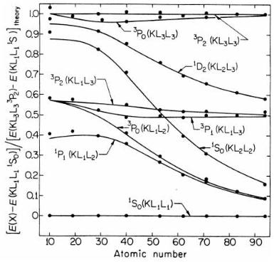
Figure 3.12. Reduced KLL Auger energy diVerences as a function of atomic number, corresponding to the transition form L±S coupling at low atomic number to j±j coupling at high atomic number. The nine components are labelled on the plot, with theoretical curves as full lines and points from experiment (after Shirley 1973, reproduced with permission).
The Auger eVect is due to the Coulomb interaction between the core hole and the ejected electron which leaves the other hole behind. The transition rate for this process was solved very early in the history of quantum mechanics by Wentzel in 1927, who calculated transition matrix elements (Fermi's golden rule) between the initial (atomic) and the ®nal (continuum) states. This is set out in detail for both relativisitic and non-relativistic cases by Chattarji (1976). One can use simple arguments which bring out what is basically going on as follows. The Auger transition rate,
b |
5(2p/")|Kx c |
|e2/|(r |
2 r |
)||x |
c |
L|2, |
(3.5) |
n |
f f |
1 |
2 |
i |
i |
|
|
where the wavefunctions cf5emitted electron (continuum) and xf5electron in the lower band. On the other hand, the X-ray ¯uorescence yield is the one-electron dipole matrix element, namely
a |
5(2p/")k|Kx |er |x |
L|2, |
(3.6) |
|
n |
f |
i |
|
|
where the constant k54/3 (v/c)3, with the radiation frequency v/2p given by "v5 EK 2 EL. Now if we assume Bohr-like atoms EK ,2Ze2/r and r,a0/Z, with the
84 3 Electron-based techniques
Figure 3.13. High resolution AES spectrum of Ge LMM for 5 keV incident energy (after Seah & Gilmore 1996, reproduced with permission). The strongest peaks, within the L2 M4,5M4,5 series at 1145 and L3 M4,5M4,5 series at 1180 eV have 1G4 symmetry; the smaller peaks at higher E consist of three overlapping lines with 3F symmetry (McGilp & Weightman 1976, 1978).
Bohr radius a05"2/(me2), we can deduce that vK ,Z2, and v3r2 ~Z4. So the X-ray ¯uorescence yield
Ã5oa |
/(oa |
1ob |
)51/(11a |
Z24), |
(3.7) |
n |
n |
n |
K |
|
|
where aK is a constant for K-shell emission, as shown in ®gure 3.14. To recap: these models all depend on atomic and ionic wavefunctions for energies, transition rates, ¯uorescence yields, and are not speci®c to solids or surfaces. Note that several books on surface analysis pitch straight into the technical details without mentioning any of this at all; but atomic physics lies behind many of the ®ner eVects.
3.3.4AES, XPS and UPS in solids and at surfaces
The state of matter aVects the lineshape, and causes energy shifts. If the transitions
involve the valence band, then we refer to LVV etc, or more generally to core±valence± valence (CVV) transitions. For example, Si LVV has a transition at ,90 eV; these tran-
sitions are sensitive to chemical state, as shown in ®gure 3.15, and Al LVV has a diVerent lineshape in metallic Al and in aluminum oxide (®gure 3.10(c)). Many authors have studied core level shifts in UPS and XPS. An account of this history in the context of semiconductor surfaces is given by Himpsel (1994); the use of spectral shapes as `®n- gerprints' of particular chemisorbed states is discussed by Menzel (1994).

3.3 Inelastic scattering techniques |
85 |
|
|
K
Fluorescence ϖyield
0.9
0.8
0.7
0.6
0.5
0.4
0.3
0.2
0.1
0.0 |
10 |
20 |
30 |
40 |
50 |
60 |
70 |
80 |
90 |
0 |
Z
Figure 3.14. Fluorescence yield ÃK for K-shell X-rays compared with non-relativistic (full line) and relativistic (dashed line) models, compared with experimental data measured between 1926 and 1950 (after Burhop 1952, reproduced with permission).
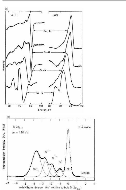
The precise shape of an Auger or photoelectron line is an ongoing topic which is researched in a few specialist groups worldwide. In the simplest case, the UPS spectrum gives this density of states directly, and the lineshape of LVV Auger transitions re¯ects a self-convolution of the valence band density of states. Both of these shapes are diVerent in a compound containing the element, from that in the element itself. Early Auger spectra for Si in diVerent chemical environments are compared with optimized UPS spectra in individual oxidation states at the Si±silicon dioxide interface in ®gure 3.15 (Madden 1981, Himpsel et al. 1988, Himpsel 1994). The shift to lower energies in the compounds is apparent from these ®gures.
For both UPS and AES, many-body ®nal state eVects can cause signi®cant changes in the lineshape, if the valence hole in the ®nal state feels the eVect of the core hole in the initial state. This depends on the energy cost of localizing two holes on the same
86 3 Electron-based techniques
Figure 3.15. (a) Si Auger spectra in various environments (after Madden 1981); (b) Si plus thin oxide, as observed in synchrotron radiation UPS by Himpsel et al. (1988), showing a shift to lower energies with increasing oxidation state (both diagrams reproduced with permission).
3.3 Inelastic scattering techniques |
87 |
|
|
Figure 3.16. (a) Calculated Auger emission spectrum as a function of U/W for a CVV Ni spectra; (b) comparison of Ni L3VV in Ni and in La3Ni with Cu L3VV Auger spectra, including calculated (full and dashed) lines based on appropriate values of U for the diVerent atomic states (after Bennett et al. 1983, reproduced with permission).
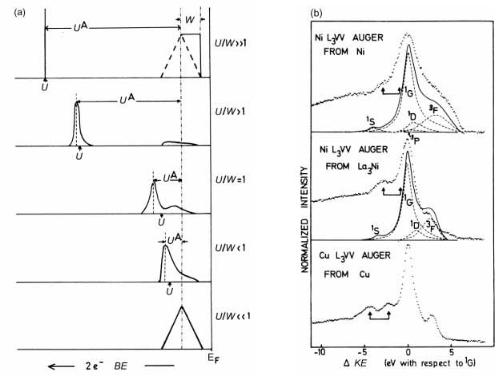
atom (the correlation energy U, often associated with the `Hubbard' model), versus the valence band width, W (Verdozzi & Cini 1995). If U/W is ,,1, we see an unshifted self convolution (self fold) of the valence band, corresponding to a delocalized, band-like ®nal state; in the other limit (W/U ,,1) we see a shifted, but atomic-like, line. The Auger CVV transitions then show multiplet structure where the details depend on the variation of the matrix elements with the orbital character of the ®nal state.
As a result of these considerations the lineshape can switch from one type to the other across a series of alloys. This eVect happens particularly for nearly ®lled d-shells, as in Pd or Ni alloys and silicides. A schematic diagram of this eVect plus an example of Ni LVV in Ni-based alloys (Fuggle et al. 1982, Bennett et al. 1983) is shown in ®gure 3.16, but there is ongoing discussion about how such models apply to un®lled bands, where many diVerent possibilities for screening exist. This type of work is reviewed by Weightman (1982, 1995) and Hüfner (1996), and is becoming more important as the ®ner aspects of electron spectroscopy, including spin-polarized electron spectroscopy of magnetic materials as discussed in chapter 6, can be interpreted in terms of the electronic structure.
All these electron spectroscopies derive their surface sensitivity from the low inelastic mean free path (imfp) of electrons, which has a minimum in the neighborhood of

883 Electron-based techniques
50±100 eV, and a typical minimum value of around 0.5 nm. Calculating the imfp has become a major activity in its own right (Powell 1994, Powell et al. 1994), but it is only in special cases that it can be readily obtained experimentally. One case which is soluble is when a deposit grows in the layer by layer mode. We consider this in connection with AES quanti®cation in the next section; other techniques are not considered here, but the approaches and problems are all very similar.
The general form of l(E) has been given as l (in ML)5538/E210.41 (aE)1/2, where a is the ML thickness in nm (Seah & Dench 1979). This formula, widely used in the 1980s for want of a better alternative, shows a minimum at about 50eV, but the form used is not rigorous; if you are doing detailed work you will need a more accurate expression, such as that given by Tanuma et al. (1991, 1993). The underlying physics is
that at high E, we have the Bethe loss law for inelastic electron scattering, which shows that (2 dE/dx),E21ln(E/I), with I equal to the mean ionization energy ,10±15 eV.
l(E) increases as E/ln(E/I), approximated by E1/2 in the Seah & Dench formula, since l is ,(dE/dx)21. At lower energy l(E) goes up strongly as E decreases, because of the
lack of states into which the electron can be scattered. For example, if the main scattering mechanism is creation of plasmons with an energy of ,15 eV, then if the energy
is within 15 eV of the Fermi level, the scattering cannot occur because the ®nal state is already occupied. This then becomes a phase space limitation at low E, which has an E22 dependence.
3.4Quanti®cation of Auger spectra
3.4.1General equation describing quanti®cation
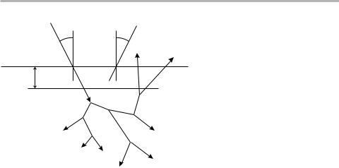
The general equation governing the Auger electron current, IA caused by a probe current Ip can be written down straightforwardly, but is not immediately transparent, and really needs to be explained using a schematic drawing, such as ®gure 3.17. The
incoming electron causes an electron cascade below the surface, whose spatial extent is typically much greater than the imfp. For example, the spatial extent is about 0.5 mm
at an incident energy E0520 keV, but also depends on the material and the angle of incidence, u0. As a result Auger electrons can be produced by the incoming primary electron beam, and also by the backscattered electrons as they emerge from the sample;
the Auger signal intensity thus contains the backscattering factor, R, which is a func-
tion of the sample material, E0 and u0.
The ratio IA/Ip can be expressed as a product of terms describing the production and detection of the Auger electrons, as ®rst developed by Bishop & Rivière (1969). The
Auger yield Y is the number of Auger electrons emitted into the total solid angle (V 5 4p sterad). It is therefore not dependent on the details of the analyzer. The detec-
tion eYciency D of the analyzer can be written as (T´«), where T is a function f(Va/4p), Va being the solid angle collected by the analyzer, and « is f(DE/E), most simply « 5 (DE/E). Thus
3.4 Quanti®cation of Auger spectra |
89 |
|
Primary θ0 |
θa Auger electron |
|
electron |
|
|
beam |
|
|
Auger |
Backscattered |
|
escape |
|
|
electrons |
|
|
depth |
|
|
|
|
|
|
Electron |
|
|
cascade |
|
Figure 3.17. Schematic diagram of electron scattering in a solid, indicating the incident and detected angles, u0 and ua, plus the role of backscattered electrons in determining the Auger signal strength. The escape depth is qualitatively the thickness of the region from which most of the detected Auger electrons originate, of the same order as the imfp discussed in the text.
IA/Ip5Y´D5[sgR]´secu0´Ne(T´«). |
(3.8) |
Here we have Y expressed as the cross section for the initial ionization event (s), the Auger eYciency (g), discussed in outline in section 3.3, and the factor R. The secu0 term describes the extra ionization path length caused by having the primary beam at an angle to the sample normal. Finally Ne is the eVective number of atoms/unit area contributing to the (particular) Auger process.
What we actually want to know is: given a measured signal IA, how many A-atoms are there on the surface? Typically there is not a unique answer to such a simple question, because the signal depends not only on the number of atoms but also on their distribution in depth. There are two cases which can be solved uniquely, which are instructive in showing how such analyses work. The ®rst is when all the atoms are in the surface layer: then Ne5N1, and if one knew all the other terms in the equation, we could determine N1.
The second case is when the atoms are uniformly distributed in depth: in this case we can show that Ne5lNm, where Nm is the bulk (3D) density of A-atoms. The proof of the second case is as follows. We work out
(Ne´T)5(1/4p)eeeN(z) exp(2 z/lcosua)´sinuaduadfadz, |
(3.9) |
where the integral is over the two analyzer angles (ua,fa) and depth z. The path length in the sample in the direction of the analyzer is z/cosua, so we are assuming exponential attenuation without change of direction; this is reasonable for inelastic scattering of the outgoing electrons. Because N(z)5Nm is constant, we can do the integration over z ®rst. This gives
90 3 Electron-based techniques
Normalised signal (20 keV)
1.8
1.6
1.4
1.2
1.0
0.8
0.6
0.4
0.2
0.0
0
(a) |
Silicon 1610 eV θ0 = 65° |
|
|
|
|
(b) |
Copper 914 eV θ0 = 65° |
|
|
||||
|
|
|
|
|
|
|
|
|
|
|
|
||
|
|
|
|
|
|
|
3.0 |
|
|
|
|
|
|
|
|
|
Harwell MA500 |
|
|
|
2.5 |
|
|
|
Harwell MA500 |
|
|
|
|
|
Sussex HB50 |
|
|
|
|
|
|
|
Sussex HB50 |
|
|
|
|
|
|
|
|
|
|
|
|
Ichimuras results |
|
|
|
|
|
|
|
|
|
|
|
|
|
|
|
|
|
|
|
|
|
|
|
ekV |
|
|
|
|
(θ0 = 45°) |
|
|
|
|
|
|
|
|
2.0 |
|
|
|
|
|
|
|
|
|
|
|
|
|
to20 |
|
|
|
|
|
|
|
|
|
|
|
|
|
|
|
|
|
|
|
|
|
|
|
|
|
|
|
normalisedSignal |
1.5 |
|
|
|
|
|
|
|
|
|
|
|
|
|
|
|
|
|
|
|
|
|
|
|
|
|
|
|
1.0 |
|
|
|
|
|
|
|
|
|
|
|
|
|
|
|
Calculations |
|
|
|
|
|
|
|
|
|
|
|
|
|
|
Worthington±Tomlin |
|
|
|
|
|
|
|
|
|
|
0.5 |
|
|
Powell |
|
|
|
|
|
|
|
|
|
|
|
|
Gryzinski |
|
|
||
|
|
|
|
|
|
|
|
|
|
|
|
||
|
|
|
|
|
|
|
|
|
|
Lotz |
|
|
|
|
|
|
|
|
|
|
|
|
|
Hartree±Fock |
|
|
|
|
|
|
|
|
|
|
0.0 |
|
|
|
|
|
|
5 |
10 |
15 |
20 |
25 |
30 |
|
0 |
5 |
10 |
15 |
20 |
25 |
30 |
|
Primary beam energy E 0 (keV) |
|
|
|
|
|
Primary beam energy E 0 (keV) |
|
|
||||
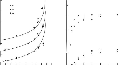
Figure 3.18. Auger peak heights for (a) Si KLL and (b) Cu L3MM as a function of primary energy E0, normalized to 20 keV, measured on Auger microprobe instruments at Harwell and Sussex, compared to the product (sR) calculated with the cross sections indicated (after Batchelor et al. 1989, reproduced withpermission).
(Ne´T)5lNm ´(1/4p)ee cosua´sinuaduadfa5lNm´f(ua, fa). |
(3.10) |
The angular double integral is just the cosine electron emission distribution, integrated over the solid angle of the analyzer; so f5T, Ne5lNm, as required.
A detailed experimental and computational study of the Auger signals from bulk elements has been performed, amongst others, by Batchelor et al. (1988, 1989). These studies show that the dependence of the Auger peak height on primary beam energy E0 explores the variation of (sR) as shown in ®gure 3.18 for Si KLL and Cu L3MM; the variation with u0 is determined by (Rsecu0´T). The dependence on atomic number Z is complicated, since all the above material variables and the Auger energy are properties of the individual element in question.
To make these comparisons we took a particular ionization cross section, and calculated the Auger backscattering factor R511r with this cross section, where r is
de®ned as |
|
r5(1/s(E0) secu0)ee s(E)(d2h/dEdu)sinududE, |
(3.11) |
where the normal electron backscattering factor h is given by |
|
h5ee (d2h/dEdu)sinududE. |
(3.12) |
3.4 Quanti®cation of Auger spectra |
91 |
|
|
Signal normalized to 45°
Harwell MA500
(a)
4.0
Silicon
Copper
3.0
Tungsten
2.0
1.0
0.0
0.0
0.0 |
0 |
10 |
20 |
30 |
40 |
50 |
60 |
70 |
80 |
90 |
±10 |
Tilt angle (deg)
Peak to background ratio
Harwell MA500
(b)
Incident angle, θ0
 65°
65°
2.5

 75°
75°
Silver 345 eV
2.0
1.5
1.0
Tungsten 1730 eV
0.5
0.0 |
5 |
10 |
15 |
20 |
25 |
30 |
0 |
Primary beam energy E0 (kV)
Figure 3.19. Variation of Auger peak to background ratio for (a) Si, Cu and W with incidence angle u0, compared with model calculation based on (3.13); (b) Si and Cu with primary beam energy E0 at two incidence angles u0565 and 75° (after Batchelor et al. 1989, reproduced with permission).
This means that the Auger backscattering factor can be written as R511bh, where the factor b is typically greater than 1, and depends on the energy and angular distribution of backscattered electrons, and the Auger energy in relation to the beam energy. Comparison of the energy dependences of the cross sections and other checks on absolute values has advanced knowledge of which cross sections are reliable (Batchelor et al. 1988, Seah & Gilmore 1996).
The peak to background ratio (P/B or PBR) can be measured accurately and is very useful as an approximate compensation for topographic eVects. The angular dependence is rather ¯at as shown in ®gure 3.19(a) for Cu, Si and W Auger electrons measured in two diVerent instruments. The lines are a simple model calculation based on
P/B ~ sec(u0)R(u0)/h(u0), |
(3.13) |
and it is seen that this model, normalized at normal incidence, gives a good ®t out to at least u0570°. At high incidence angle, there is much less variation in the back scattering factor as a function of atomic number, and the background becomes dominated by secondary electrons, which have similar excitation mechanisms to Auger electrons. This is mirrored in the PBR as a function of E0, shown in ®gure 3.19(b). Above 15±20 keV both Cu L3MM and Si KLL show no dependence on E0; this eVect sets in at lower E0 for lower energy transitions, where the background comprises secondary rather than backscattered electrons (Batchelor et al. 1989).