

8.3 Conduction processes in thin ®lm devices |
281 |
|
|
8.3.1Conductivity, resistivity and the relaxation time
All electrical properties of thin ®lm devices depend essentially on the number of charge carriers and the scattering processes to which these charges are subjected. To study such topics we need access to a book describing conduction processes in the relevant type of material. For normal metals and alloys, Rossiter (1987) is excellent; however, this book does not discuss superconductors or semiconductors even in outline. The reason is simply that these three topics are enormous ®elds, each with its own appropriate starting point. For superconductors, much eVort has to be expended to describe the thermodynamic and quantum mechanical nature of the superconducting state, before one can consider the eVects of bulk scattering and then thin ®lm and surface eVects (Tinkham 1996). The fabrication of useful high-Tc ceramic wires and tapes is a major technical challenge.
In particular, we can note that in semiconductors, most attention is paid to the number and type of carriers, and then we consider scattering processes which determine carrier mobility. For example, we write the conductivity s as
s5q(nme or pmh), |
(8.10a) |
in terms of the electron or hole mobilities me and mh, given by |
|
m5qt/m*, |
(8.10b) |
where both the densities, n or p, and the scattering processes which lead to the eVective scattering time t, are determined by the defect density. Note that the word or is used here in the same sense as in section 8.1.2, to avoid too detailed a discussion of what happens if both n- and p-type dopants are present simultaneously, when extra care is always required. The eVective mass is inversely proportional to the band curvature, and is in general a tensor quantity.
In metals, the number of carriers is essentially ®xed, and the spotlight is on scattering processes. Elementary considerations start with the Drude model, and show that the conductivity is proportional to the density n of conduction electrons and the relaxation, or scattering, time t between collisions as in equations (8.10) and (8.11). Moving to the quantum model with the correct Fermi±Dirac distribution function fk, we realize that only those electrons n(k) close to the Fermi energy participate in the scattering, and that the scattering time is now quite a complex average of all scattering processes. In the regime where the linearized Boltzmann transport equation (Rossiter 1987, chapter 1) is appropriate and we consider only elastic scattering,
tk215(2p)23edk9Qkk9(12 fk9), |
(8.11) |
where Qkk9 is the matrix element for scattering processes from k to k9 which conserve energy.
In general, the conductivity, relating the current density J to the electric ®eld E is a second rank tensor Ji5sijEj and the conductivity can be expressed as an integral over the Fermi surface S as
s |
ij |
5{e2/(2p2h)}e t v |
(k)v |
(k)dS/ |v(k)|, |
(8.12a) |
|
k i |
j |
|
|

282 8 Surface processes in thin ®lm devices
where v(k) is the Fermi velocity. For a cubic or amorphous metal, where the relaxation time is a function of the magnitude of k, but not of direction, (8.12a) simpli®es to
s5{e2/(6p2h)}e t v(k)dS, |
(8.12b) |
k |
|
so that s and r are both scalar quantities and s5r21. But, even so, we note that if a new scattering mechanism is added in (8.12), this will contribute to tk21, where the shortest time will dominate, but that the contribution to s (in (8.12) as in (8.10)) is proportional to tk. Thus the contribution of a new scattering process to the resistivity r is as an inverse of an inverse.
8.3.2Scattering at surfaces and interfaces in nanostructures
Given that many materials in general, and surface scattering in particular, are not intrinsically isotropic, the contribution of surface or 2D interface processes to the resis- tivity can be quite complicated. The ®rst model applicable to thin ®lms, which assumed an isotropic Fermi surface, was summarized by Sondheimer (1952) in terms of a single parameter p which characterized whether the scattering at the surface was specular (p 51) versus diVuse (p50). DiVerent formulae are applicable to wires or grain boundaries (Sambles & Preist 1982, Rossiter 1987 chapter 5), but for the thin ®lm case, the Fuchs±Sondheimer formula is
|
3(1 2 r) |
` |
|
1 2 exp( 2 kt) |
||
r`/r512 3 |
|
|
E(t23 |
2 t25) 1 |
|
2 dt4, |
2k |
1 2 p exp( 2 kt) |
|||||
|
|
|
1 |
|
|
|
(8.13)
where k is d/L`, and t is the integration variable corresponding to the direction of electron travel. This formula clearly shows that as p→1 there is no extra scattering due to the surface, but if the scattering has a diVuse component, then the resistivity ratio r/r` rises rapidly as the ®lm thickness d becomes less than the scattering mean free path L` in the corresponding bulk material, i.e. as k →0. This formula is not the most accurate, but it is the simplest which has analytic limits.
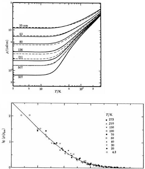
The earliest comparisons with experiment typically showed agreement with (8.13) with p close to zero, the diVuse scattering limit. However, these early experiments were largely limited to thin polycrystalline ®lms in which grain-boundary scattering played a crucial role. In several experiments, Al ®lms were used which has a rough oxide on the surface. A particularly careful study of the resistivity of Au ®lms grown on mica and KBr was made by Sambles et al. (1982), as illustrated in ®gure 8.16. Here Au(111) samples of diVerent thicknesses were grown on mica, and the resistivity measured as a function of temperature. We can see in ®gure 8.16(a) that at low temperatures there is a substantial residual resistivity which increases with decreasing ®lm thickness. The same data plotted on a logarithmic scale of r` /r versus k shown in ®gure 8.16(b) gives a good ®t to the more detailed model of SoVer (1967), but the ®t may not be uniquely due to surface scattering. Internal surfaces such as grain boundaries can mimic surface scattering if the grain size is larger in thicker ®lms (Sambles 1983). He concluded that `p' in such ®lms can be as high as 0.65, and that grain and twin boundary scattering
8.3 Conduction processes in thin ®lm devices |
283 |
|
|
(a)
(b)
Figure 8.16. (a) Temperature dependence of the resistivity of Au(111) ®lms of diVerent thicknesses grown on mica, showing strongly thickness dependent residual resistivity; (b) the same data on a log±log plot of r/r` versus k5d/L` (after Sambles et al. 1982, reproduced with permission).
can also be strong. Thus from here on we consider both internal interfaces and external surfaces as sources of scattering.
Electron transport in semiconductor structures with dimensions down to a few nanometers have many interesting (and sometimes disturbing) properties for future devices. There is a limit due to the statistical distribution of donors, acceptors and scattering centers. A simple calculation shows that a device based on 1018 cm23 donors or
2848 Surface processes in thin ®lm devices
acceptors, a relatively high doping level, will have only one impurity somewhere in the
width of a 10 nm square wire. Chaotic eVects are expected once the number of electrons/ impurities drop to below ,10 per device cross section, so the size region ,30 nm is considered very dubious. We are not there yet: the next generation of 0.13 mm (130 nm) linewidth devices is in the pipeline, but it is not too soon to start worrying about these topics.
Second, the size eVect on electronic energy levels, as illustrated in ®gure 8.14 for quantum well structures, means that via electron±electron interactions, energy levels in the device depend on the occupation numbers of the diVerent electron energy levels. This is of course the same as in individual atoms and molecules, but in the case of
.10 nm sized devices, the energy levels are much closer together. Thus at suitably low temperatures, conduction processes through these devices will be aVected by the eVects known collectively as the Coulomb blockade. This is a rich ®eld for theoretical research and experiments at low temperature and high magnetic ®elds (Ferry & Goodnick 1997), and is the origin of collective aspects of electronic behavior behind the fractional quantum Hall eVect and the 1998 Nobel prize for Physics awarded to Luttinger, Störmer and Tsui (Mellor & Benedict 1998, Schwarzschild 1998).
But before we all get carried away, we should note that the reason these subtleties can be observed at all is due to the low temperature and high magnetic ®elds which allow the closely spaced energy levels to be separated. As Störmer himself noted on the award of the prize `No, it won't revolutionize telecommunications' (Schwarzschild 1998). Devices which operate at room temperature (or even 77 K) need to be more robust in this sense. But many groups are involved in the race to demonstrate single electron transistors (SETs) which work at room temperature. The active regions of such devices must have a characteristic dimension ,10 nm (Devoret & Glattli 1998). This is the principal reason for believing that if even smaller devices are to become important in future, then the carrier density needs to be higher than in typical semiconductors. For example, such devices are increasingly sensitive to random radiation eVects as the number of carriers is reduced. Interest is therefore turning to metallic systems, and in particular to magnetic eVects which can be used in non-volatile devices; some of these are described in the next section.
8.3.3Spin dependent scattering and magnetic multilayer devices
The giant magneto-resistance (GMR) eVect is the reduction of (longitudinal) resistance in the presence of a (parallel) magnetic ®eld, typically in a magnetic multilayer. In a large ®eld, where the magnetization in all the layers are lined up, the `spin-¯ip' scattering of the conduction electrons is minimized, whereas when some of the layers are aligned antiparallel it is greater. The biggest eVects observed are changes of up to 80% of the resistance at high ®elds at low temperatures. Note that the sign of the magnetoresistance in ferromagnetic materials, decreasing as the ®eld is increased, is opposite to that in normal metals, where the helical paths followed by electrons in an external ®eld yield more opportunities for scattering. This distinction is spelled out in an in¯uential report (Falicov et al. 1990), which was largely responsible for setting the agenda for

8.3 Conduction processes in thin ®lm devices |
285 |
|
|
research on magnetic materials and thin ®lm devices during the 1990s. The push is now on to integrate magnetic superlattices with semiconductors, with the goal of high density non-volatile memory a realistic prospect in the not too distant future (DeBoeck
&Borghs 1999, Daughton et al. 1999).
In magnetic materials we have to consider that there are two resistivity channels2, r↑
and r↓. At low temperatures in ferromagnetic materials, spin-¯ip scattering is frozen out, meaning that the spin-up and spin-down channels behave independently and that conductivities add as s5s↑1s↓, or equivalently r215(r↑)211(r↓)21. Within each resistivity channel, we have the diVerent scattering mechanisms contributing in proportion to inverse relaxation times as discussed in section 8.3.1, and at ®nite temperatures magnon scattering, which tends to equalize the contributions of the two spin channels, is also possible. Thus it is not surprising that this topic can get quite complicated quite quickly; a useful introduction in the context of magnetic multilayer devices, where spin dependent scattering at interfaces is the most important eVect, is given by Fert & Bruno (1994). Spin dependent scattering of the same type has also been demonstrated at aligned domain walls in pure Co and Ni ®lms (Gregg et al. 1996).
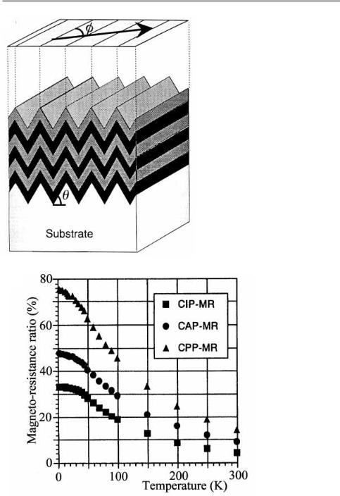
Multilayer devices can be constructed in various diVerent geometries, limiting cases being when the current is either in the plane (CIP) or perpendicular to the plane (CPP). The way in which one of the two resistivity channels can short circuit the other depends on the device geometry. For a sizable device, the CIP geometry tends to have the higher resistance, but the boundaries between the layers are less eVective in producing spin ¯ips than in the CPP geometry, which has higher resistivity. But the low resistance of the conventional CPP geometry means that the eVects due to the thin device are very diYcult to measure, because all the other resistances add in series. This CPP problem has lead some workers to go to considerable lengths to create structures in the CAP geometry, with the current at an angle to the plane, which can be done by using ridged substrates at an angle u, is illustrated in ®gure 8.17(a).
The conductivity in the CAP geometry combines those of the other geometries as
s |
CAP |
5s cos2u1s |
CPP |
sin2u, |
(8.14) |
|
CIP |
|
|
and there are similar formulae for the combination magneto-resistance (Levy et al. 1995). Ono & Shinjo (1995) and Ono et al. (1997) have used Si(001) wafers, and have etched V-grooves with {111} facets into this substrate, on which the multilayers are grown. By varying the angle of the current direction f, they could measure sCAP and sCIP on the same samples, and use interpolation formulae to estimate sCPP. The results of a particular sample are shown in ®gure 8.17(b); this corresponds to a 4 mm thick, 91-layer stack of four individual layers with composition Co(1.2)/Cu(11.6)/NiFe(1.2)/ Cu(11.6), where the layer thickness in nm is given in brackets. Note that the MR ratio for this system in the CAP geometry reaches almost 50% at low temperature and is around 10% at room temperature. Although one could use higher values, these are
2This notation allows one to write an article entitled The art of sp↑n electron↓cs (Gregg et al. 1997), but the large number of authors on this paper suggests that they know they could only do this once and get away with it.
286 8 Surface processes in thin ®lm devices
(a)
(b)
Figure 8.17. (a) Schematic illustration of a multilayer constructed on a substrate containing V-grooves at characteristic angle u, with the current ¯owing in a direction given by the angle f;
(b) the measured magneto-resistance observed as a function of temperature in the CIP and CAP geometries, and the estimated CPP results, for a composite multilayer of Co/Cu/NiFe/Cu as described in the text (from Shinjo & Ono 1996, reproduced with permission).
8.3 Conduction processes in thin ®lm devices |
287 |
|
|
good enough for magnetic ®eld sensors, and read/record heads using GMR multilayers are already commercially available.
In the above example, the nonmagnetic spacer layers (of Cu) were suYciently thick to ensure that the magnetism of the Co and NiFe layers are not coupled directly via the conduction electrons. This is in contrast to the much thinner spacer layers discussed in section 6.3.4 and illustrated in ®gure 6.24. At intermediate thicknesses, this spindependent coupling leads to complex magnetization curves, and the transfer of spin `information' from one part of a device to another, which can be used in spin valves or spin transistors (Parkin et al. 1991, Johnson 1993, 1996, Parkin 1994, Monsma et al. 1995). The next stage may be to make use of spin polarized currents induced by magnetic elements into the substrate itself, and then to use these currents as the injector for a hot electron device (Gregg et al. 1996). The acronym for this UK-based development, SPICE (spin polarized injection current emitter), may have something to do with the existence of a popular all-female vocal group of the same name at around the same time. We shall see what becomes of both.
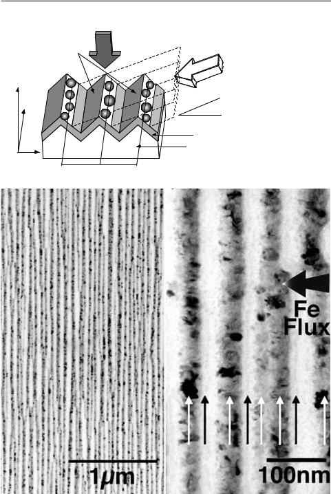
Another possible way forward, not involving magnetic coupling through the substrate, is to use magnetic wires grown on insulators; these wires have anisotropic magnetic properties, as well as being a more favorable geometry for CPP GMR measurements. NaCl(110) is a substrate with a high surface energy, and self-organizes into facets on (001) planes at 45° to the substrate plane. By deposition at a shallow angle, narrow wires will be produced at the tops of the ridges shown in ®gure 8.18(a), and these wires can then be capped to prevent oxidation, etc. In a series of experiments, Sugawara et al. (1997) ®rst deposited a thin SiO layer on either NaCl(110) or (111), followed by Fe deposition at a shallow angle, followed by a further SiO layer.
This procedure allowed them to produce isolated islands aligned in one dimension, continuous parallel wires, or isolated Fe dots of various sizes. They could then remove the SiO/Fe/SiO assembly by dissolution of the substrate for TEM examination, and to make particle and wire density observations, exactly as described here in section 5.3, as shown in ®gure 8.18(b). The new feature is of course the ability to perform magnetic and magneto-optical (Kerr) measurements before this stage, similar to that shown here in ®gure 6.18, and hence explore magnetic anisotropy, dipole couplings and the paramagnetic to ferromagnetic transition as a function of particle size (Sugawara & Scheinfein 1997). There are a large range of parameters to explore, just within this one system, if anyone wants to take these results to the next stage of implementation as a working device.
Another system which clearly shows promise as a magneto-optical device is based on the nucleation of Co dots on Au(111), at the position of the surface vacancies which occur at the intersection of the (2331) herringbone reconstruction, ®rst observed by Voigtländer et al. (1991) and described here in section 5.5.3. A strong Kerr eVect signal from ML deposits in these dots has been observed by Takashita et al. (1996), and Fruchart et al. (1999) have constructed well ordered Co pillars in Co/Au (111) multilayers, with improved magnetic properties. Whether or not this system will end up in a real device is not clear: are we ready to use surface reconstructions and surface point defects so directly in a manufacturing process? Whatever the
288 8 Surface processes in thin ®lm devices
(a) |
SiO deposition |
[110]
[001]
(010) |
(100) |
|
[110]
Fe dots
Fe flux
20ë
a-SiO
NaCl (110) substrate
(b) |
|
(c) |
Figure 8.18. (a) Shadow deposition at glancing angle onto ridged substrates to produce Fe dots and, at higher coverage, nanowires; TEM pictures at lower (b) and higher (c) magni®cation, showing the length and width of the Fe wires in the SiO/Fe/SiO assembly (from Sugawara et al. 1997, reproduced with permission).