

5.4 Metal deposition studied by UHV microscopies |
165 |
|
|
5.4Metal deposition studied by UHV microscopies
UHV microscope-based techniques (SEM, STEM, FIM and more recently STM, AFM, LEEM) plus diVraction techniques (including X-ray, SPA-LEED and helium scattering) examine the deposit/substrate combination in situ, without breaking the vacuum; we have discussed procedures for speci®c cases in chapters 2 and 3. Compared to ex situ TEM described in section 5.3.1 and 5.3.2, a wider set of substrates and deposits have been observed in recent years; some examples for metals on insulators were given in section 5.3.3.
In situ studies of metal deposition on metals are described in this section. These results are illustrative, in order to give a feel for the work; this is not a review article. Many review articles start with a statement: this is not an exhaustive treatment . . .! Perhaps this is just as well, no-one wants to be exhausted; but it means that one often has to go back to the original literature to be sure what went on. There are many examples where the primary literature represents a progress report, updated and maybe actually negated by subsequent work. Attempting to ®nd out what happened is often hard, but is preferable to repeating the work in ignorance of the original!
5.4.1In situ UHV SEM and LEEM of metals on metals
Ultra-high vacuum SEM and related techniques were developed by our group in Sussex, and used to study Stranski±Krastanov growth systems at elevated temperature. The SEM is good for visualizing strongly 3D objects, such as the (001) oriented Ag islands seen on Mo(001) in ®gure 5.12. Since adatoms must diVuse across the substrate to form the islands, we can see very directly that diVusion distances can be many micrometers (Hartig et al. 1978, Venables et al. 1984).
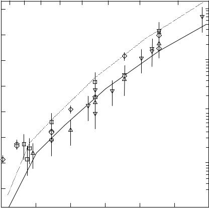
The systems Ag/W(110) and Ag/Fe(110) have been examined in detail with research students and other collaborators over a span of several years (Spiller et al. 1983, Jones & Venables 1985, Jones et al. 1990, Noro et al. 1995, 1996, Persaud et al. 1998). In these systems, 2ML of Ag form ®rst, and then ¯at Ag islands grow in (111) orientation. The experimental nucleation density N(T) is a strong function of substrate temperature, and the results of several Ag/W(110) experiments are shown in ®gure 5.13, in compar-
ison with a nucleation calculation nx(T) of the type outlined in section 5.2. In practice this proceeds by solving (5.14) iteratively, using the complete condensation solution as
the starting point.
Condensation is complete in this system, except at the highest temperatures studied, and the critical nucleus size is in the range 6±34, increasing with substrate temperature.
Energy values were deduced, Ea52.260.1, and the combination energy (Ed12Eb)5 0.6560.03 eV, within which Ed50.1560.1 and Eb50.257 0.05 eV (Jones et al. 1990). Note the errors are anti-correlated, since the combination energy is quite well deter-
mined by the absolute values of the data. What, however, makes these values interesting is that they can be compared with the best available calculations of metallic binding.
Comparison has been made with eVective medium theory, and the agreement is
166 5 Surface processes in epitaxial growth
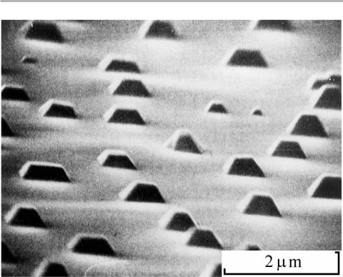
Figure 5.12. In situ UHV SEM pictures of nucleation and growth of Ag on Mo(001), shown after 20 ML was deposited at T5550°C (from Hartig et al. 1978, reproduced with permission).
striking, as shown in table 5.3 with other values later. In particular, the results demonstrate the non-linearity of metallic binding with increasing coordination number. In the simplest nearest neighbor bond model which we explored in chapter 1, the adsorption energy on (111) corresponds to 3 bonds, or half the sublimation energy for a f.c.c. crystal. So for Ag, with L52.95 eV, such a model would give Ea51.47 eV, whereas the actual value is much larger. The same eVect is at work in the high binding energy of Ag2 molecules, quoted in section 5.3.1 in connection with island growth experiments. However, the last bonds to form are much weaker, so that in this case Eb is much less than L/650.49 eV. This is a general feature of eVective medium or embedded atom calculations on metals, discussed further in section 6.1.
The comparison between Ag/W and Ag/Fe(110) shows that the ®rst two layers are diVerent crystallographically, with two distorted Ag(111)-like layers on W(110) (Bauer et al. 1977), compared to a missing row c531 structure for the ®rst layer, followed by an Ag(111)-like second layer on Fe(110) (Noro et al. 1995). But adatom behavior on top of these two layers is very similar. UHV SEM methods can visualize the ®rst and second MLs, and the islands on top of these MLs in ®nite deposits, using biased secondary electron imaging described in chapter 3. DiVusion in these systems is discussed in section 5.5.2. Some eVects in the ®rst MLs of the related, but rather more reactive systems Cu and Au deposited onto W and Mo(110) have been studied by LEEM
5.4 Metal deposition studied by UHV microscopies |
167 |
|
|
|
|
|
|
|
|
T (K) |
|
|
|
800 |
750 |
700 |
650 |
600 |
550 |
500 |
450 |
|
9.0 |
|
|
|
|
|
|
|
|
8.5 |
|
|
|
|
|
|
|
|
|
|
|
|
|
|
|
i = 6 |
|
8.0 |
|
|
|
|
|
|
|
|
|
|
|
|
|
|
i = 9 |
|
) |
7.5 |
|
|
|
|
|
|
|
|
|
|
|
|
|
|
|
|
2 |
|
|
|
|
|
|
|
|
/cm |
|
|
|
|
|
i = 17 |
|
|
(N |
|
|
|
|
|
|
|
|
Log |
7.0 |
|
|
|
|
|
|
|
|
|
|
|
|
|
|
|
|
|
6.5 |
|
|
i = 22 |
|
|
|
|
|
6.0 |
|
|
|
|
Ag/W (110) Jones et al. (1990) |
||
|
|
|
i = 34 |
|
|
Triangles, two samples `clean' |
||
|
|
|
|
|
Squares, `contaminated, stepped' |
|||
|
|
|
|
|
|
|||
|
5.5 |
|
|
|
|
Diamonds, Spiller et al. (1983) |
||
|
|
|
|
|
|
|
|
|
|
1.2 |
|
1.4 |
1.6 |
|
1.8 |
2.0 |
2.2 |
|
|
|
|
|
|
1000/T (1/K) |
|
|
109
108
107
106
2 /cmN
Figure 5.13. Arrhenius plot of nucleation density for silver islands on 2MLAg/W(110) with nucleation model superimposed. Full line: Ea52.1, Eb50.25, Ed50.135 eV, compared to data on the ¯attest, cleanest samples; dashed line: Ed50.185 eV, other parameters unchanged, compared to data on stepped and/or slightly contaminated samples. Deposition rate R5
0.3 ML/min (from Spiller et al. 1983, and Jones et al. 1990, reproduced with permission).
(Bauer 1997). Although one might attempt to extract detailed binding parameters from such kinetic observations, this has not been emphasized, possibly because of their complexity, including quite marked crystallographic anisotropy. Several of the adsorption energies are however known from older thermal desorption and other thermodynamic measurements (Bauer 1984).
5.4.2FIM studies of surface diffusion on metals
At the other end of the length scale, the ®eld ion microscope (FIM) has been used to study individual atomic jumps and the formation and motion of small clusters. These
168 5 Surface processes in epitaxial growth
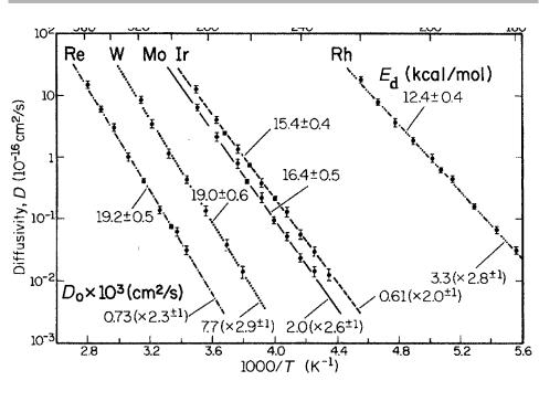
Figure 5.14. FIM measurements of surface diVusion of individual adatoms at a function of temperature on W(211), measured on the same sample. Note that energies Ed are quoted in kcal/mol (23.06 kcal/mol51 eV/atom). Errors in D0 are the factors in brackets (from Ehrlich 1991, after Wang & Ehrlich 1988, reproduced with permission).
observations are made at low temperature, with annealing at higher temperature for given times to eVect the jumps; the imaging ®eld is of course switched oV during the annealing periods. FIM works best for refractory metals, and high quality information has been obtained on diVusion coeYcients of individual atoms and small clusters in systems such as Re, W, Mo, Ir and Rh on tungsten, as shown in ®gure 5.14 for the W(211) surface (Ehrlich 1991, 1995, 1997). DiVusion on this surface is highly aniso-
Å
tropic, essentially moving along 1D channels parallel to the [011] direction, and avoiding jumps between channels. On higher symmetry surfaces, e.g. diVusion on (001) is observed to be isotropic, as it should be.
A particularly elegant application of FIM is to distinguish the hopping diVusion (pictured schematically in ®gure 5.3 and often assumed implicitly as the adatom diVusion mechanism) from exchange diVusion. If we draw a (001) surface of an f.c.c. crystal such as Pt, we know from chapter 1, problem 1.2, where an adatom will sit on this surface. So you can convince yourself that hopping diVusion will proceed in the close-packed K110L directions. By contrast, the exchange process consists of displacing a nearest neighbor of the adatom, and exchanging the adatom with it. The substrate atom `pops out' and the adatom becomes part of the substrate. In this case you can see that the direction of motion during diVusion is along K100L, at 45° to hopping diVusion