

5Surface processes in epitaxial growth
This chapter discusses models of nucleation and growth on surfaces, in the context of producing epitaxial thin ®lms. Section 5.1 gives some of the reasons for studying this topic and introduces some ideas needed as background. In section 5.2, we discuss diVerential equation formulations used to describe nucleation experiments quantitatively, and show how experiment±model comparisons can yield energies for characteristic surface processes. Sections 5.3 and 5.4 describe such comparisons in the case of metals growing on insulators and on metals. Section 5.5 explores steps, ripening and interdiVusion on insulator and metal surfaces. Although many of the same experiments and models are used in studying the growth of semiconductors, the role of surface reconstruction is much more important, so this topic is deferred to chapter 7.
5.1Introduction: growth modes and nucleation barriers
5.1.1Why are we studying epitaxial growth?
Epitaxial growth is a subject with considerable practical application, most obviously in relation to the production of semiconductor devices, but also to a whole range of other items. For example, magnetic devices such as recording heads have been produced by using metallic multilayers, in which alternating layers of magnetic and nonmagnetic materials produces high sensitivity to magnetic ®elds; other magnetic examples are bistable switches, where the alignment of the magnetic moments can be parallel or antiparallel in the neighboring layers. Many such ®lms are required to be single crystals with low defect density, and are produced via epitaxial growth processes. The term epitaxy has come to mean the growth of one layer in a particular crystallographic orientation relationship to the underlying, or substrate layer (Schneider & Ruth 1971, Bauer & Poppa 1972, Matthews 1975, Kern et al. 1979).
In most of these applications, the end-point interest is almost always electrical, magnetic or optical, and there may also be an interest in the mechanical properties; some of these features are explored in chapters 6±8. However, it is not enough to be interested just in the end-point, since we need to know how to get there, and what in¯uences the ®nal properties. It is here that the science behind the atomic and molecular processes in epitaxial growth can ®nd a good part of its (societal) justi®cation.
144
5.1 Introduction: growth modes and nucleation barriers |
145 |
|
|
However, in delving into this topic for its own sake, we should realize that the technological ends may be better served in other ways. For example, many multilayer ®lms are produced by sputtering, and are polycrystalline, albeit with a preferred orientation; another current example is that it may be better to produce ®lms by depositing (ionized) clusters rather than single atoms. A chapter which tried to interpret all the diVerent growth methods, including those listed in section 2.5, would look rather diVerent from this one.
5.1.2Simple models ± how far can we go?
In this situation, it seems a good idea to study a relatively simple approach in some depth. This enables one to say clearly what one does, and does not understand. Although it may help to oVer advice on what is or is not a good recipe for producing better ®lms or devices, this is certainly not straightforward. This dichotomy is an interesting example of the relationship between science and technology. It means that one can use the understanding so gained as background to appreciate the next technological advance, but that trying to advance the science and the technology are usually rather diVerent endeavors. But the role of scientists in producing new instruments such as the SEM, the STM or AFM should not be underestimated; such developments can completely change our perception of what is observable and interesting.
What is attempted here is to see how far one can go with simple models involving adsorption and diVusion of atoms, and the new element, binding between atoms on surfaces. Binding introduces cooperative features into the models, which are non-linear in the adatom concentration. This opens the way to a discussion of the kinetics of crystal nucleation and growth, as contrasted with the thermodynamics of adsorption studied in chapter 4. For both experiment and models, we can discuss these topics in atomistic terms; indeed the behavior of single atoms or molecules in¯uences the ®nal microstructure of thin ®lms in many cases.
The nucleation and growth patterns observed experimentally re¯ect directly the diVerent types of bonding in solids. Thus we can discuss what is expected in the growth of metals on metals, metals on ionic crystals or on semiconductors, and semiconductors on semiconductors. This subject has a long history, and a full literature citation is neither possible nor sensible in the present context. Growth and Properties of Ultrathin Epitaxial Layers (King & WoodruV 1997), Surface DiVusion: Atomistic and Collective Processes (Tringides 1997) and Thin Films: Heteroepitaxial Systems (Liu & Santos 1999) are recent research compilations; the main arguments are given here. One advantage of discussing this material in textbook form is that we can build on concepts, examples and problems discussed in earlier chapters using consistent notation. The great variety of notation is a major hazard in consulting the research literature directly.
5.1.3Growth modes and adsorption isotherms
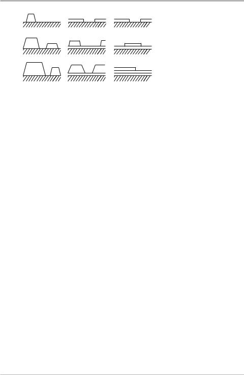
The classi®cation of three growth modes shown in ®gure 5.1 dates from a much quoted paper in Zeitschrift für Kristallographie (Bauer, 1958). The layer-by-layer, or
146 5 Surface processes in epitaxial growth
θ<1ML
1<θ<2
θ >2
(a) |
(b) |
(c) |
Figure 5.1. Schematic representation of the three growth modes, as a function of the coverage u in ML: (a) island, or Volmer±Weber growth; (b) layer-plus-island, or Stranski±Krastanov growth; (c) layer-by-layer, or Frank±van der Merwe growth (after Bauer 1958, and Venables et al. 1984, redrawn with permission).
Frank±van der Merwe, growth mode arises because the atoms of the deposit material are more strongly attracted to the substrate than they are to themselves. In the opposite case, where the deposit atoms are more strongly bound to each other than they are to the substrate, the island, or Volmer±Weber mode results. An intermediate case, the layer-plus-island, or Stranski±Krastanov (SK) growth mode is much more common than one might think. In this case, layers form ®rst, but then for one reason or another the system gets tired of this, and switches to islands.
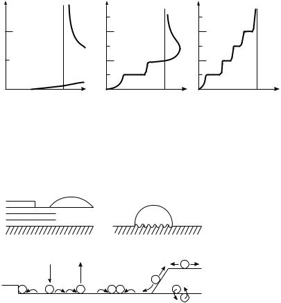
Bauer was the ®rst to systematize these (epitaxial) growth modes in terms of surface energies, similarly to earlier work on adhesion and contact angles by Young and Dupré. When we deposit material A on B, we get layer growth if gA,gB1g*, where g* is the interface energy, and vice versa for island growth. The SK mode arises because the interface energy increases as the layer thickness increases; typically this layer is strained to (more or less) ®t the substrate. Pseudomorphic growth is the term used when it ®ts exactly. For each of these growth modes, there is a corresponding adsorption isotherm, shown in ®gure 5.2. In the island growth mode, the adatom concentration on the surface is small at the equilibrium vapor pressure of the deposit; no deposit would occur at all unless one has a large supersaturation. In layer growth, the equilibrium vapor pressure is approached from below, so that all the kinetic processes occur at undersaturation, as in the discussion of adsorbed monolayers in section 4.3.1 In the SK mode, a ®nite number of layers are on the surface in equilibrium. The new element here is the idea of a nucleation barrier, shown as dashed lines on ®gure 5.2, which in the SK example occurs after the second ML has been formed, as opposed to after the ®rst ML in ®gure 5.1. The existence of such a barrier means that a ®nite supersaturation is required to nucleate the 3D deposit. Since these are kinetic phenomea, metastable (supersaturated) layers can also co-exist with the islands.
1Note that although it may be advisable to read chapter 4 ®rst, this is certainly not necessary. All the material in this chapter can be understood on the basis of chapter 1, especially section 1.3.
5.1 Introduction: growth modes and nucleation barriers |
147 |
|
|
u |
(a) |
(b) |
|
|
(c) |
1 |
4 |
|
|
|
4 |
|
2 |
|
|
|
2 |
0 |
0 |
|
± 0 |
|
0 |
|
±- 0 + |
|
+ |
±0 + |
|
|
|
|
|
|
Figure 5.2. Adsorption isotherms corresponding to the three growth modes shown in ®gure 5.1. Dm represents the chemical potential of the growing deposit relative to the bulk material, and u the coverage in ML. In (b) two stable intermediate layers are indicated (after Venables et al. 1984, redrawn with permisison).
(a) |
γ |
|
|
(b) |
|
|
|
A |
|
|
γ |
|
|
|
|
|
|
|
|
|
|
} |
γ |
|
B |
γ |
|
A |
* |
B |
γ* |
|||
|
|
|
A |
|||
B |
|
|
|
A |
|
|
(c) Arrival (R) |
|
Re-evaporation |
Surface |
|
||
|
|
|
|
diffusion |
|
|
|
|
|
|
E a |
|
|
|
E d |
E b |
|
|
||
Special |
Surface |
Binding, |
Interdiffusion |
|||
sites |
diffusion |
nucleation |
||||
Figure 5.3. (a) Growth of A on B, where gA,gB; mis®t dislocations are introduced, or islands form after a few layers have been deposited; (b) growth of B directly onto A as islands. The interfacial energy g* represents the excess energy over bulk A and B integrated through the interface region; (c) surface processes and characteristic energies in nucleation and ®lm growth (after Venables 1994, redrawn with permission).
5.1.4Nucleation barriers in classical and atomistic models
These phenomena look a lot more complex when one tries to compare this surface energy picture with what is going on at the atomic level, as shown schematically in ®gure 5.3. In ®gure 5.3(a) we see the deposition of A on B, and can visualize the way that islands form after a few layers due to the increase in g* with increasing ®lm thickness. If we grow B on A, as shown in ®gure 5.3(b), we get islands right away. Thus the growth of a multilayer ®lm A±B±A typically consists of alternate good and bad interfaces; there is no thermodynamic way to avoid this, though, as we shall see, kinetics plays a very important part in what actually happens.
If one looks at either interface in atomistic terms, as in ®gure 5.3(c), there are many

148 5 Surface processes in epitaxial growth
kinetic processes which can occur at both surfaces; in general only a few of these processes can be put into quantitative models at the same time. In particular, maybe only one (combination) of these processes will be rate-limiting, and thus be responsible for a nucleation barrier; this concept can be explored in both classical (macroscopic surface energy) or in atomistic terms.
Nucleation theory proceeds classically as follows. If we draw the case where gA.gB, so that we have 3D islands, as in ®gure 5.3(b), then we can construct a free energy diagram DG(j) for islands containing j atoms, which has the form
DG( j)52 jDm1j2/3X, at supersaturation Dm, |
(5.1a) |
where X is a surface energy term of the form |
|
X5okCkgk1CAB(g*2 gB ), |
(5.1b) |
where the ®rst term represents the surface energy of the various faces of the island A, and the second represents the interfacial energy between A and B; the geometrical constants Ck, CAB depend on the shape of the islands. Note that the reference state for which DG( j)50 is both a cluster containing no atoms ( j50), and also the bulk solid A in equilibrium with its own adsorbed layer and vapor, but where the surface energy is neglected, so that both Dm and X are zero; this second case was introduced in section 1.3 to de®ne Dm5kT ln(p/pe).
The form of such curves for diVerent values of Dm and X (in arbitrary units, but think kT) is shown in ®gure 5.4. The nucleation barrier results because there is a maximum in these curves, where the slope is zero. DiVerentiating, we can see that this
maximum occurs at j5i, where i is called the critical cluster size, and that |
|
i5(2X/3Dm)3 and DG(i)54X3/(27Dm2). |
(5.2) |
The same argument can be followed through for 2D clusters, i.e. monolayer thick islands. In this case, the relevant supersaturation is expressed in relation to the corresponding step in the adsorption isotherm, i.e. Dm95kT ln (p/p1) for nucleation of the ®rst monolayer. The form is now
DG( j)52 jDm91j1/2X, |
(5.3) |
where the square root expression results from the extra edge energy X. Finding the maximum in the same way leads to
i5(X/2Dm9)2 and DG(i)5X2/(4Dm9), |
(5.4) |
where Dm95Dm 2 Dmc and Dmc5(gA1g* ± gB)V2/3, with V as the atomic volume of the deposit. Thus, in this formulation, a measurement of the pressure of the steps in the
adsorption isotherm directly determines the surface energy diVerence (gA1g* ± gB). This way of looking at the problem is less than 100% realistic, perhaps not surpris-
ingly. It is rather arti®cial to think about surface energies of monolayers and very small clusters in terms of macroscopic concepts like surface energy. Numerically, the critical nucleus size, i, can be quite small, sometimes even one atom; this is the justi®cation for developing an atomistic model, as discussed in the next section. The form of the free