


100 3 Electron-based techniques
Figure 3.24. Cross sectional diagram of the specimen region of the MIDAS column, showing the relationship of parallelizer coils, objective lens, extraction optics and the sample (after Hembree & Venables 1992, reproduced with permission).
3.5.3Towards the highest spatial resolution: (a) SEM/STEM
The development of SEM/STEM and AES/SAM at the highest resolution has been pursued at Arizona State University in what has become known as the MIDAS project, a Microscope for Imaging, DiVraction and Analysis of Surfaces. Figures 3.24±3.27 are shown here to illustrate this project, which is described in more detail by Hembree & Venables (1992).
The innovation as regards electron optics is to use the spiraling of the low energy electrons in the high magnetic ®eld of the objective lens to contain the secondary and Auger electrons close to the microscope axis. These electrons are further controlled by auxiliary magnetic ®elds (parallelizers on ®gure 3.24) in the bores of the lens, and by biasing the sample negatively. A special combination Wien ®lter/de¯ector is then used to de¯ect the low energy electrons oV axis through a right angle, while keeping the 100 keV beam electrons on axis. The low energy electrons then enter a commercial CHA. Because they spiral in the high B ®eld and their angle to the axis decreases as the ®eld weakens, quite a large proportion of the emitted electrons can be collected. This higher collection angle compensates for the lower yield at higher beam energy, and the smaller current available in the ®ne probe.
The quality of the spectra obtained is relatively high, both with respect to energy resolution (®gure 3.25(a)) and to sensitivity (®gure 3.25(b)). Auger mapping is obtained by taking images A and B and using ratios (A2B)/(A1B) as explained above. Figure 3.26 shows the comparison of the b-SE image, with good SNR, and the Auger image, with relatively poor SNR, even after smoothing. For imaging, we have to be clear about distinctions between `image' and `analytical' resolution. This is because of the non-local

3.5 Microscopy-spectroscopy |
101 |
|
|
Intensity (cps)
100000
(a)
80000 |
60000
40000 |
Intensity (cps)
20000 |
|
|
|
1400 |
1500 |
1600 |
1700 |
Electron Energy (eV)
3000
(b)
2500
2000
1500
1000
500 |
|
|
|
|
|
3 2 0 |
3 4 0 |
3 6 0 |
3 8 0 |
4 0 0 |
4 2 0 |
Electron Energy (eV)
Figure 3.25. Pulse counted Auger electron spectra obtained with the 100 keV probe in MIDAS
(a) Si KLL from clean Si (10 nA probe current, 10 min acquisition time for 512 point spectrum); (b) Ag MNN from 100 nm wide island on Si(001) and from ,0.5 ML Ag layer between the islands (1.6 nA probe current, in 10 min (upper data) and 20 min (lower data) for the two cases respectively) (after Hembree & Venables 1992, reproduced with permission).

102 3 Electron-based techniques
20 nm
Ag Peak |
Background |
Ag MNN |
b-SEI |
Figure 3.26. Energy selected electron images, Ag MNN Auger intensity map derived from those images and biased secondary electron image of three-dimensional silver island on Si (001), with probe current 1.5 nA, 20 min acquisition time for energy selected images; 0.3 nA and 1 min for b-SEI (after Hembree & Venables 1992, reproduced with permission).
nature of the Auger signal, ®rstly from backscattered electrons as discussed already, but also at high spatial resolution because of the ®nite Auger attenuation length, and nonlocal excitation. Image resolutions below 3nm have been obtained on bulk samples in this instrument.
In the case of thin ®lm substrates, we largely eliminate the backscattering contribution, so that the image and analytical resolutions converge on the image resolution, which in practice may well be limited by the probe size. Such high resolutions are of interest in small particle research, particularly in catalysis. The old joke used to be that if you can see the particle in an electron microscope, then it was already too large to be a useful catalyst. Analysis of such a particle is even harder, especially if one is interested in minority elements. Work on such samples has been pursued by Liu et al. (1993) as illustrated in ®gure 3.27, which shows energy selected images of small Ag particles on a thin carbon substrate.
Here it is not so clear what the quanti®cation routine ought to be, and in practice Auger information has been portrayed using the raw A and B and simple diVerence (A2 B) images for various elements. Even for small Ag particles, backscattering eVects can be seen in the intensity of carbon Auger peak images (®gure 3.27(c) and (d)), but
3.5 Microscopy-spectroscopy |
103 |
|
|
( ) ( )
( ) |
( ) |
( ) |
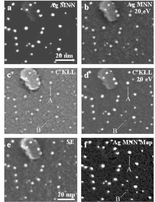
( ) |
Figure 3.27. Energy selected electron images of the same area containing small Ag particles on a thin amorphous carbon substrate obtained using diVerent signals in MIDAS: (a) Ag MNN;
(b) Ag MNN120 eV; (c) C KLL; (d) C KLL120 eV, (e) low energy SE, and (f) PAg 2 BAg (after Liu et al. 1993, reproduced with permission). The larger (A) and smaller (B) particles indicated in panels (c), (d) and(f) lie just oV the upper end of the corresponding drawn lines. See text for discussion.
1043 Electron-based techniques
the carbon background is largely removed in the Ag diVerence image (®gure 3.27(f)). Secondary electrons (®gure 3.27(e)) show a very similar information to energy selected images, via the higher secondary yield of Ag. Even more interesting is that, for particles of size at or below the Auger attenuation length, the number of atoms in the cluster is measured by the integrated intensity of the particle, rather than the image size of the particle, and that such images can be internally calibrated, using large particles such as A in ®gure 3.27(f). On this basis, it was concluded that particles such as B in this panel (clearly visible in the original, as all microscopists say) contained ,10 Ag atoms.
We should note that, because of the high yield for Ag MNN Auger electrons, this is a favorable case; we are still quite a way from detecting arbitrary minority species on such small particles. Moreover, we are much more likely to be able to detect them ®rst with a high SNR, qualitative, technique, such as b-SEI, than with low SNR, quantitative AES/SAM. There are more recent illustrations of this point coming from MIDAS. For example, oxygen KLL at 505 eV has a relatively low Auger yield. Small oxide particles on copper can be seen very readily in high resolution b-SE images. Indeed the presence of oxide can be seen in the shape of the (secondary electron) spectrum background, whereas wide beam Auger declares the surface to be clean (Heim et al. 1993). This discrepancy is due both to the fact that the oxide particles cover a small fraction of the surface, and that oxides in general have a very high secondary electron yield.
3.5.4Towards the highest spatial resolution: (b) scanned probe microscopy-spectroscopy
Following the revolutionary development of STM by Binnig, Rohrer and co-workers in 1982±83, it is now almost routine that atomic resolution can be obtained on a wide variety of samples, and, in contrast to the example described in the last section, many groups have achieved such resolution, even under UHV conditions. Indeed, these techniques are now so widespread that recent reviews of UHV-based STM have been specialized to particular materials, e.g. metals (Besenbacher 1996) or semiconductors (Kubby & Boland 1996, Neddermeyer 1996).
In my lecture courses, the use of spectroscopy in STM (or other scanned probe) instruments has typically been discussed in a student talk. In principle, such spectroscopic information allows one to identify surface atomic species in favorable cases, if not in general. This is because the STM/STS techniques (Feenstra 1994) probe the valence and conduction bands, which may be sensitive to atomic species, but are not chemical speci®c in the same sense as AES/SAM. This is not unlike the SEM/SAM distinction; STM/STS may well be able to perform `chemical' identi®cation possible out of a range of possibilities, due to a combination of atomic resolution and changes of contrast due to electronic eVects, and in particular due to a high SNR.
One of the many amazing positive features of STM/STS is that the probing current is also the signal, which may be between 1nA and 1pA. In AES/SAM used on a microscopic scale, the probing current may be between 100 nA and 10pA, but the collected current is down to maybe 100000 times smaller than the probe current, which does not do good things for the SNR. Thus one typically has to think very carefully about what