
- •1 Introduction
- •2 Description
- •3 Block diagram
- •4 Product overview
- •4.1 Single wire interface module (SWIM) and debug module (DM)
- •4.2 Interrupt controller
- •4.3 Flash program and data EEPROM memory
- •4.4 Clock controller
- •4.5 Power management
- •4.6 Watchdog timers
- •4.7 Auto wakeup counter
- •4.8 Beeper
- •4.13 Communication interfaces
- •4.13.1 UART2
- •5 Pinout and pin description
- •5.1 STM8S105 pinouts and pin description
- •5.1.1 Alternate function remapping
- •6 Memory and register map
- •6.1 Memory map
- •6.2 Register map
- •6.2.1 I/O port hardware register map
- •6.2.2 General hardware register map
- •6.2.3 CPU/SWIM/debug module/interrupt controller registers
- •7 Interrupt vector mapping
- •8 Option bytes
- •9 Unique ID
- •10 Electrical characteristics
- •10.1 Parameter conditions
- •10.1.1 Minimum and maximum values
- •10.1.2 Typical values
- •10.1.3 Typical curves
- •10.1.4 Typical current consumption
- •10.1.5 Loading capacitor
- •10.1.6 Pin input voltage
- •10.2 Absolute maximum ratings
- •10.3 Operating conditions
- •10.3.1 VCAP external capacitor
- •10.3.2 Supply current characteristics
- •10.3.2.1 Total current consumption in run mode
- •10.3.2.2 Total current consumption in wait mode
- •10.3.2.3 Total current consumption in active halt mode
- •10.3.2.4 Total current consumption in halt mode
- •10.3.2.5 Low power mode wakeup times
- •10.3.2.6 Total current consumption and timing in forced reset state
- •10.3.2.8 Current consumption curves
- •10.3.3 External clock sources and timing characteristics
- •10.3.4 Internal clock sources and timing characteristics
- •10.3.5 Memory characteristics
- •10.3.6 I/O port pin characteristics
- •10.3.7 Typical output level curves
- •10.3.8 Reset pin characteristics
- •10.3.9 SPI serial peripheral interface
- •10.3.10 I2C interface characteristics
- •10.3.12 EMC characteristics
- •10.3.12.1 Functional EMS (electromagnetic susceptibility)
- •10.3.12.2 Designing hardened software to avoid noise problems
- •10.3.12.3 Electromagnetic interference (EMI)
- •10.3.12.4 Absolute maximum ratings (electrical sensitivity)
- •10.3.12.5 Electrostatic discharge (ESD)
- •11 Package information
- •11.5 SDIP32 package mechanical data
- •12 Thermal characteristics
- •12.1 Reference document
- •12.2 Selecting the product temperature range
- •13 Ordering information
- •14 STM8S105 FASTROM microcontroller option list
- •15 STM8 development tools
- •15.2 Software tools
- •15.2.1 STM8 toolset
- •15.2.2 C and assembly toolchains
- •15.3 Programming tools
- •16 Revision history
- •17 Disclaimer

Electrical characteristics |
|
|
STM8S105xx |
|||
|
|
|
|
|
|
|
|
Symbol |
Parameter |
Conditions |
Min |
Max |
Unit |
|
|
|
VDD = 3.3 V |
|
|
|
|
|
|
|
|
|
|
|
|
Output low level with eight pins sunk |
IIO = 10 mA, |
|
0.9 |
|
|
|
|
VDD = 5 V |
|
|
|
|
|
|
|
|
|
|
|
|
Output low level with four pins sunk |
IIO = 20 mA, |
|
1.6 (1) |
|
|
|
|
VDD = 5 V |
|
|
|
|
|
|
|
|
|
|
|
VOH |
Output high level with four pins sourced |
IIO = 10 mA, |
1.9 (1) |
|
|
|
|
|
VDD = 3.3 V |
|
|
|
|
|
|
|
|
|
|
|
|
Output high level with eight pins sourced |
IIO = 10 mA, |
3.8 |
|
|
|
|
|
VDD = 5 V |
|
|
|
|
|
|
|
|
|
|
|
|
Output high level with four pins sourced |
IIO = 20 mA, |
2.9 (1) |
|
|
|
|
|
VDD = 5 V |
|
|
|
|
|
|
|
|
|
|
Notes:
(1) Data based on characterization results, not tested in production
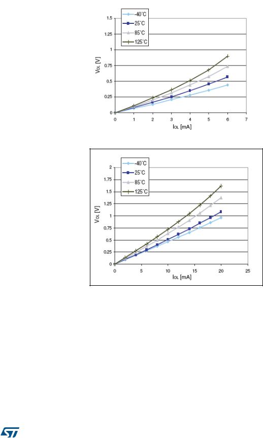
10.3.7Typical output level curves
The following figures show typical output level curves measured with output on a single pin.
Figure 27: Typ. VOL @ VDD = 5 V (standard ports)
64/99 |
DocID14771 Rev 13 |

STM8S105xx |
Electrical characteristics |
|
|
Figure 28: Typ. VOL @ VDD = 3.3 V (standard ports) |
|
|
|
|
|
|
|
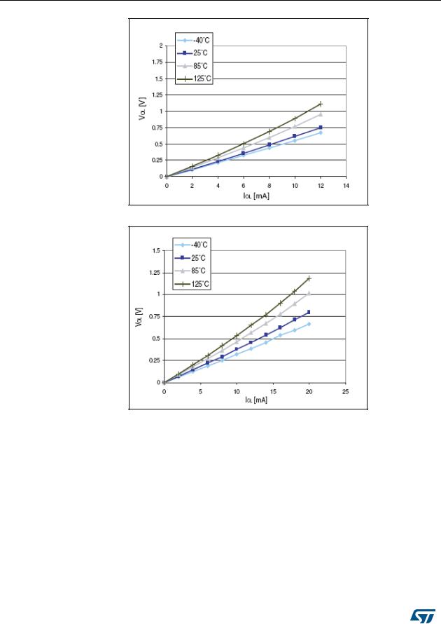
Figure 29: Typ. VOL @ VDD = 5 V (true open drain ports)
DocID14771 Rev 13 |
65/99 |

Electrical characteristics |
STM8S105xx |
Figure 30: Typ. VOL @ VDD = 3.3 V (true open drain ports)
Figure 31: Typ. VOL @ VDD = 5 V (high sink ports)
66/99 |
DocID14771 Rev 13 |

STM8S105xx |
Electrical characteristics |
|
|
Figure 32: Typ. VOL @ VDD = 3.3 V (high sink ports) |
|
|
|
|
|
|
|
Figure 33: Typ. VDD - VOH @ VDD = 5 V (standard ports)
Figure 34: Typ. VDD - VOH @ VDD = 3.3 V (standard ports)
DocID14771 Rev 13 |
67/99 |