

SPI Serial Interface
AT25010A/020A/040A |
6 AT25010A/020A/040A [Preliminary]
3402A–SEEPR–10/3/03

Functional
Description
3402A–SEEPR–10/3/03
AT25010A/020A/040A [Preliminary]
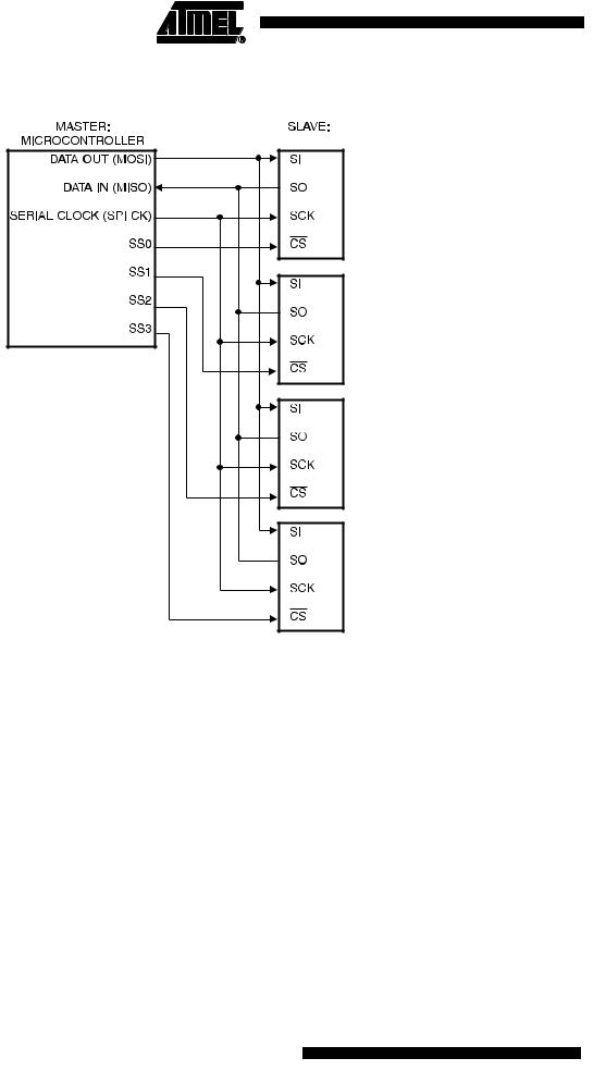
The AT25010A/020A/040A is designed to interface directly with the synchronous serial peripheral interface (SPI) of the 6805 and 68HC11 series of microcontrollers.
The AT25010A/020A/040A utilizes an 8-bit instruction register. The list of instructions and their operation codes are contained in Table 1. All instructions, addresses, and data are transferred with the MSB first and start with a high-to-low CS transition.
Table 1. Instruction Set for the AT25010A/020A/040A
Instruction Name |
Instruction Format |
Operation |
|
|
|
WREN |
0000 X110 |
Set Write Enable Latch |
|
|
|
WRDI |
0000 X100 |
Reset Write Enable Latch |
|
|
|
RDSR |
0000 X101 |
Read Status Register |
|
|
|
WRSR |
0000 X001 |
Write Status Register |
|
|
|
READ |
0000 A011 |
Read Data from Memory Array |
|
|
|
WRITE |
0000 A010 |
Write Data to Memory Array |
|
|
|
Note: “A” represents MSB address bit A8.
WRITE ENABLE (WREN): The device will power up in the write disable state when VCC is applied. All programming instructions must therefore be preceded by a Write
Enable instruction. The WP pin must be held high during a WREN instruction.
WRITE DISABLE (WRDI): To protect the device against inadvertent writes, the Write Disable instruction disables all programming modes. The WRDI instruction is independent of the status of the WP pin.
READ STATUS REGISTER (RDSR): The Read Status Register instruction provides access to the status register. The READY/BUSY and Write Enable status of the device can be determined by the RDSR instruction. Similarly, the Block Write Protection bits indicate the extent of protection employed. These bits are set by using the WRSR instruction.
Table 2. Status Register Format
Bit 7 |
Bit 6 |
Bit 5 |
Bit 4 |
Bit 3 |
Bit 2 |
Bit 1 |
Bit 0 |
|
|
|
|
|
|
|
|
|
|
|
|
X |
X |
X |
X |
BP1 |
BP0 |
WEN |
|
|
|
|
RDY |
|
|||||||
|
|
|
|
|
|
|
|
|
|
Table 3. Read Status Register Bit Definition
Bit |
|
|
|
Definition |
|||
|
|
|
|
|
|
|
|
|
|
|
|
Bit 0 = 0 |
|
indicates the device is READY. Bit 0 = 1 indicates the |
|
|
|
|
|
(RDY) |
|||
Bit 0 (RDY) |
|||||||
write cycle is in progress. |
|||||||
|
|
|
|
||||
|
|
|
|
|
|||
Bit 1 |
(WEN) |
Bit 1 = 0 indicates the device is not WRITE ENABLED. Bit 1 = 1 indicates |
|||||
the device is WRITE ENABLED. |
|||||||
|
|
|
|
||||
|
|
|
|||||
Bit 2 |
(BP0) |
See Table 4. |
|||||
|
|
|
|||||
Bit 3 |
(BP1) |
See Table 4. |
|||||
|
|
|
|
|
|
|
|
Bits 4-7 are 0s when device is not in an internal write cycle.
Bits 0-7 are 1s during an internal write cycle.
7

WRITE STATUS REGISTER (WRSR): The WRSR instruction allows the user to select one of four levels of protection. The AT25010A/020A/040A is divided into four array segments. Top quarter (1/4), Top half (1/2), or all of the memory segments can be protected. Any of the data within any selected segment will therefore be READ only. The block write protection levels and corresponding status register control bits are shown in Table 4.
The two bits, BP1 and BP0 are nonvolatile cells that have the same properties and functions as the regular memory cells (e.g. WREN, tWC, RDSR).
Table 4. Block Write Protect Bits
|
|
Status Register Bits |
|
Array Addresses Protected |
|
|||
|
|
|
|
|
|
|
|
|
Level |
BP1 |
BP0 |
AT25010A |
|
AT25020A |
|
AT25040A |
|
|
|
|
|
|
|
|
|
|
0 |
|
0 |
0 |
None |
|
None |
|
None |
|
|
|
|
|
|
|
|
|
1 (1/4) |
|
0 |
1 |
60-7F |
|
C0-FF |
|
180-1FF |
|
|
|
|
|
|
|
|
|
2 (1/2) |
|
1 |
0 |
40-7F |
|
80-FF |
|
100-1FF |
|
|
|
|
|
|
|
|
|
3 (All) |
1 |
1 |
00-7F |
|
00-FF |
|
000-1FF |
|
|
|
|
|
|
|
|
|
|
READ SEQUENCE (READ): Reading the AT25010A/020A/040A via the SO (Serial Output) pin requires the following sequence. After the CS line is pulled low to select a device, the READ op-code (including A8) is transmitted via the SI line followed by the byte address to be read (A7-A0). Upon completion, any data on the SI line will be ignored. The data (D7-D0) at the specified address is then shifted out onto the SO line. If only one byte is to be read, the CS line should be driven high after the data comes out. The READ sequence can be continued since the byte address is automatically incremented and data will continue to be shifted out. When the highest address is reached, the address counter will roll over to the lowest address allowing the entire memory to be read in one continuous READ cycle.
WRITE SEQUENCE (WRITE): In order to program the AT25010A/020A/040A, the Write Protect pin (WP) must be held high and two separate instructions must be executed. First, the device must be write enabled via the Write Enable (WREN) Instruction. Then a Write (WRITE) Instruction may be executed. Also, the address of the memory location(s) to be programmed must be outside the protected address field location selected by the Block Write Protection Level. During an internal write cycle, all commands will be ignored except the RDSR instruction.
A Write Instruction requires the following sequence. After the CS line is pulled low to select the device, the WRITE op-code (including A8) is transmitted via the SI line followed by the byte address (A7-A0) and the data (D7-D0) to be programmed. Programming will start after the CS pin is brought high. (The LOW to High transition of the CS pin must occur during the SCK low time immediately after clocking in the D0 (LSB) data bit.
The READY/BUSY status of the device can be determined by initiating a READ STATUS REGISTER (RDSR) Instruction. If Bit 0 = 1, the WRITE cycle is still in progress. If Bit 0 = 0, the WRITE cycle has ended. Only the READ STATUS REGISTER instruction is enabled during the WRITE programming cycle.
8 AT25010A/020A/040A [Preliminary]
3402A–SEEPR–10/3/03

 AT25010A/020A/040A [Preliminary]
The AT25010A/020A/040A is capable of an 8-byte PAGE WRITE operation. After each byte of data is received, the three low order address bits are internally incremented by one; the six high order bits of the address will remain constant. If more than 8 bytes of data are transmitted, the address counter will roll over and the previously written data will be overwritten. The AT25010A/020A/040A is automatically returned to the write disable state at the completion of a WRITE cycle.
NOTE: If the WP pin is brought low or if the device is not Write enabled (WREN), the device will ignore the Write instruction and will return to the standby state, when CS is brought high. A new CS falling edge is required to re-initiate the serial communication.
9
3402A–SEEPR–10/3/03