

Features
•Serial Peripheral Interface (SPI) Compatible
•Supports SPI Modes 0 (0,0) and 3 (1,1)
•Medium-voltage and Standard-voltage Operation
–5.0 (VCC = 4.5V to 5.5V)
–2.7 (VCC = 2.7V to 5.5V)
•3.0 MHz Clock Rate (5V)
•32-byte Page Mode
•Block Write Protection
–Protect 1/4, 1/2, or Entire Array
•Write Protect (WP) Pin and Write Disable Instructions for both Hardware and Software Data Protection
•Self-timed Write Cycle (5 ms Typical)
•High-reliability
–Endurance: One Million Write Cycles
–Data Retention: 100 Years
•8-lead PDIP and 8-lead JEDEC SOIC Packages
Description
The AT25080/160/320/640 provides 8192/16384/32768/65536 bits of serial electri- cally-erasable programmable read only memory (EEPROM) organized as 1024/2048/4096/8192 words of 8 bits each. The device is optimized for use in many automotive applications where low-power and low-voltage operation are essential. The AT25080/160/320/640 is available in space saving 8-lead PDIP and 8-lead JEDEC SOIC packages.
The AT25080/160/320/640 is enabled through the Chip Select pin (CS) and accessed via a 3-wire interface consisting of Serial Data Input (SI), Serial Data Output (SO), and Serial Clock (SCK). All programming cycles are completely self-timed, and no separate ERASE cycle is required before WRITE.
BLOCK WRITE protection is enabled by programming the status register with one of four blocks of write protection. Separate program enable and program disable instructions are provided for additional data protection. Hardware data protection is provided via the WP pin to protect against inadvertent write attempts to the status register. The HOLD pin may be used to suspend any serial communication without resetting the serial sequence.
Pin Configuration
|
Pin Name |
Function |
|
|
|
|
|
|
|
|
|
|
|
|
|
|
|
|
|
|
|
|
|
|
|
|
|
|||
|
|
|
|
|
|
|
|
|
|
|
8-lead PDIP |
|
|
|
|
|
|
|
|
|
8-lead SOIC |
|
|
|
||||||
|
|
|
|
|
|
|
|
|
|
|
|
|
|
|
|
|
|
|
|
|
|
|
||||||||
|
CS |
Chip Select |
|
|
|
|
|
|
|
|
|
|
|
|
|
|
|
|
|
|||||||||||
|
|
|
|
|
|
|
|
|
|
|
|
|
|
|
|
|
|
|
|
|
|
|
|
|
|
|||||
|
SCK |
Serial Data Clock |
|
|
|
|
1 |
8 |
|
VCC |
|
|
|
|
|
|
|
1 |
8 |
|
VCC |
|||||||||
|
|
|
CS |
|
|
|
|
|
|
|
CS |
|
|
|
||||||||||||||||
|
|
|
|
|
|
|
||||||||||||||||||||||||
|
|
|
|
|
|
|
||||||||||||||||||||||||
|
|
|
|
|
|
|
SO |
|
2 |
7 |
|
|
HOLD |
|
|
|
|
SO |
|
2 |
7 |
|
|
HOLD |
|
|||||
|
|
|
|
|
|
|
|
|
|
|
|
|||||||||||||||||||
|
SI |
Serial Data Input |
|
|
||||||||||||||||||||||||||
|
|
|
|
|
|
|
|
|
|
|
|
|
|
|
|
|
|
|
|
|
|
|||||||||
|
|
WP |
|
3 |
6 |
|
SCK |
|
|
|
WP |
|
3 |
6 |
|
SCK |
||||||||||||||
|
|
|
|
|
|
|
||||||||||||||||||||||||
|
|
|
|
|
|
GND |
|
4 |
5 |
|
SI |
|
|
GND |
|
4 |
5 |
|
SI |
|||||||||||
|
SO |
Serial Data Output |
|
|
|
|
|
|
|
|
|
|
|
|
|
|
|
|
|
|
|
|
|
|
|
|
|
|||
|
|
|
|
|
|
|
|
|
|
|
|
|
|
|
|
|
|
|
|
|
|
|
|
|
|
|
|
|
|
|
|
GND |
Ground |
|
|
|
|
|
|
|
|
|
|
|
|
|
|
|
|
|
|
|
|
|
|
|
|
|
|||
|
|
|
|
|
|
|
|
|
|
|
|
|
|
|
|
|
|
|
|
|
|
|
|
|
|
|
|
|||
|
VCC |
Power Supply |
|
|
|
|
|
|
|
|
|
|
|
|
|
|
|
|
|
|
|
|
|
|
|
|
|
|||
|
|
|
|
|
|
|
|
|
|
|
|
|
|
|
|
|
|
|
|
|
|
|
|
|
|
|
|
|
|
|
|
|
|
|
|
Write Protect |
|
|
|
|
|
|
|
|
|
|
|
|
|
|
|
|
|
|
|
|
|
|
|
|
|
|
WP |
|
|
|
|
|
|
|
|
|
|
|
|
|
|
|
|
|
|
|
|
|
|
|
|
|
||||
|
|
|
|
|
|
|
|
|
|
|
|
|
|
|
|
|
|
|
|
|
|
|
|
|
|
|
|
|
||
|
|
|
|
|
Suspends Serial Input |
|
|
|
|
|
|
|
|
|
|
|
|
|
|
|
|
|
|
|
|
|
|
|
|
|
|
HOLD |
|
|
|
|
|
|
|
|
|
|
|
|
|
|
|
|
|
|
|
|
|
|
|
|
|
||||
|
|
|
|
|
|
|
|
|
|
|
|
|
|
|
|
|
|
|
|
|
|
|
|
|
|
|
|
|||
|
NC |
No Connect |
|
|
|
|
|
|
|
|
|
|
|
|
|
|
|
|
|
|
|
|
|
|
|
|
|
|||
|
|
|
|
|
|
|
|
|
|
|
|
|
|
|
|
|
|
|
|
|
|
|
|
|
|
|
|
|||
|
DC |
Don’t Connect |
|
|
|
|
|
|
|
|
|
|
|
|
|
|
|
|
|
|
|
|
|
|
|
|
|
|||
|
|
|
|
|
|
|
|
|
|
|
|
|
|
|
|
|
|
|
|
|
|
|
|
|
|
|
|
|
|
|
|
|
|
|
|
|
|
|
|
|
|
|
|
|
|
|
|
|
|
|
|
|
|
|
|
|
|
|
|
|
|
|
|
|
|
|
|
|
|
|
|
|
|
|
|
|
|
|
|
|
|
|
|
|
|
|
|
|
|
|
|
|
|
|
|
|
|
|
|
|
|
|
|
|
|
|
|
|
|
|
|
|
|
|
|
|
|
|
|
|
|
|
|
SPI Serial |
Automotive |
EEPROMs |
8K (1024 x 8) |
16K (2048 x 8) |
32K (4096 x 8) |
64K (8192 x 8) |
AT25080 |
AT25160 |
AT25320 |
AT25640 |
3260D–SEEPR–9/03 |
1 |
Absolute Maximum Ratings*
..................................Operating Temperature |
-55°C to +125°C |
*NOTICE: Stresses beyond those listed under “Absolute |
|
|
Maximum Ratings” may cause permanent dam- |
Storage Temperature ..................................... |
-65°C to +150°C |
age to the device. This is a stress rating only and |
|
|
functional operation of the device at these or any |
Voltage on Any Pin |
|
other conditions beyond those indicated in the |
with Respect to Ground ..................................... |
-1.0V to +7.0V |
operational sections of this specification is not |
|
|
implied. Exposure to absolute maximum rating |
Maximum Operating Voltage .......................................... |
6.25V |
conditions for extended periods may affect device |
DC Output Current |
5.0 mA |
reliability. |
|
||
|
|
|
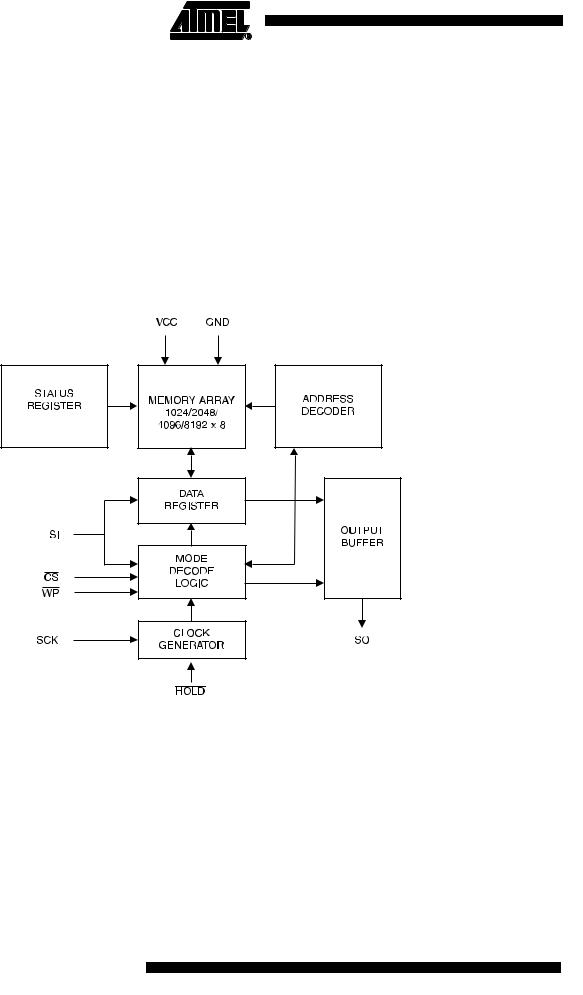
Block Diagram
2 AT25080/160/320/640
3260D–SEEPR–9/03

AT25080/160/320/640
Pin Capacitance(1)
Applicable over recommended operating range from TA = 25°C, f = 1.0 MHz, VCC = +5.0V (unless otherwise noted).
Symbol |
|
Test Conditions |
Max |
Units |
Conditions |
||||||
|
|
|
|
|
|
||||||
COUT |
|
Output Capacitance (SO) |
8 |
pF |
VOUT = 0V |
||||||
CIN |
|
Input Capacitance |
|
SCK, SI, |
|
|
|
|
6 |
pF |
VIN = 0V |
(CS, |
WP, |
HOLD) |
|||||||||
Note: 1. |
This parameter is characterized and is not 100% tested. |
|
|
|
|||||||
DC Characteristics(1)
Applicable over recommended operating range from: TA = -40°C to +125°C, VCC = +2.7V to +5.5V
Symbol |
|
Parameter |
Test Condition |
|
Min |
Typ |
Max |
Units |
|||
|
|
|
|
|
|
|
|
|
|
|
|
VCC1 |
|
Supply Voltage |
|
|
|
|
|
2.7 |
|
5.5 |
V |
VCC2 |
|
Supply Voltage |
|
|
|
|
|
4.5 |
|
5.5 |
V |
ICC1 |
|
Supply Current |
VCC = 5.0V at 1 MHz, SO = Open, Read |
|
|
3.0 |
mA |
||||
ICC2 |
|
Supply Current |
VCC = 5.0V at 2 MHz, SO = Open, |
|
|
5.0 |
mA |
||||
|
|
|
Read, Write |
|
|
|
|
|
|||
|
|
|
|
|
|
|
|
|
|
|
|
ISB1 |
|
Standby Current |
VCC = 2.7V, |
|
= VCC |
|
|
0.2 |
2.0 |
µA |
|
CS |
|
|
|||||||||
ISB2 |
|
Standby Current |
VCC = 5.0V, |
|
= VCC |
|
|
2.0 |
5.0 |
µA |
|
CS |
|
|
|||||||||
IIL |
|
Input Leakage |
VIN = 0V to VCC |
|
-3.0 |
|
|
µA |
|||
IOL |
|
Output Leakage |
VIN = 0V to VCC |
|
-3.0 |
|
3.0 |
µA |
|||
VIL(1) |
|
Input Low-voltage |
|
|
|
|
|
-0.6 |
|
VCC x 0.3 |
V |
VIH(1) |
|
Input High-voltage |
|
|
|
|
|
VCC x 0.7 |
|
VCC + 0.5 |
V |
VOL1 |
|
Output Low-voltage |
2.7V ≤ VCC ≤ 5.5V |
IOL = 3.0 mA |
|
|
0.4 |
V |
|||
VOH1 |
|
Output High-voltage |
|
|
|
|
IOH = -1.6 mA |
VCC - 0.8 |
|
|
V |
Note: 1. |
VIL min and VIH max are reference only and are not tested. |
|
|
|
|
||||||
3
3260D–SEEPR–9/03

AC Characteristics
Applicable over recommended operating range from TA = -40°C to +125°C, VCC = As Specified, CL = 1 TTL Gate and 100 pF (unless otherwise noted).
Symbol |
|
Parameter |
Voltage |
Min |
Max |
Units |
||
|
|
|
|
|
|
|
||
fSCK |
|
SCK Clock Frequency |
4.5 - 5.5 |
0 |
3.0 |
MHz |
||
|
|
|
|
|
2.7 - 5.5 |
0 |
2.1 |
|
|
|
|
|
|
|
|
||
tRI |
|
Input Rise Time |
4.5 - 5.5 |
|
2 |
µs |
||
|
|
|
|
|
2.7 - 5.5 |
|
2 |
|
|
|
|
|
|
|
|
||
tFI |
|
Input Fall Time |
4.5 - 5.5 |
|
2 |
µs |
||
|
|
|
|
|
2.7 - 5.5 |
|
2 |
|
|
|
|
|
|
|
|
||
tWH |
|
SCK High Time |
4.5 - 5.5 |
133 |
|
ns |
||
|
|
|
|
|
2.7 - 5.5 |
200 |
|
|
|
|
|
|
|
|
|
||
tWL |
|
SCK Low Time |
4.5 - 5.5 |
133 |
|
ns |
||
|
|
|
|
|
2.7 - 5.5 |
200 |
|
|
|
|
|
|
|
|
|
|
|
tCS |
|
|
High Time |
4.5 - 5.5 |
250 |
|
ns |
|
CS |
|
|||||||
|
|
|
|
|
2.7 - 5.5 |
250 |
|
|
|
|
|
|
|
|
|
|
|
tCSS |
|
|
Setup Time |
4.5 - 5.5 |
250 |
|
ns |
|
CS |
|
|||||||
|
|
|
|
|
2.7 - 5.5 |
250 |
|
|
|
|
|
|
|
|
|
|
|
tCSH |
|
|
Hold Time |
4.5 - 5.5 |
250 |
|
ns |
|
CS |
|
|||||||
|
|
|
|
|
2.7 - 5.5 |
250 |
|
|
|
|
|
|
|
|
|
||
tSU |
|
Data In Setup Time |
4.5 - 5.5 |
50 |
|
ns |
||
|
|
|
|
|
2.7 - 5.5 |
50 |
|
|
|
|
|
|
|
|
|
||
tH |
|
Data In Hold Time |
4.5 - 5.5 |
50 |
|
ns |
||
|
|
|
|
|
2.7 - 5.5 |
50 |
|
|
|
|
|
|
|
|
|
|
|
tHD |
|
|
|
Setup Time |
4.5 - 5.5 |
100 |
|
|
Hold |
|
|
||||||
|
|
|
|
|
2.7 - 5.5 |
100 |
|
|
|
|
|
|
|
|
|
|
|
tCD |
|
|
|
Hold Time |
4.5 - 5.5 |
200 |
|
ns |
Hold |
|
|||||||
|
|
|
|
|
2.7 - 5.5 |
200 |
|
|
|
|
|
|
|
|
|
||
tV |
|
Output Valid |
4.5 - 5.5 |
0 |
133 |
ns |
||
|
|
|
|
|
2.7 - 5.5 |
0 |
200 |
|
|
|
|
|
|
|
|
||
tHO |
|
Output Hold Time |
4.5 - 5.5 |
0 |
|
ns |
||
|
|
|
|
|
2.7 - 5.5 |
0 |
|
|
|
|
|
|
|
|
|
|
|
tLZ |
|
|
|
to Output Low Z |
4.5 - 5.5 |
0 |
100 |
ns |
Hold |
||||||||
|
|
|
|
|
2.7 - 5.5 |
0 |
100 |
|
|
|
|
|
|
|
|
|
|
tHZ |
|
|
|
to Output High Z |
4.5 - 5.5 |
|
100 |
ns |
Hold |
|
|||||||
|
|
|
|
|
2.7 - 5.5 |
|
100 |
|
|
|
|
|
|
|
|
||
tDIS |
|
Output Disable Time |
4.5 - 5.5 |
|
250 |
ns |
||
|
|
|
|
|
2.7 - 5.5 |
|
250 |
|
|
|
|
|
|
|
|
||
tWC |
|
Write Cycle Time |
4.5 - 5.5 |
|
5 |
ms |
||
|
|
|
|
|
2.7 - 5.5 |
|
10 |
|
|
|
|
|
|
|
|
||
Endurance(1) |
|
5.0V, 25°C, Page Mode |
|
1M |
|
Write Cycles |
||
Note: 1. This parameter is characterized and is not 100% tested.
4 AT25080/160/320/640
3260D–SEEPR–9/03

Serial Interface
Description
3260D–SEEPR–9/03
AT25080/160/320/640
MASTER: The device that generates the serial clock.
SLAVE: Because the Serial Clock pin (SCK) is always an input, the AT25080/160/320/640 always operates as a slave.
TRANSMITTER/RECEIVER: The AT25080/160/320/640 has separate pins designated for data transmission (SO) and reception (SI).
MSB: The Most Significant Bit (MSB) is the first bit transmitted and received.
SERIAL OP-CODE: After the device is selected with CS going low, the first byte will be received. This byte contains the op-code that defines the operations to be performed.
INVALID OP-CODE: If an invalid op-code is received, no data will be shifted into the AT25080/160/320/640, and the serial output pin (SO) will remain in a high impedance state until the falling edge of CS is detected again. This will reinitialize the serial communication.
CHIP SELECT: The AT25080/160/320/640 is selected when the CS pin is low. When the device is not selected, data will not be accepted via the SI pin, and the serial output pin (SO) will remain in a high impedance state.
H O L D : Th e H O L D p i n is u s e d i n c o n j u n c t i o n w i t h t h e C S p in t o s e l e c t t h e AT25080/160/320/640. When the device is selected and a serial sequence is underway, HOLD can be used to pause the serial communication with the master device without resetting the serial sequence. To pause, the HOLD pin must be brought low while the SCK pin is low. To resume serial communication, the HOLD pin is brought high while the SCK pin is low (SCK may still toggle during HOLD). Inputs to the SI pin will be ignored while the SO pin is in the high impedance state.
WRITE PROTECT: The write protect pin (WP) will allow normal read/write operations when held high. When the WP pin is brought low and WPEN bit is “1”, all write operations to the status register are inhibited. WP going low while CS is still low will interrupt a write to the status register. If the internal write cycle has already been initiated, WP going low will have no effect on any write operation to the status register. The WP pin function is blocked when the WPEN bit in the status register is "0". This will allow the user to install the AT25080/160/320/640 in a system with the WP pin tied to ground and still be able to write to the status register. All WP pin functions are enabled when the WPEN bit is set to “1”.
5
SPI Serial
Interface
6 AT25080/160/320/640
3260D–SEEPR–9/03

Functional
Description
3260D–SEEPR–9/03
AT25080/160/320/640
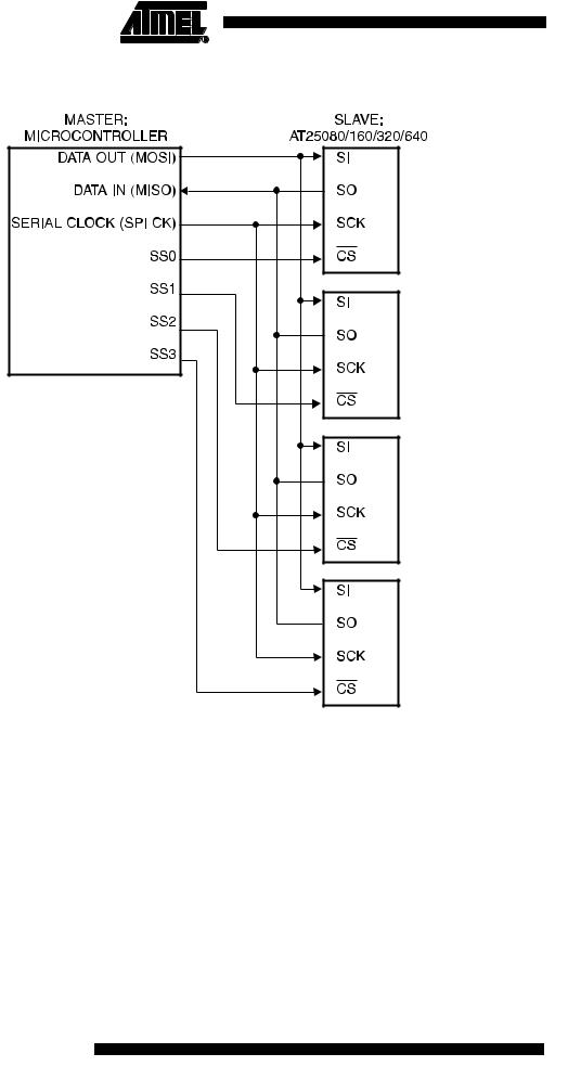
The AT25080/160/320/640 is designed to interface directly with the synchronous serial peripheral interface (SPI) of the 6805 and 68HC11 series of microcontrollers.
The AT25080/160/320/640 utilizes an 8-bit instruction register. The list of instructions and their operation codes are contained in Table 1. All instructions, addresses, and data are transferred with the MSB first and start with a high-to-low CS transition.
Table 1. Instruction Set for the AT25080/160/320/640
Instruction Name |
Instruction Format |
Operation |
|
|
|
WREN |
0000 X110 |
Set Write Enable Latch |
|
|
|
WRDI |
0000 X100 |
Reset Write Enable Latch |
|
|
|
RDSR |
0000 X101 |
Read Status Register |
|
|
|
WRSR |
0000 X001 |
Write Status Register |
|
|
|
READ |
0000 X011 |
Read Data from Memory Array |
|
|
|
WRITE |
0000 X010 |
Write Data to Memory Array |
|
|
|
WRITE ENABLE (WREN): The device will power-up in the write disable state when VCC is applied. All programming instructions must therefore be preceded by a Write Enable instruction.
WRITE DISABLE (WRDI): To protect the device against inadvertent writes, the Write Disable instruction disables all programming modes. The WRDI instruction is independent of the status of the WP pin.
READ STATUS REGISTER (RDSR): The Read Status Register instruction provides access to the status register. The READY/BUSY and Write Enable status of the device can be determined by the RDSR instruction. Similarly, the Block Write Protection bits indicate the extent of protection employed. These bits are set by using the WRSR instruction.
Table 2. Status Register Format
Bit 7 |
Bit 6 |
Bit 5 |
Bit 4 |
Bit 3 |
Bit 2 |
Bit 1 |
Bit 0 |
||
|
|
|
|
|
|
|
|
|
|
WPEN |
X |
X |
X |
BP1 |
BP0 |
WEN |
|
|
|
|
RDY |
||||||||
|
|
|
|
|
|
|
|
|
|
Table 3. Read Status Register Bit Definition
Bit |
|
|
|
Definition |
||
|
|
|
|
|
|
|
Bit 0 |
|
|
Bit 0 = 0 |
|
indicates the device is READY. Bit 0 = 1 indicates the write cycle is |
|
(RDY) |
(RDY) |
|||||
|
|
|
|
in progress. |
||
|
|
|||||
Bit 1 (WEN) |
Bit 1= 0 indicates the device is not WRITE ENABLED. Bit 1 = 1 indicates the |
|||||
|
|
|
|
device is WRITE ENABLED. |
||
|
|
|
||||
Bit 2 |
(BP0) |
See Table 4 on page 8. |
||||
|
|
|
||||
Bit 3 |
(BP1) |
See Table 4 on page 8. |
||||
|
|
|||||
Bits 4 - 6 are 0s when device is not in an internal write cycle. |
||||||
|
|
|
||||
Bit 7 |
(WPEN) |
See Table 5 on page 8. |
||||
|
|
|
|
|
|
|
Bits 0 - 7 are 1s during an internal write cycle.
7

WRITE STATUS REGISTER (WRSR): The WRSR instruction allows the user to select one of four levels of protection. The AT25080/160/320/640 is divided into four array segments. One quarter (1/4), one half (1/2), or all of the memory segments can be protected. Any of the data within any selected segment will therefore be READ only. The block write protection levels and corresponding status register control bits are shown in Table 4.
The three bits, BP0, BP1, and WPEN are nonvolatile cells that have the same properties and functions as the regular memory cells (e.g. WREN, tWC, RDSR).
Table 4. Block Write Protect Bits
|
Status |
|
|
|
|
|
|
Register Bits |
|
Array Addresses Protected |
|
||
|
|
|
|
|
|
|
Level |
BP1 |
BP0 |
AT25080 |
AT25160 |
AT25320 |
AT25640 |
|
|
|
|
|
|
|
0 |
0 |
0 |
None |
None |
None |
None |
|
|
|
|
|
|
|
1(1/4) |
0 |
1 |
0300 |
0600 |
0C00 |
1800 |
|
-03FF |
-07FF |
-0FFF |
-1FFF |
||
|
|
|
||||
|
|
|
|
|
|
|
2(1/2) |
1 |
0 |
0200 |
0400 |
0800 |
1000 |
|
-03FF |
-07FF |
-0FFF |
-1FFF |
||
|
|
|
||||
|
|
|
|
|
|
|
3(All) |
1 |
1 |
0000 |
0000 |
0000 |
0000 |
|
-03FF |
-07FF |
-0FFF |
-1FFF |
||
|
|
|
||||
|
|
|
|
|
|
|
The WRSR instruction also allows the user to enable or disable the write protect (WP) pin through the use of the Write Protect Enable (WPEN) bit. Hardware write protection is enabled when the WP pin is low and the WPEN bit is “1”. Hardware write protection is disabled when either the WP pin is high or the WPEN bit is “0”When. the device is hardware write protected, writes to the Status Register, including the Block Protect bits and the WPEN bit, and the blockprotected sections in the memory array are disabled. Writes are only allowed to sections of the memory which are not block-protected.
NOTE: When the WPEN bit is hardware write protected, it cannot be changed back to “0”, as long as the WP pin is held low.
Table 5. WPEN Operation
|
|
|
|
|
Protected |
Unprotected |
Status |
WPEN |
|
|
|
WEN |
Blocks |
Blocks |
Register |
|
WP |
||||||
|
|
|
|
|
|
|
|
0 |
|
X |
0 |
Protected |
Protected |
Protected |
|
|
|
|
|
|
|
|
|
0 |
|
X |
1 |
Protected |
Writable |
Writable |
|
|
|
|
|
|
|
||
1 |
Low |
0 |
Protected |
Protected |
Protected |
||
|
|
|
|
|
|
||
1 |
Low |
1 |
Protected |
Writable |
Protected |
||
|
|
|
|
|
|
||
X |
High |
0 |
Protected |
Protected |
Protected |
||
|
|
|
|
|
|
||
X |
High |
1 |
Protected |
Writable |
Writable |
||
|
|
|
|
|
|
|
|
8 AT25080/160/320/640
3260D–SEEPR–9/03

 AT25080/160/320/640
READ SEQUENCE (READ): Reading the AT25080/160/320/640 via the SO (Serial Output) pin requires the following sequence. After the CS line is pulled low to select a device, the READ op-code is transmitted via the SI line followed by the byte address to be read (A15 - A0, Refer to Table 6). Upon completion, any data on the SI line will be ignored. The data (D7 - D0) at the specified address is then shifted out onto the SO line. If only one byte is to be read, the CS line should be driven high after the data comes out. The READ sequence can be continued since the byte address is automatically incremented and data will continue to be shifted out. When the highest address is reached, the address counter will roll over to the lowest address allowing the entire memory to be read in one continuous READ cycle.
WRITE SEQUENCE (WRITE): In order to program the AT25080/160/320/640, two separate instructions must be executed. First, the device must be write enabled via the Write Enable (WREN) Instruction. Then a Write (WRITE) Instruction may be executed. Also, the address of the memory location(s) to be programmed must be outside the protected address field location selected by the Block Write Protection Level. During an internal write cycle, all commands will be ignored except the RDSR instruction.
A Write Instruction requires the following sequence. After the CS line is pulled low to select the device, the WRITE op-code is transmitted via the SI line followed by the byte address (A15 - A0) and the data (D7 - D0) to be programmed (Refer to Table 6). Programming will start after the CS pin is brought high. The Low-to-High transition of the CS pin must occur during the SCK low-time immediately after clocking in the D0 (LSB) data bit.
The READY/BUSY status of the device can be determined by initiating a READ STATUS REGISTER (RDSR) Instruction. If Bit 0 = 1, the WRITE cycle is still in progress. If Bit 0 = 0, the WRITE cycle has ended. Only the READ STATUS REGISTER instruction is enabled during the WRITE programming cycle.
The AT25080/160/320/640 is capable of a 32-byte PAGE WRITE operation. After each byte of data is received, the five low order address bits are internally incremented by one; the high order bits of the address will remain constant. If more than 32 bytes of data are transmitted, the address counter will roll over and the previously written data will be overwritten. The AT25080/160/320/640 is automatically returned to the write disable state at the completion of a WRITE cycle.
NOTE: If the device is not Write enabled (WREN), the device will ignore the Write instruction and will return to the standby state, when CS is brought high. A new CS falling edge is required to re-initiate the serial communication.
Table 6. Address Key
Address |
AT25080 |
AT25160 |
AT25320 |
AT25640 |
|
|
|
|
|
|
|
AN |
A9 - A0 |
A10 - A0 |
A11 - A0 |
A12 - A0 |
|
Don't |
A15 - A10 |
A15 - A11 |
A15 - A12 |
A15 - A13 |
|
Care Bits |
|||||
|
|
|
|
||
|
|
|
|
|
9
3260D–SEEPR–9/03