

AT25080/160/320/640
Packaging Information
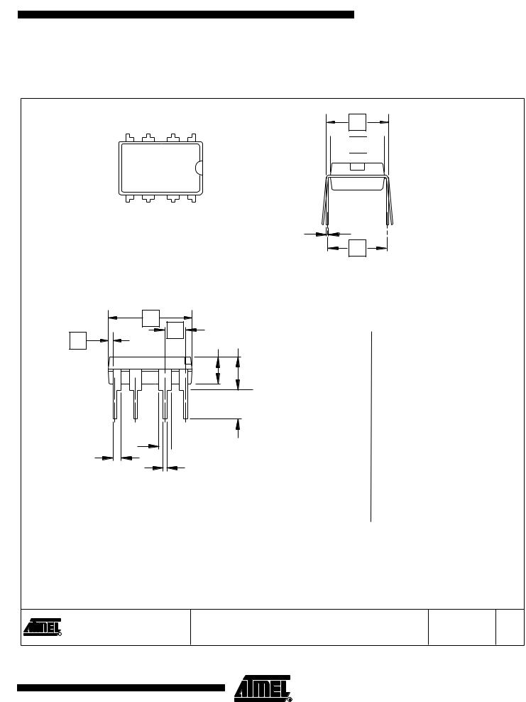
8P3 – PDIP
1 |
E |
|

 E1
E1 

|
N |
Top View |
c |
|
eA |
|
End View |
D
e
D1 |
A2 A |
 b2 L
b2 L
b3
4 PLCS |
b |
Side View
COMMON DIMENSIONS
(Unit of Measure = inches)
SYMBOL |
MIN |
NOM |
|
MAX |
NOTE |
A |
|
|
|
0.210 |
2 |
|
|
|
|
|
|
A2 |
0.115 |
0.130 |
|
0.195 |
|
|
|
|
|
|
|
b |
0.014 |
0.018 |
|
0.022 |
5 |
|
|
|
|
|
|
b2 |
0.045 |
0.060 |
|
0.070 |
6 |
|
|
|
|
|
|
b3 |
0.030 |
0.039 |
|
0.045 |
6 |
|
|
|
|
|
|
c |
0.008 |
0.010 |
|
0.014 |
|
|
|
|
|
|
|
D |
0.355 |
0.365 |
|
0.400 |
3 |
|
|
|
|
|
|
D1 |
0.005 |
|
|
|
3 |
|
|
|
|
|
|
E |
0.300 |
0.310 |
|
0.325 |
4 |
|
|
|
|
|
|
E1 |
0.240 |
0.250 |
|
0.280 |
3 |
|
|
|
|
|
|
e |
|
0.100 BSC |
|
|
|
|
|
|
|
|
|
eA |
|
0.300 BSC |
|
4 |
|
|
|
|
|
|
|
L |
0.115 |
0.130 |
|
0.150 |
2 |
|
|
|
|
|
|
Notes: 1. This drawing is for general information only; refer to JEDEC Drawing MS-001, Variation BA for additional information.
2.Dimensions A and L are measured with the package seated in JEDEC seating plane Gauge GS-3.
3.D, D1 and E1 dimensions do not include mold Flash or protrusions. Mold Flash or protrusions shall not exceed 0.010 inch.
4.E and eA measured with the leads constrained to be perpendicular to datum.
5.Pointed or rounded lead tips are preferred to ease insertion.
6.b2 and b3 maximum dimensions do not include Dambar protrusions. Dambar protrusions shall not exceed 0.010 (0.25 mm).
|
|
01/09/02 |
||
2325 Orchard Parkway |
TITLE |
DRAWING NO. |
REV. |
|
8P3, 8-lead, 0.300" Wide Body, Plastic Dual |
8P3 |
B |
||
R San Jose, CA 95131 |
In-line Package (PDIP) |
|||
|
|
|||
17
3260D–SEEPR–9/03

8S1 – JEDEC SOIC
3 |
2 |
1 |
H
N
Top View
e |
B |
A
D |
Side View
A2
C
L
E
End View
COMMON DIMENSIONS
(Unit of Measure = mm)
SYMBOL |
MIN |
NOM |
MAX |
NOTE |
A |
– |
– |
1.75 |
|
|
|
|
|
|
B |
– |
– |
0.51 |
|
|
|
|
|
|
C |
– |
– |
0.25 |
|
|
|
|
|
|
D |
– |
– |
5.00 |
|
|
|
|
|
|
E |
– |
– |
4.00 |
|
|
|
|
|
|
e |
|
1.27 BSC |
|
|
|
|
|
|
|
H |
– |
– |
6.20 |
|
|
|
|
|
|
L |
– |
– |
1.27 |
|
|
|
|
|
|
Note: This drawing is for general information only. Refer to JEDEC Drawing MS-012 for proper dimensions, tolerances, datums, etc.
|
|
|
10/10/01 |
|
|
2325 Orchard Parkway |
TITLE |
DRAWING NO. |
REV. |
|
8S1, 8-lead (0.150" Wide Body), Plastic Gull Wing |
8S1 |
A |
|
|
San Jose, CA 95131 |
Small Outline (JEDEC SOIC) |
||
R |
|
|
||
18 AT25080/160/320/640 
3260D–SEEPR–9/03

Atmel Corporation |
Atmel Operations |
2325 Orchard Parkway
San Jose, CA 95131, USA
Tel: 1(408) 441-0311
Fax: 1(408) 487-2600
Regional Headquarters
Europe
Atmel Sarl
Route des Arsenaux 41 Case Postale 80
CH-1705 Fribourg Switzerland
Tel: (41) 26-426-5555 Fax: (41) 26-426-5500
Asia
Room 1219
Chinachem Golden Plaza
77 Mody Road Tsimshatsui
East Kowloon
Hong Kong
Tel: (852) 2721-9778
Fax: (852) 2722-1369
Japan
9F, Tonetsu Shinkawa Bldg.
1-24-8 Shinkawa
Chuo-ku, Tokyo 104-0033
Japan
Tel: (81) 3-3523-3551
Fax: (81) 3-3523-7581
Memory
2325 Orchard Parkway
San Jose, CA 95131, USA
Tel: 1(408) 441-0311
Fax: 1(408) 436-4314
Microcontrollers
2325 Orchard Parkway
San Jose, CA 95131, USA
Tel: 1(408) 441-0311
Fax: 1(408) 436-4314
La Chantrerie
BP 70602
44306 Nantes Cedex 3, France
Tel: (33) 2-40-18-18-18
Fax: (33) 2-40-18-19-60
ASIC/ASSP/Smart Cards
Zone Industrielle
13106 Rousset Cedex, France
Tel: (33) 4-42-53-60-00
Fax: (33) 4-42-53-60-01
1150 East Cheyenne Mtn. Blvd.
Colorado Springs, CO 80906, USA
Tel: 1(719) 576-3300
Fax: 1(719) 540-1759
Scottish Enterprise Technology Park
Maxwell Building
East Kilbride G75 0QR, Scotland
Tel: (44) 1355-803-000
Fax: (44) 1355-242-743
RF/Automotive
Theresienstrasse 2
Postfach 3535
74025 Heilbronn, Germany
Tel: (49) 71-31-67-0
Fax: (49) 71-31-67-2340
1150 East Cheyenne Mtn. Blvd.
Colorado Springs, CO 80906, USA
Tel: 1(719) 576-3300
Fax: 1(719) 540-1759
Biometrics/Imaging/Hi-Rel MPU/
High Speed Converters/RF Datacom
Avenue de Rochepleine
BP 123
38521 Saint-Egreve Cedex, France
Tel: (33) 4-76-58-30-00
Fax: (33) 4-76-58-34-80
Literature Requests
www.atmel.com/literature
Disclaimer: Atmel Corporation makes no warranty for the use of its products, other than those expressly contained in the Company’s standard warranty which is detailed in Atmel’s Terms and Conditions located on the Company’s web site. The Company assumes no responsibility for any errors which may appear in this document, reserves the right to change devices or specifications detailed herein at any time without notice, and does not make any commitment to update the information contained herein. No licenses to patents or other intellectual property of Atmel are granted by the Company in connection with the sale of Atmel products, expressly or by implication. Atmel’s products are not authorized for use as critical components in life support devices or systems.
© Atmel Corporation 2003 . All rights reserved. Atmel® and combinations thereof, are the registered trademarks of Atmel Corporation or its subsidiaries. Other terms and product names may be the trademarks of others.
 Printed on recycled paper.
3260D–SEEPR–9/03 xM