

Features
•Serial Peripheral Interface (SPI) Compatible
•Supports SPI Modes 0 (0,0) and 3 (1,1)
•Medium-voltage and Standard-voltage Operation
–5.0 (VCC = 4.5V to 5.5V)
–2.7 (VCC = 2.7V to 5.5V)
•3.0 MHz Clock Rate (5V)
•8-byte Page Mode
•Block Write Protection
–Protect 1/4, 1/2, or Entire Array
•Write Protect (WP) Pin and Write Disable Instructions for Both Hardware and Software Data Protection
•Self-timed Write Cycle (10 ms max)
•High Reliability
–Endurance: One Million Write Cycles
–Data Retention: 100 Years
•8-pin PDIP and 8-lead JEDEC SOIC Package
Description
The AT25010A/020A/040A provides 1024/2048/4096 bits of serial electrically erasable programmable read only memory (EEPROM) organized as 128/256/512 words of 8 bits each. The device is optimized for use in many automotive applications where low-power and low voltage operation are essential. The AT25010A/020A/040A is available in space saving 8-pin PDIP and 8-lead JEDEC SOIC packages.
The AT25010A/020A/040A is enabled through the Chip Select pin (CS) and accessed via a 3-wire interface consisting of Serial Data Input (SI), Serial Data Output (SO), and Serial Clock (SCK). All programming cycles are completely self-timed, and no separate ERASE cycle is required before WRITE.
BLOCK WRITE protection is enabled by programming the status register with one of four blocks of write protection. Separate program enable and program disable instructions are provided for additional data protection. Hardware data protection is provided via the WP pin to protect against inadvertent write attempts. The HOLD pin may be used to suspend any serial communication without resetting the serial sequence.
Pin Configurations
|
Pin Name |
Function |
|
|
|
|
|
|
|
|
|
|
|
|
|
8-pin PDIP |
|
|
|
|
|
|
||||||
|
|
|
|
|
|
|
|
|
|
|
|
|
|
|
|
|
|
|
|
|
|
|
|
|||||
|
|
|
|
|
Chip Select |
|
|
|
|
|
|
|
|
|
|
|
|
|
|
|
|
|
|
|
|
|
|
|
|
CS |
|
|
|
|
|
|
|
|
|
|
|
|
|
8 |
|
|
VCC |
||||||||||
|
|
|
|
|
|
|
|
CS |
|
|
1 |
|
|
|||||||||||||||
|
|
|
|
|
|
|
|
|
|
|
|
|||||||||||||||||
|
|
|
|
|
|
|
SO |
|
|
2 |
7 |
|
|
|
|
|
|
|||||||||||
|
SCK |
Serial Data Clock |
|
|
|
|
|
|
|
|
|
HOLD |
|
|
||||||||||||||
|
|
|
|
|
|
|||||||||||||||||||||||
|
|
|
|
|
|
|||||||||||||||||||||||
|
|
|
|
|
|
|
|
|
|
WP |
|
|
|
3 |
6 |
|
|
SCK |
||||||||||
|
SI |
Serial Data Input |
|
|
|
|
|
|||||||||||||||||||||
|
|
|
|
GND |
|
|
4 |
5 |
|
|
SI |
|||||||||||||||||
|
|
|
|
|
|
|
|
|||||||||||||||||||||
|
SO |
Serial Data Output |
|
|
|
|
|
|
|
|
|
|
|
|
|
|
|
|
|
|
|
|
|
|
|
|||
|
|
|
|
|
|
|
|
|
|
|
|
|
|
|
|
|
|
|
|
|
|
|
|
|||||
|
|
|
|
|
|
|
|
|
|
|
|
|
|
|
|
|
|
|
|
|
|
|
|
|
|
|||
|
GND |
Ground |
|
|
|
|
|
|
|
|
|
|
|
|
8-lead SOIC |
|
|
|
|
|
|
|||||||
|
|
|
|
|
|
|
|
|
|
|
|
|
|
|
|
|
|
|
|
|
|
|
|
|||||
|
VCC |
Power Supply |
|
|
|
|
|
|
|
|
|
|
|
|
|
|
|
|
|
|
||||||||
|
|
|
|
|
|
|
|
|
|
|
|
|
|
|
|
|
|
|
|
|
|
|
|
|||||
|
|
|
|
|
Write Protect |
|
|
|
|
|
|
|
|
|
|
|
1 |
8 |
|
|
|
|
VCC |
|||||
|
WP |
|
|
|
|
|
CS |
|
|
|
|
|
|
|
|
|
||||||||||||
|
|
|
|
|
|
|
|
|
|
|||||||||||||||||||
|
|
|
|
|
|
|
|
SO |
|
|
2 |
7 |
|
|
|
|
|
|||||||||||
|
|
|
|
|
|
|
|
|
|
|
|
|
|
|
HOLD |
|
||||||||||||
|
|
|
|
|
|
|
|
|
|
|
|
|
||||||||||||||||
|
HOLD |
Suspends Serial Input |
|
|||||||||||||||||||||||||
|
|
|
|
|
|
|
|
|
|
|
|
|
|
|
|
|
|
|
|
|
|
|
|
|||||
|
|
WP |
|
|
|
|
3 |
6 |
|
|
|
|
SCK |
|||||||||||||||
|
|
|
|
|
|
|
|
|
|
|
|
|
||||||||||||||||
|
|
|
|
|
|
|
GND |
|
|
4 |
5 |
|
|
|
|
SI |
||||||||||||
|
|
|
|
|
|
|
|
|
|
|
|
|
||||||||||||||||
|
|
|
|
|
|
|
|
|
|
|
|
|
|
|
|
|
|
|
|
|
|
|
|
|
|
|
|
|
|
|
|
|
|
|
|
|
|
|
|
|
|
|
|
|
|
|
|
|
|
|
|
|
|
|
|
|
|
|
|
|
|
|
|
|
|
|
|
|
|
|
|
|
|
|
|
|
|
|
|
|
|
|
|
|
|
|
|
|
|
|
|
|
|
|
|
|
|
|
|
|
|
|
|
|
|
|
|
|
|
|
|
|
|
|
|
SPI Serial |
Automotive |
EEPROMs |
1K (128 x 8) |
2K (256 x 8) |
4K (512 x 8) |
AT25010A |
AT25020A |
AT25040A |
Preliminary |
Rev. 3402A–SEEPR–10/3/03 |
1 |
Absolute Maximum Ratings*
.................................Operating Temperature |
-55°C to + 125°C |
*NOTICE: Stresses beyond those listed under “Absolute |
|
|
Maximum Ratings” may cause permanent dam- |
Storage Temperature .................................... |
-65°C to + 150°C |
age to the device. This is a stress rating only and |
|
|
functional operation of the device at these or any |
Voltage on Any Pin |
|
other conditions beyond those indicated in the |
with Respect to Ground .................................... |
-1.0V to + 7.0V |
operational sections of this specification is not |
Maximum Operating Voltage |
6.25V |
implied. Exposure to absolute maximum rating |
conditions for extended periods may affect |
||
DC Output Current |
5.0 mA |
device reliability. |
|
||
|
|
|
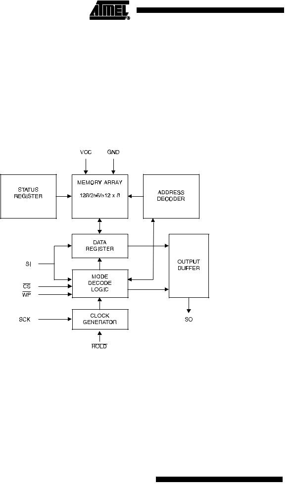
Block Diagram
2 AT25010A/020A/040A [Preliminary]
3402A–SEEPR–10/3/03

AT25010A/020A/040A [Preliminary]
Pin Capacitance(1)
Applicable over recommended operating range from TA = 25°C, f = 1.0 MHz, VCC = +5.0V (unless otherwise noted).
Symbol |
|
Test Conditions |
Max |
Units |
Conditions |
||||||
|
|
|
|
|
|
||||||
COUT |
|
Output Capacitance (SO) |
8 |
pF |
VOUT = 0V |
||||||
CIN |
|
Input Capacitance |
|
SCK, SI, |
|
|
|
|
6 |
pF |
VIN = 0V |
(CS, |
WP, |
HOLD) |
|||||||||
Note: 1. |
This parameter is characterized and is not 100% tested. |
|
|
|
|||||||
DC Characteristics
Applicable over recommended operating range from: TA = -40°C to +125°C, VCC = +2.7V to +5.5V.
Symbol |
|
Parameter |
Test Condition |
Min |
Max |
Units |
||||||
|
|
|
|
|
|
|
|
|
|
|
|
|
VCC1 |
|
Supply Voltage |
|
|
|
|
|
|
|
2.7 |
5.5 |
V |
VCC2 |
|
Supply Voltage |
|
|
|
|
|
|
|
4.5 |
5.5 |
V |
ICC1 |
|
Supply Current |
VCC = 5.0V at 1 MHz, SO = Open, Read |
|
3.0 |
mA |
||||||
ICC2 |
|
Supply Current |
VCC = 5.0V at 2 MHz, SO = Open, |
|
6.0 |
mA |
||||||
|
Read, Write |
|
|
|
|
|
|
|||||
|
|
|
|
|
|
|
|
|
|
|
||
|
|
|
|
|
|
|
|
|
|
|
|
|
ISB1 |
|
Standby Current |
VCC = 2.7V |
|
|
|
|
= VCC |
|
5 |
µA |
|
CS |
|
|||||||||||
ISB2 |
|
Standby Current |
VCC = 5.0V |
|
|
|
|
= VCC |
|
10 |
µA |
|
|
|
CS |
|
|||||||||
IIL |
|
Input Leakage |
VIN = 0V to VCC |
-0.6 |
3.0 |
µA |
||||||
IOL |
|
Output Leakage |
VIN = 0V to VCC |
-0.6 |
3.0 |
µA |
||||||
VIL(2) |
|
Input Low Voltage |
|
|
|
|
|
|
|
-0.6 |
VCC x 0.3 |
V |
VIH(2) |
|
Input High Voltage |
|
|
|
|
|
|
|
VCC x 0.7 |
VCC + 0.5 |
V |
VOL1 |
|
Output Low Voltage |
4.5V ≤ |
VCC ≤ |
5.5V |
|
|
IOL = 2.0 mA |
|
0.4 |
V |
|
VOH1 |
|
Output High Voltage |
|
IOH = -1.0 mA |
VCC - 0.8 |
|
V |
|||||
|
|
|
|
|
|
|||||||
VOL2 |
|
Output Low Voltage |
2.7V ≤ |
VCC ≤ |
5.5V |
|
|
IOL = 0.15 mA |
|
0.2 |
V |
|
VOH2 |
|
Output High Voltage |
|
IOH = -100 µA |
VCC - 0.2 |
|
V |
|||||
|
|
|
|
|
|
|||||||
Notes: 1. |
This parameter is preliminary and Atmel may change the specifications upon further characterization. |
|
||||||||||
2. VIL min and VIH max are reference only and are not tested.
3
3402A–SEEPR–10/3/03

AC Characteristics
Applicable over recommended operating range from TA = -40°C to +125°C, VCC = As Specified, CL = 1 TTL Gate and 100 pF (unless otherwise noted).
Symbol |
|
Parameter |
Voltage |
Min |
Max |
Units |
||
|
|
|
|
|
|
|
|
|
fSCK |
|
SCK Clock Frequency |
4.5 - 5.5 |
0 |
3.0 |
MHz |
||
|
2.7 - 5.5 |
0 |
1.5 |
|||||
|
|
|
|
|
|
|||
|
|
|
|
|
|
|
|
|
tRI |
|
Input Rise Time |
4.5 - 5.5 |
|
2 |
s |
||
|
2.7 - 5.5 |
|
2 |
|||||
|
|
|
|
|
|
|
||
|
|
|
|
|
|
|
|
|
tFI |
|
Input Fall Time |
4.5 - 5.5 |
|
2 |
s |
||
|
2.7 - 5.5 |
|
2 |
|||||
|
|
|
|
|
|
|
||
|
|
|
|
|
|
|
|
|
tWH |
|
SCK High Time |
4.5 - 5.5 |
133 |
|
ns |
||
|
2.7 - 5.5 |
266 |
|
|||||
|
|
|
|
|
|
|
||
|
|
|
|
|
|
|
|
|
tWL |
|
SCK Low Time |
4.5 - 5.5 |
133 |
|
ns |
||
|
2.7 - 5.5 |
266 |
|
|||||
|
|
|
|
|
|
|
||
|
|
|
|
|
|
|
|
|
tCS |
|
|
|
|
4.5 - 5.5 |
250 |
|
|
|
CS High Time |
|
ns |
|||||
|
2.7 - 5.5 |
250 |
|
|||||
|
|
|
|
|
|
|
||
|
|
|
|
|
|
|
|
|
|
|
|
|
|
4.5 - 5.5 |
250 |
|
|
tCSS |
|
CS Setup Time |
|
ns |
||||
|
2.7 - 5.5 |
250 |
|
|||||
|
|
|
|
|
|
|
||
|
|
|
|
|
|
|
|
|
|
|
|
|
|
4.5 - 5.5 |
250 |
|
|
tCSH |
|
CS Hold0 Time |
|
ns |
||||
|
2.7 - 5.5 |
250 |
|
|||||
|
|
|
|
|
|
|
||
|
|
|
|
|
|
|
|
|
tSU |
|
Data In Setup Time |
4.5 - 5.5 |
50 |
|
ns |
||
|
2.7 - 5.5 |
50 |
|
|||||
|
|
|
|
|
|
|
||
|
|
|
|
|
|
|
|
|
tH |
|
Data In Hold Time |
4.5 - 5.5 |
50 |
|
ns |
||
|
2.7 - 5.5 |
100 |
|
|||||
|
|
|
|
|
|
|
||
|
|
|
|
|
|
|
|
|
|
|
|
|
|
4.5 - 5.5 |
100 |
|
|
tHD |
|
Hold Setup Time |
|
ns |
||||
|
2.7 - 5.5 |
100 |
|
|||||
|
|
|
|
|
|
|
||
|
|
|
|
|
|
|
|
|
tCD |
|
|
|
|
4.5 - 5.5 |
200 |
|
|
|
Hold Hold Time |
|
ns |
|||||
|
2.7 - 5.5 |
200 |
|
|||||
|
|
|
|
|
|
|
||
|
|
|
|
|
|
|
|
|
tV |
|
Output Valid |
4.5 - 5.5 |
0 |
133 |
ns |
||
|
2.7 - 5.5 |
0 |
266 |
|||||
|
|
|
|
|
|
|||
|
|
|
|
|
|
|
|
|
tHO |
|
Output Hold Time |
4.5 - 5.5 |
0 |
|
ns |
||
|
2.7 - 5.5 |
0 |
|
|||||
|
|
|
|
|
|
|
||
|
|
|
|
|
|
|
|
|
tLZ |
|
|
|
|
4.5 - 5.5 |
0 |
100 |
|
|
Hold to Output Low Z |
ns |
||||||
|
2.7 - 5.5 |
0 |
100 |
|||||
|
|
|
|
|
|
|||
|
|
|
|
|
|
|
|
|
|
|
|
|
|
4.5 - 5.5 |
|
100 |
|
tHZ |
|
Hold to Output High Z |
|
ns |
||||
|
2.7 - 5.5 |
|
100 |
|||||
|
|
|
|
|
|
|
||
|
|
|
|
|
|
|
|
|
tDIS |
|
Output Disable Time |
4.5 - 5.5 |
|
250 |
ns |
||
|
2.7 - 5.5 |
|
500 |
|||||
|
|
|
|
|
|
|
||
|
|
|
|
|
|
|
|
|
tWC |
|
Write Cycle Time |
4.5 - 5.5 |
|
5 |
ms |
||
|
2.7 - 5.5 |
|
10 |
|||||
|
|
|
|
|
|
|
||
|
|
|
|
|
|
|
||
Endurance(1) |
|
5.0V, 25°C, Page Mode |
|
1M |
|
Write Cycles |
||
Note: 1. This parameter is characterized and is not 100% tested.
4 AT25010A/020A/040A [Preliminary]
3402A–SEEPR–10/3/03

Serial Interface
Description
3402A–SEEPR–10/3/03
AT25010A/020A/040A [Preliminary]
MASTER: The device that generates the serial clock.
S L A V E : B e c a u s e t h e S e r ia l C lo c k p in ( S C K ) i s a l w a y s a n i n p u t , th e AT25010A/020A/040A always operates as a slave.
TRANSMITTER/RECEIVER: The AT25010A/020A/040A has separate pins designated for data transmission (SO) and reception (SI).
MSB: The Most Significant Bit (MSB) is the first bit transmitted and received.
SERIAL OP-CODE: After the device is selected with CS going low, the first byte will be received. This byte contains the op-code that defines the operations to be performed. The op-code also contains address bit A8 in both the READ and WRITE instructions.
INVALID OP-CODE: If an invalid op-code is received, no data will be shifted into the AT25010A/020A/040A, and the serial output pin (SO) will remain in a high impedance state until the falling edge of CS is detected again. This will reinitialize the serial communication.
CHIP SELECT: The AT25010A/020A/040A is selected when the CS pin is low. When the device is not selected, data will not be accepted via the SI pin, and the serial output pin (SO) will remain in a high impedance state.
HOLD: The HOLD pin is used in conjunction with the CS pin to select the AT25010A/020A/040A. When the device is selected and a serial sequence is underway, HOLD can be used to pause the serial communication with the master device without resetting the serial sequence. To pause, the HOLD pin must be brought low while the SCK pin is low. To resume serial communication, the HOLD pin is brought high while the SCK pin is low (SCK may still toggle during HOLD). Inputs to the SI pin will be ignored while the SO pin is in the high impedance state.
WRITE PROTECT: The write protect pin (WP) will allow normal read/write operations when held high. When the WP pin is brought low, all write operations are inhibited.
WP going low while CS is still low will interrupt a write to the AT25010A/020A/040A. If the internal write cycle has already been initiated, WP going low will have no effect on any write operation.
5