


P R E L I M I N A R Y
write enables and a nonmultiplexed address bus can reduce design costs by eliminating this external logic.
Nonmultiplexed Address Bus
on the DRAM. The correct row and column addresses are generated on these odd address pins during a DRAM access.
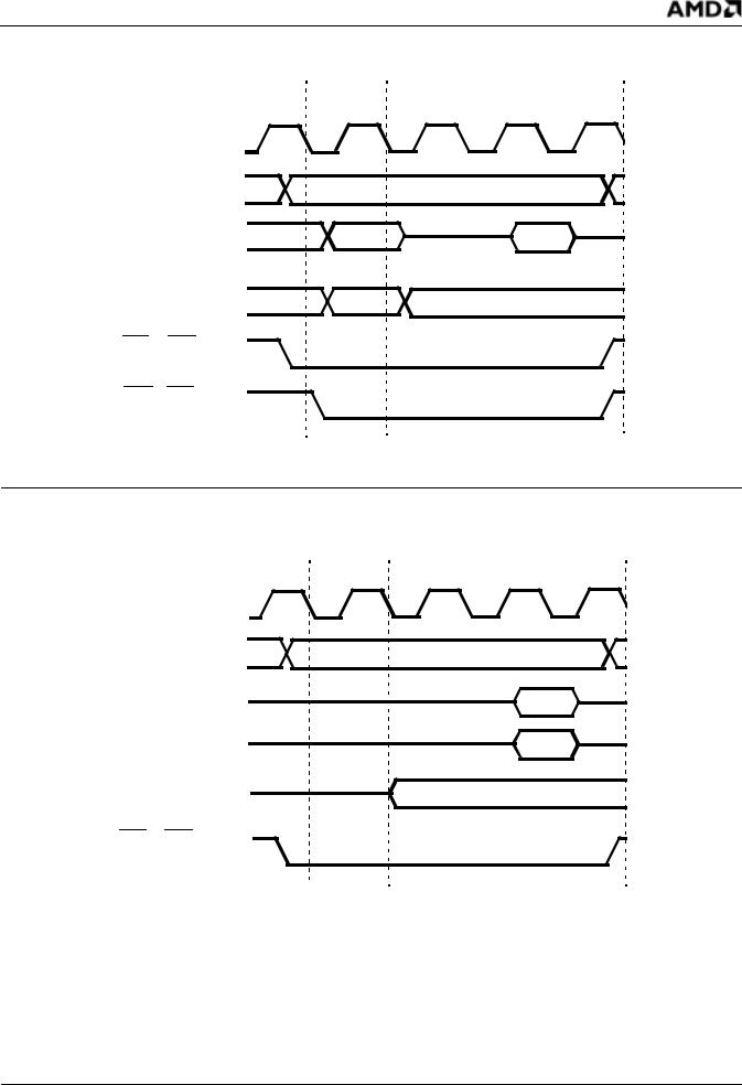
The nonmultiplexed address bus (A19–A0) is valid one-half CLKOUT cycle in advance of the address on the AD bus. When used in conjunction with the modified UCS and LCS outputs and the byte write enable signals, the A19–A0 bus provides a seamless interface to external SRAM, and Flash memory/ EPROM systems.
Byte Write Enables
The Am186CC controller provides the WHB (Write High Byte) and WLB (Write Low Byte) signals that act as byte write enables.
WHB is the logical OR of BHE and WR. WHB is Low when both BHE and WR are Low. WLB is the logical OR of A0 and WR. WLB is Low when A0 and WR are both Low.
The by te wr i te ena bl es a r e d r iv en wi th th e nonmultiplexed address bus as required for the write timing requirements of common SRAMs.
Output Enable
The Am186CC controller provides the RD (Read) signal which acts as an output enable for memory or peripheral devices.
The RD signal is Low when a word or byte is read by the Am186CC controller.
DRAM Support
To support DRAM, the Am186CC controller has a fully integrated DRAM controller that provides a glueless interface to 25–70-ns Extended Data Out (EDO) DRAM (EDO DRAM is sometimes called Hyper-Page Mode DRAM). Up to two banks of 4-Mbit (256 Kbit x 16 bit) DRAM can be accessed. Page Mode DRAM, Fast Page Mode DRAM, Asymmetrical DRAM, and 8-bit wide DRAM are not supported. The Am186CC controller includes a glueless DRAM interface providing zero-wait state operation at up to 50 MHz with 40-ns DRAM. This allows designs requiring larger amounts of memory to save system cost over SRAM designs by taking advantage of low DRAM memory costs.
The DRAM interface uses various chip select pins to implement the RAS/CAS interface required by DRAMs. The Am186CC DRAM controller drives the RAS/CAS interface appropriately during both normal memory accesses and during refresh. All signals required are generated by the Am186CC controller and no external logic is required.
The DRAM multiplexed address pins are connected to the Am186CC controller’s odd address pins, starting with A1 on the Am186CC controller connecting to MA0
The RAS pins are multiplexed with LCS and MCS3, allowing a DRAM bank to be present in either high or low memory space. The MCS2 and MCS1 function as the upper and lower CAS pins, respectively, and define which byte of data in a 16-bit DRAM is being accessed.
The Am186CC controller supports the most common DRAM refresh option, CAS-Before-RAS. All refresh cycles contain three wait states to support the DRAMs at various frequencies. The DRAM controller never performs a burst access. All accesses are single accesses to DRAM. If the PCS chip selects are decoded to be in the DRAM address range, PCS accesses take precedence over the DRAM.
Chip Selects
The Am186CC controller provides six chip select outputs for use with memory devices and eight more for use with peripherals in either memory or I/O space. The six memory chip selects can be used to address three memory ranges. Each peripheral chip select a dd r e s s e s a 2 5 6 - by t e b l oc k o ffs e t f r om a programmable base address.
The Am186CC controller can be programmed to sense a ready signal for each of the peripheral or memory chip select lines. A bit in each chip select control register determines whether the external ready signal is required or ignored.
The chip selects can control the number of wait states inserted in the bus cycle. Although most memory and peripheral devices can be accessed with three or less wait states, some slower devices cannot. This feature allows devices to use wait states to slow down the bus.
The chip select lines are active for all memory and I/O cycles in their programmed areas, whether they are generated by the CPU or by the integrated DMA unit.
General enhancements over the original 80C186 include bus mastering (three-state) support for all chip selects and activation only when the associated register is written, not when it is read.
Clock Control
The processor supports clock rates from 25 to 50 MHz. Commercial and industrial temperature ratings are available. Separate crystal oscillator inputs are provided for the USB and CPU. Flexibility is provided to run the entire device from a 12-, or 24-MHz crystal when the USB is in use. The CPU can run in 1x, 2x, or 4x mode; USB can run in 2x or 4x mode.
32 |
Am186™CC Communications Controller Data Sheet |
|
P R E L I M I N A R Y |
|
|
|
|
t1 |
t2 |
t3 |
t4 |
|
Address |
|
Data |
|
|
Phase |
|
Phase |
|
CLKOUT |
|
|
|
|
A19–A0 |
|
Address |
|
|
AD15–AD0 |
Address |
|
Data |
|
(Read) |
|
|
||
|
|
|
|
|
AD15–AD0 |
Address |
|
Data |
|
(Write) |
|
|
||
|
|
|
|
|
LCS or UCS |
|
|
|
|
MCSx, PCSx |
|
|
|
|
Figure 3. Am186CC Controller Address Bus — Default Operation
t1 |
t2 |
t3 |
t4 |
Address |
|
Data |
|
Phase |
|
Phase |
|
CLKOUT |
|
|
|
A19–A0 |
|
Address |
|
AD7–AD0 |
|
Data |
|
(Read) |
|
|
|
AD15–AD8 |
|
Data |
|
(Read) |
|
|
|
AD15–AD0 |
|
Data |
|
(Write) |
|
|
|
LCS or UCS |
|
|
|
Figure 4. Am186CC Controller—Address Bus Disable In Effect
Am186™CC Communications Controller Data Sheet |
33 |

P R E L I M I N A R Y
In-Circuit Emulator Support
Because pins are an expensive resource, many play a dual role, and the programmer selects PIO operation or an alternate function. However, a pin configured to be a PIO may also be required for emulation support. Therefore, it is important that before a design is committed to hardware, a user should contact potential emulator suppliers for a list of their emulator’s pin requirements.
The Am186CC controller was designed to minimize conflicts. In most cases, pin conflict is avoided. For example, if the ALE signal is required for multiplex bus support, then it would not be programmed as PIO33. If the multiplexed AD bus is not used, then ALE can be programmed as a PIO pin. If the multiplexed bus is not in use, then the emulator does not require the ALE signal.
APPLICATIONS
The Am186CC controller, with its integrated HDLC, USB, and other communications features, provides a highly integrated, cost-effective solution for a wide range of telecommunications and networking applications.
νISDN Modems and Terminal Adapters: Nextgeneration ISDN equipment requires USB (or highspeed UART capability), in addition to three channels of HDLC.
νLow-End Routers: ISDN to Ethernet-based personal routers, often used for connections in Small Office/Home Office (SOHO) environments, require three channels of HDLC, as well as the high performance of a 16-bit controller.
νLinecard Applications: Typically, linecards used in Central Offices (COs), PABX equipment, and other telephony applications require one or two channels of HDLC. Linecard manufacturers are moving to more lines per card for analog POTS as a means of cost reduction. This, and digital linecards for support of ISDN, often require higher performance than existing 8-bit devices can offer. The Am186CC controller is an ideal solution for these applications because it integrates much of the necessary glue logic while providing higher performance.
νxDSL Applications: Today’s xDSL applications, such as high-speed ADSL modems, require data handling of 2 Mbit/s or greater and can take advantage of the USB interface for easy connectivity to the PC.
νDigital Corded Phones: Typical digital telephone applications use up to three channels of HDLC and may use USB for merged PC telephony applications.
νIndustrial Control: Embedded x86 processors have long been used in the industrial control market. These applications often require a robust, highperformance processor solution with one or two channels of HDLC.
νUSB Peripheral Devices: These devices will become more common as the PC market embraces the USB protocol specified by Microsoft’s Windows 98 operating system. In addition to implementing communications device class systems such as an ISDN terminal adapter, the USB controller makes the Am186CC controller suitable for certain PC desktop applications such as a USB camera interface, ink-jet printers, and scanners.
νGeneral Communications Applications: The Am186CC controller will also find a home in general embedded applications, because many devices will incorporate communications capability in the future. Many designs are adding HDLC capability as a robust means of interand intra-system communications. The Am186CC controller is especially attractive for 186 designs adding HDCL, USB, or both.
Block diagrams on the following pages show some typical Am186CC controller designs: Figure 5 on page 35 shows an ISDN terminal adapter system application, Figure 6 on page 35 shows an ISDN to Ethernet low-end router application, and Figure 7 on page 36 shows a 32-channel linecard application.
The ISDN terminal adapter features an S/T or U interface and either a high-speed UART or USB connection for attaching the modem to the PC.
The ISDN-to-Ethernet low-end router features an S/T or U interface, two POTS lines, and a 10-Mbit/s connection to the PC.
The 32-channel linecard design demonstrates the Am186CC controller’s use in a linecard application where 32 lines terminate on the linecard.
34 |
Am186™CC Communications Controller Data Sheet |

P R E L I M I N A R Y
I
Figure 5. ISDN Terminal Adapter System Application
Figure 6. ISDN to Ethernet Low-End Router System Application
Am186™CC Communications Controller Data Sheet |
35 |

P R E L I M I N A R Y
Figure 7. 32-Channel Linecard System Application
36 |
Am186™CC Communications Controller Data Sheet |