


P R E L I M I N A R Y
|
System Operating Frequency |
|
|
|
|
|
|
|
|||||
|
0 MHz |
|
|
20 MHz 24 MHz |
30 MHz |
|
40 MHz |
50 MHz |
|||||
|
|
|
|
|
|
|
|
|
|
|
|
|
|
|
|
16 MHz |
|
|
|
|
|
|
32 MHz |
|
|
|
|
|
|
|
|
|
|
|
|
|
|
|
|||
|
|
|
|
|
|
|
|||||||
|
|
|
|
|
|
|
|
|
|
|
|
|
|
4x Mode |
|
|
|
|
|
|
|
|
8-MHz to 12.5-MHz Xtal or Clock |
|
|
||
|
|
|
|
|
|
|
|
|
|||||
|
|
|
|
|
|
|
|
|
|
|
|
|
|
|
|
|
|
|
|
|
|
|
|
|
|
|
|
|
|
|
|
|
|
|
|
|
|
|
|
|
|
|
|
|
|
|
|
|
|
|
|
|
|
|
|
|
|
|
|
|
|
|
|
|
|
|
|
|
|
|
|
|
|
|
|
|
|
|
|
|
|
|
|
2x Mode |
|
|
8-MHz to 25-MHz Xtal or Clock |
|
|
||
|
|||
|
|
|
|
|
|
|
|
|
|
|
|
|
|
|
|
|
|
|
|
|
|
|
|
|
|
|
|
|
|
|
|
|
|
|
|
|
|
|
|
|
|
|
|
|
|
|
|
|
|
|
|
|
1x Mode |
|
|
16-MHz to 40-MHz Xtal or Clock1 |
|
|
|||
|
|
|
|
|
|
|
|
|
PLL
Bypass 0-MHz to 24-MHz Xtal or Clock
Mode
PLL Bypass Mode |
|
1x Mode |
|
2x Mode |
|
4x Mode |
|
|
|
|
|
|
|
1The crystal oscillator is not guaranteed above 40 MHz.
Figure 9. Suggested System Clock Frequencies, Clock Modes and Crystal Frequencies
Crystal-Driven Clock Source
The internal oscillator circuit is designed to function with an external parallel-resonant fundamental mode crystal. The crystal frequency can vary from 8 to 40 MHz, depending on the PLL mode selected and desired system frequency.
Selecting a Crystal
When selecting a crystal, the load capacitance should always be specified (CL). This value can cause variance in the oscillation frequency from the desired specified value (resonance). The load capacitance and the loading of the feedback network have the following relationship:
CL = ((C1 +× C2)) + CS
C1 C2
where CS is the stray capacitance of the circuit.
Table 6 shows crystal parameter values. Figure 10 shows the system clocks using an external crystal and the integrated oscillator. The specific values for C1 and C2 must be determined by the designer and are dependent on the characteristics of the chosen crystal and board design.
Table 6. |
Crystal Parameters |
|||
|
|
|
|
|
Parameter |
|
Min. |
Max. |
Units |
|
Value |
Value |
||
|
|
|
||
|
|
|
|
|
Frequency |
|
8 |
40 |
MHz |
|
|
|
|
|
ESR |
|
20 |
60 |
ohms |
|
|
|
|
|
Load capacitance |
|
10 |
TBD |
pF |
|
|
|
|
|
Mode |
|
|
|
Fundamental |
|
|
|
|
|
Frequency tolerance |
|
TBD |
TBD |
ppm |
|
|
|
|
|
Drive level |
|
|
500 |
mW |
|
|
|
|
|
|
X1 |
|
Xtal |
|
X2 |
C1 |
C2 |
Figure 10. External Interface to Support Clocks— Fundamental Mode Crystal
Am186™CC Communications Controller Data Sheet |
39 |
P R E L I M I N A R Y
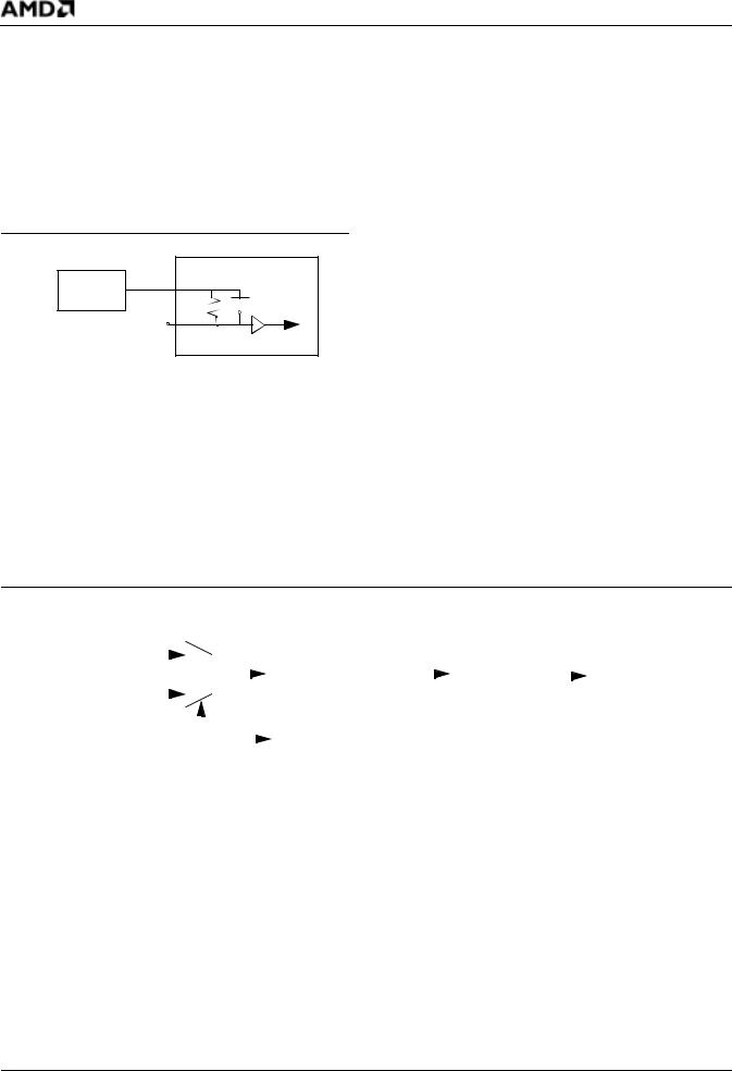
External Clock Source
The internal oscillator also can be driven by an external clock source. The external clock source should be connected to the input of the inverting amplifier (X1 or US BX1) with the output ( X2 or USBX2) left unconnected. Figure 11 shows the system clocks using an external clock source (oscillator bypass).
Note: X1, X2, USBX1, and USBX2 are not 5-V tolerant and have a maximum input equal to VCC.
Static Operation
The Am186CC controller is a fully static design and can be placed in static mode by stopping the input clock. PLL bypass mode must be used with an external clock source.
Note: It is the responsibility of the system designer to ensure that no short clock phases are generated when starting or stopping the clock.
UART Baud Clock
External |
|
X1/USBX1 |
Clock |
|
|
|
NC |
X2/USBX2 |
|
|
Figure 11. External Interface to Support Clocks— External Clock Source
The UARTs (lowand high-speed) have two possible clock sources: the system clock or the UCLK input pin. If UCLK is used for the UART clock, the system clock must be at least the same frequency as UCLK. The clock configurations are shown graphically in Figure 12.
The baud clock is generated by dividing the clock source by the value of baud rate divisor register. The serial port logic can select its baud rate clock from either an external pin (UCLK) or from the CPU clock.
The CPU or UCLK clock is selected independent of any other settings.
The formula for determining the baud rate divisor register value is:
BAUDDIV = (clock frequency/(16 • baud rate))
Note: UCLK cannot be clocked at a frequency higher than the system clock frequency.
System Clock |
|
|
|
|
|
|
|
|
|
|
Oversample |
|
|
|
|
|
|
|
|
|
|
|
|
|
|
|
|
|
|||
|
|
|
|
|
|
|
|
|
Baud |
Clock |
Divide for |
|
|
||
|
|
|
|
|
|
|
|
|
|
|
|
||||
|
|
|
|
|
|
|
|
|
|
|
|
|
Baud Clock |
||
UCLK |
|
|
|
|
|
|
|
|
|
Divisor |
|
|
Oversampling |
|
|
|
|
|
|
|
|
||||||||||
UART/High-Speed UART |
|
|
|
|
|
|
|
|
|
|
|
|
|
|
|
|
|
|
|
|
|
|
|
|
|
|
|
||||
|
|
|
|
|
|
Autobaud Clock |
|
|
|
||||||
|
|
|
|
|
|
|
|
||||||||
|
|
|
|
|
|
|
|
|
|
|
|||||
Clock Select |
|
|
|
|
|
|
|
||||||||
|
|
|
|
(High-Speed UART Only) |
|
|
|
||||||||
|
|
|
|
|
|
|
|
|
|
|
|
|
|||
Figure 12. UART and High-Speed UART Clocks
40 |
Am186™CC Communications Controller Data Sheet |