

dsd1-10 / dsd-04=Ermak / DSD4 / DSD4_l5_new
.docDESIGNING COMBINATIONAL LOGIC GATES IN CMOS
Static CMOS Design
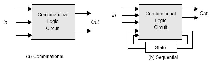
The complementary CMOS circuit style falls under a broad class of logic circuits called static circuits in which at every point in time (except during the switching transients), each gate output is connected to either VDD or Vss via a low-resistance path.
The dynamic circuit class, that relies on temporary storage of signal values on the capacitance of high-impedance circuit nodes.
Complementary CMOS
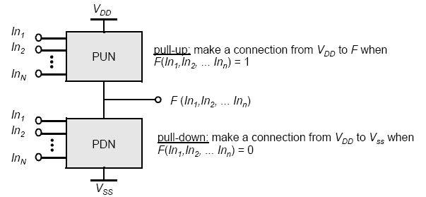
Complementary logic gate as a combination of a PUN (pull-up network) and a PDN (pull-down network).
-
The PDN is constructed using NMOS devices, while PMOS transistors are used in the PUN.
-
The NMOS transistors produce “strong zeros,” and PMOS devices generate “strong ones”.

-
The parallel connection of transistors in the pull-up network corresponds to a series connection of the corresponding devices in the pull-down network, and vice versa.
-
The complementary gate is naturally inverting, implementing only functions such as NAND, NOR, and XNOR.
-
The number of transistors required to implement an N-input logic gate is 2N.
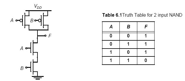
Two-input NAND gate in complementary static CMOS style.
Static Properties of Complementary CMOS Gates

Propagation Delay of Complementary CMOS Gates
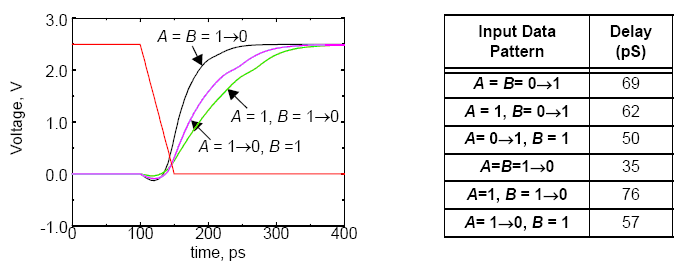
Tlh = 0.69 × (Rp/2) × C (A = B = 1 → 0)
Tlh = 0.69 × Rp × CL (A = 1, B = 1 → 0)
Thl = 0.69 × (2RN) × CL (A = B = 0 → 1)
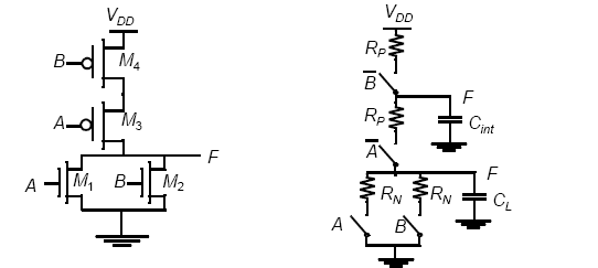
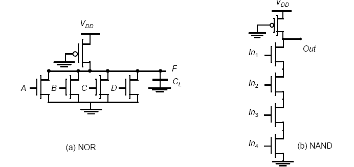
The CMOS implementation of a NOR gate (F = A + B)
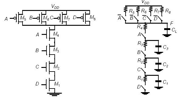
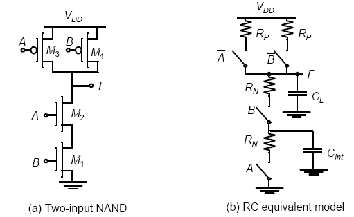
Four input NAND gate along with the internal node capacitances.
![]()
![]()
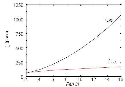
Propagation delay of CMOS NAND gate as a function of fan-in
Design Techniques for Large Fan-in
Design Techniques for Large Fan-in
-
Transistor Sizing
-
Progressive Transistor Sizing (M1 > M2 > M3 > MN)
-
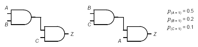
Input Re-Ordering
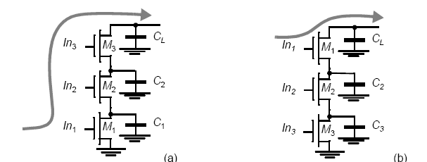
-
Logic Restructuring
Power Consumption in CMOS Logic Gates

Design Techniques to Reduce Switching Activity
-
Logic Restructuring

-
Input ordering
-
Time-multiplexing resources
-
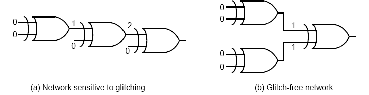
Glitch Reduction by balancing signal paths
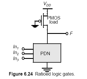
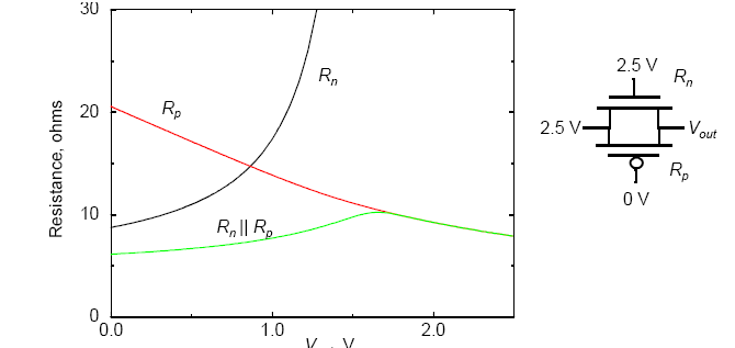
Ratioed Logic (pseudo-NMOS style)
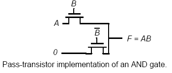
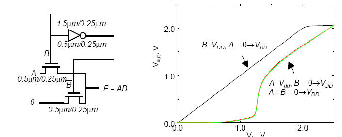
Pass-Transistor Logic
Differential Pass Transistor Logic
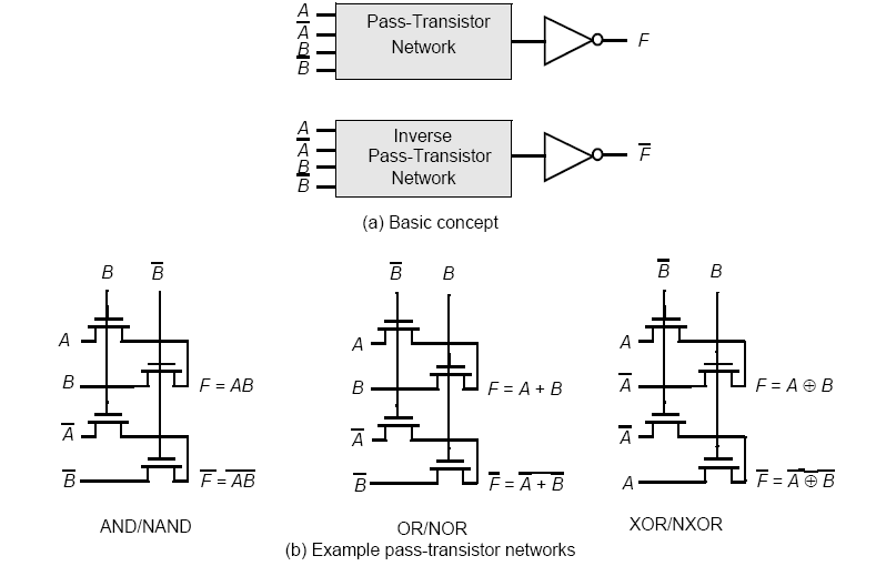
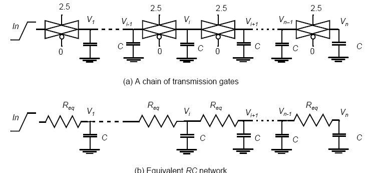
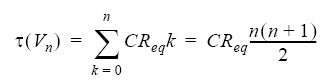
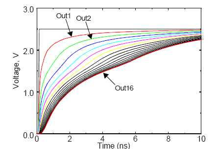
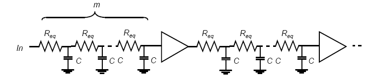
Transmission Gate Logic

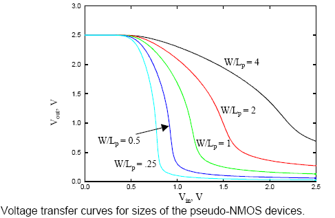
for (W/L)n = (W/L)p = 0.5um/0.25um
Dynamic CMOS Design

The operation of this circuit can be divided into two major phases: precharge and evaluation, with the mode of operation determined by the clock signal.
-
Logic function is implemented by the PDN only
-
number of transistors is N + 2 (versus 2N for static complementary CMOS)
-
should be smaller in area than static complementary CMOS
-
-
Full swing outputs (VOL = GND and VOH = VDD)
-
Nonratioed - sizing of the devices is not important for proper functioning
-
Faster switching speeds
-
reduced load capacitance due to lower number of transistors per gate (Cint)
-
reduced load capacitance due to smaller fan-out (Cext)
-
no Isc, so all the current provided by PDN goes into discharging CL
-
Properties of Dynamic Gates, con’t
-
Power dissipation should be better
-
consumes only dynamic power – no short circuit power consumption since the pull-up path is not on when evaluating
-
lower CL
-
by construction can have at most one transition per cycle – no glitching
-
But power dissipation can be significantly higher due to
-
higher transition probabilities
-
extra load on CLK
3. PDN starts to work as soon as the input signals exceed VTn, so set VM, VIH and VIL equal to VTn
-
low noise margin (NML)
4. Needs a precharge clock
Summary
In this chapter, we have extensively analyzed the behavior and performance of combinational CMOS digital circuits with regard to area, speed, and power.
• Static complementary CMOS combines dual pull-down and pull-up networks, only one of which is enabled at any time.
• The performance of a CMOS gate is a strong function of fan-in. Techniques to deal with fan-in include transistor sizing, input reordering, and partitioning. The speed is also a linear function of the fan-out. Extra buffering is needed for large fan-outs.
• The ratioed logic style consists of an active pull-down (up) network connected to a load device. This results in a substantial reduction in gate complexity at the expense of static power consumption and an asymmetrical response. Careful transistor sizing is necessary to maintain sufficient noise margins. The most popular approaches in this class are the pseudo-NMOS techniques and the differential DCVSL, which requires complementary signals.
• Pass-transistor logic implements a logic gate as a simple switch network. This results in very simple implementations for some logic functions. Long cascades of switches are to be avoided due to a quadratic increase in delay with respect to the number of elements in the chain. NMOS-only pass-transistor logic produces even simpler structures, but might suffer from static power consumption and reduced noise margins. This problem can be add ressed by adding a level-restoring transistor.
• The operation of dynamic logic is based on the storage of charge on a capacitive node and the conditional discharging of that node as a function of the inputs. This calls for a two-phase scheme, consisting of a precharge followed by an evaluation step. Dynamic logic trades off noise margin for performance. It is sensitive to parasitic effects such as leakage, charge redistribution, and clock feedthrough. Cascading dynamic gates can cause hazards and should be addressed carefully.
• The power consumption of a logic network is strongly related to the switching activity of the network. This activity is a function of the input statistics, the network topology, and the logic style.
• Sources of power consumption such as glitches and short-circuit currents can be minimized by careful circuit design and transistor sizing.
• Power consumption is minimized by reducing the supply voltage, which increases the delay. Trading off area for power is a way to compensate for that performance loss.