

- •Contents
- •Preface
- •Related Documents
- •Typographic and Syntax Conventions
- •Getting Started
- •Starting the Schematic Composer
- •Using the Command Interpreter Window
- •Working with Designs
- •Opening a New Cellview
- •Opening an Existing Cellview
- •Using the Schematic Editor
- •Using the Symbol Editor
- •Making Designs Editable
- •Making Designs Read Only
- •Saving Your Edits
- •Closing Editor Windows
- •Quitting the Schematic Composer
- •Working with Libraries
- •Database Structure
- •Design Libraries
- •Reference Libraries
- •Library Browser
- •Using Menus and the Icon Bar
- •Using Pull-Down Menus
- •Using Pop-Up Menus
- •Using Object-Sensitive Menus (OSMs)
- •Using the Icon Bar
- •Working with Commands
- •Using Command Prompts
- •Canceling a Command
- •Undoing a Command
- •Redoing a Command
- •Displaying a Form
- •Using Form Buttons
- •Using Form Fields
- •Quick Reference Bindkey Charts
- •Quick Reference Bindkey Chart — Schematic Editor
- •Quick Reference Bindkey Chart — Symbol Editor
- •Quick Reference Bindkey Chart — Mouse Buttons
- •Quick Reference Bindkey Chart — General Bindkeys
- •Selecting Objects
- •Dynamic Highlighting
- •Using the Mouse to Select Objects
- •Extending the Selection Area of a Net
- •Selecting One Object
- •Selecting Multiple Objects
- •Selecting Parts of Objects
- •Selecting Wires
- •Selecting a Wire Name and Its Associated Wire Segments
- •Selecting a Pin and Its Associated Wire Segments
- •Selecting an Instance and Its Associated Wire Segments
- •Deselecting Objects
- •Working with Windows
- •Zooming
- •Panning
- •Redrawing a Window
- •Viewing the Same Cell in Two Windows
- •Saving View Area Settings in Memory
- •Restoring View Area Settings
- •Using the Library Browser
- •Accessing and Using the Library Browser
- •Changing the Browser Type Option
- •Using the Library Browser to Initialize Form Fields
- •Using the Component Browser
- •Accessing and Using the Component Browser
- •Changing the Browser Type Option to the Component Browser
- •Opening the Component Browser
- •Opening the Add Instance Form Instead of the Component Browser
- •Listing Components from Several Libraries
- •Changing the Component Browser Display
- •Connectivity with Objects
- •Instance Naming Conventions
- •System-Generated Names
- •Iterated Names
- •Wire Connections and Wire Naming Conventions
- •Wire-to-Wire Connections
- •Wire-to-Pin Connections
- •Wire-by-Name Connections
- •Wire-to-Iterated Instance Connections
- •Global Net Name Connections
- •Multiple-Bit Wire Connections
- •Tapping Multiple Bits of a Bundle
- •Tapping Multiple Bits of a Bus
- •Tapping Wire Intersections by Name
- •Designating Tap Size and Bit Order
- •System-Generated Net Names
- •Multiple-Bit Wire Naming Conventions
- •Using Vector Expressions in Multiple Signals
- •Evaluating Vector Expressions in Multiple-Bit Wire Names
- •Pin Connections and Pin Naming Conventions
- •Hierarchical Pin Names
- •Offsheet Pin Names
- •Bus Pin Names
- •Pin-to-Pin Connections
- •Tapping Pins
- •Naming Single and Multiple Bits Using Patchcords
- •Naming Multiple Nets Using Patchcords
- •Inherited Connections
- •Inherited Connections in a Hierarchy
- •The Syntax of an Inherited Net Expression
- •How Net Expressions Evaluate
- •Sample Net Expression Library
- •Inherited Connections Restrictions
- •Analyzing Net Expression Property Names and Evaluated Names
- •Summary of Naming Conventions
- •Creating Schematics
- •Getting Started with Schematics
- •Adding Instances
- •What Is an Instance?
- •Methods of Adding an Instance to Your Design
- •Adding Instances One by One
- •Adding Instances by Rows and Columns (an Array)
- •Adding Instances Using an Iterative Expression
- •Editing Instance Masters
- •Specifying the View to Use While Placing the Instance
- •Changing the View after an Instance Is Already Placed
- •Renumbering Instances
- •Adding Blocks
- •Adding Blocks
- •Adding Wires and Pins to Blocks
- •Changing the Block Pin Direction Rule
- •Changing the Direction or Name of a Single Block Pin
- •Changing the Names and Directions of Multiple Block Pins
- •Deleting Block Pins
- •Disabling Automatic Block Pin Creation
- •Adding Pins
- •Adding Schematic and Offsheet Pins
- •Showing Pin Connections
- •Adding Wires
- •Adding Narrow or Wide Wires
- •Using Wire Snap and Gravity Options
- •Using Wire Draw, Width, and Route Options
- •Using Wire Flight Lines Option
- •Routing Flight Lines
- •Manipulating Wires with Only the Mouse
- •Adding Wires to Schematic Instance Pins using SKILL
- •Adding Wire Names
- •Naming a Wire
- •Adding Wire Names
- •Adding Multiple Wire Names
- •Verifying Invisible Wire Names
- •Adding Net Expression Labels to Create an Inherited Connection
- •Adding a Net Expression Label to a Wire
- •Adding an Inherited Supply Symbol to a Wire
- •Editing a Net Expression Label
- •Changing the Net Expression Label Display
- •Deleting a Net Expression Label
- •Adding netSet Properties to Create an Inherited Connection
- •Adding a netSet Property to an Instance
- •Modifying a netSet Property
- •Deleting a netSet Property
- •Finding a Net Expression
- •Finding and Replacing a Net Expression
- •Finding Available Properties
- •Viewing the Evaluated Net Names
- •Viewing the Full List of all Hierarchical Paths
- •Checking the Net Expression
- •Adding Solder Dots
- •Adding Solder Dots
- •Deleting Solder Dots
- •Disabling Automatic Solder Dot Creation
- •Changing Solder Dot Size
- •Adding Notes
- •Adding Note Shapes
- •Adding Note Text
- •Importing an ASCII File for Note Text
- •Adding Patchcords
- •Adding Probes
- •Adding Probes to a Net, Pin, or Instance
- •Showing Probe Information
- •Removing Probes from a Net, Pin, or Instance
- •Removing All Probes
- •Saving Probes
- •Loading Probes
- •Creating a Multisheet Schematic
- •Browsing a List of Multisheets
- •Converting a Single-Sheet Schematic to a Multisheet Schematic
- •Adding New Sheets
- •Editing the Title Block
- •Editing the Sheet Border Size and Type
- •Adding Offsheet Pins to Multisheet Schematics
- •Understanding the Index Schematic
- •Going to and from the Index Schematic
- •Repositioning a Schematic within the Sheet Borders
- •Deleting Sheets
- •Reordering Sheets
- •Renumbering Sheets
- •Working with Cross-References
- •Understanding Cross-Reference Zones
- •Understanding Pin Cross-References
- •Understanding Cross-Reference Reports
- •Preparing to Cross-Reference
- •Displaying Cross-References
- •Zooming In to View All Cross-Referenced Pins One by One
- •Viewing Cross-Reference Reports
- •Editing a Cross-Reference Display
- •Controlling the Format String Syntax
- •Customizing the Format String Syntax
- •Customizing Multisheets
- •The Basic Procedure
- •Customizing the Types and Sizes of Sheet Borders
- •Customizing the Cross Reference Options Form
- •Drawing a Customized Sheet Border
- •Drawing a Sheet Border
- •Drawing Sheet Zones
- •Drawing Zone Labels
- •Adding the Sheet Zone Property
- •Adding a Title Block
- •Adding Title Block Values with Normal Labels
- •Adding Title Block Values with NLP and IL Labels
- •Verifying the Label Type
- •Adding Title Block Properties
- •Customizing Pin Cross-References
- •Presetting the Title Block Values
- •Creating Symbols
- •Setting Grid Options
- •Importing Symbols
- •Creating New Symbols
- •Drawing Lines
- •Drawing Rectangles
- •Drawing Polygons
- •Drawing Circles
- •Drawing Ellipses
- •Drawing Arcs
- •Adding Pins as Graphic Images
- •Adding Pins as Instances
- •Creating Custom Pins as Graphic Images
- •Duplicating Pin Figures in the Symbol Master
- •Making the Custom Pin Name Visible
- •Adding a Selection Box
- •Adding Labels
- •Adding a Normal Label
- •Adding an NLP Label
- •Adding an IL Label
- •Adding Note Text and Note Shapes
- •Adding a Net Expression Label
- •Setting the Symbol Origin
- •Creating Symbol Cellviews Using Generators
- •Automatically Creating Cellviews
- •Features of Creating Cellviews
- •Automatically Creating a Cellview from Another Cellview
- •Replacing an Existing Symbol Cellview
- •Modifying an Existing Symbol Cellview
- •Examples of Replacing and Modifying Pins on a Symbol
- •Automatically Creating a Cellview from a Pin List
- •Automatically Creating a Cellview from an Instance
- •Editing Symbol Generation Options
- •Adding, Changing, and Reordering Pin Names
- •Editing Pin Attributes
- •Loading and Saving a TSG Template File
- •Editing Symbol Attributes
- •Editing Symbol Labels
- •Creating a New Label
- •Deleting Labels
- •Modifying Label Attributes
- •Editing Properties
- •Creating a New Property
- •Deleting Properties
- •Modifying Property Attributes
- •Specifying Symbol Generator Pin Sorting
- •Editing Objects
- •Using Direct Manipulation
- •Direct Manipulation Operations
- •Turning Off Direct Manipulation
- •Undoing and Redoing an Edit
- •Changing the Undo Limit
- •Stretching
- •Stretching with the Schematic Editor
- •Stretching with the Symbol Editor
- •Stretching with Direct Manipulation
- •Stretching with Bindkeys
- •Copying
- •Copying Single Objects
- •Copying Arrays of Objects
- •Copying Across Cellviews
- •Copying with Direct Manipulation
- •Copying with Bindkeys
- •Moving
- •Moving Objects
- •Moving with Direct Manipulation
- •Moving with Bindkeys
- •Deleting
- •Deleting Preselected Objects
- •Deleting Postselected Objects
- •Deleting Sheet Borders
- •Rotating
- •Rotating Preselected Objects
- •Rotating Postselected Objects
- •Rotating with Direct Manipulation
- •Rotating with Bindkeys
- •Discarding Edits
- •Alternating Symbol Views
- •Changing the View of a Preselected Object
- •Changing the View of a Postselected Object
- •Toggling Objects
- •Toggling Pin Direction Options
- •Toggling Wire Draw Mode Options
- •Toggling Instance Symbol View Options
- •Saving the Current Label Display File
- •Loading the Current Label Display File
- •Attaching the Label Display File to the Library
- •Detaching the Label Display File from the Library
- •Setting the Simulation Data Directory
- •Editing Properties
- •Using Command Shortcuts
- •Search String Wildcards
- •Replacing Properties
- •Replacing String-Tagged Characters
- •Selecting Objects to Edit
- •Using Modal (Repeating) Commands
- •Selecting Objects by Filtering
- •Selecting Objects Automatically by Type
- •Selecting Objects by Property
- •Adding a Property Name to the Search List
- •Selecting Objects by Filtering
- •Object and Cellview Property Types and Values
- •Editing Object Properties
- •Applying Edits to Objects and Displaying Object Types
- •Adding Object Properties
- •Deleting Object Properties
- •Modifying Object Properties
- •Editing Instance and Block Properties
- •Editing Pin Properties
- •Designating the Order of Pins
- •Copying a Pin Order from Another Cellview
- •Resolving Pin Order Mismatch
- •Verifying Pin Order
- •Editing Pin Name Properties
- •Editing Wire Properties
- •Editing Wire Name Properties
- •Editing Instance Pin Properties on an Instance of a Block
- •Editing Label Properties
- •Resetting Invisible Labels
- •Editing netSet Properties
- •Editing Note Text Properties
- •Editing Note Shape Properties
- •Editing Symbol Shape Properties
- •Editing Symbol Pin Properties
- •Editing Symbol Label Properties
- •Editing Symbol Selection Box Properties
- •Passing Parameters in a Design
- •Editing Cellview Properties
- •Adding Cellview Properties
- •Deleting Cellview Properties
- •Modifying Cellview Properties
- •Editing VHDL Properties
- •Adding VHDL Properties
- •Deleting VHDL Properties
- •Modifying VHDL Properties
- •Setting the Tool Filter
- •About the Design Hierarchy
- •Exploring the Design Hierarchy
- •Top-Level Schematic View
- •Middle-Level Schematic View
- •Lower-Level Design Hierarchy
- •About the Hierarchy Editor
- •Traversing a Design Hierarchy
- •Descending Using the Descend Command
- •Editing an Instance in Place
- •Descending Using the View Name List
- •Setting the View Precedence Order
- •Returning Up the Design Hierarchy
- •Using OSMs to Traverse the Design Hierarchy
- •Using Bindkeys to Traverse the Design Hierarchy
- •Displaying the Current Hierarchical Scope
- •About the Hierarchy Editor within the Schematic Composer
- •Opening a Hierarchy Editor Menu within the Schematic Composer
- •Setting Instance Bindings
- •Building a New Inherited View List
- •Showing Views Found
- •Checking Designs
- •Features of the Check Commands
- •Setting the Check Options
- •Setting User Preferences
- •Setting Schematic Rule Checks
- •Checking a Design
- •Checking and Saving a Design
- •Checking the Current Cellview
- •Checking a Design Hierarchy
- •Checking Multisheet Schematics
- •Checking a Label Attachment
- •Cross-View Checking
- •Bypassing Checks
- •Bypassing Floating Pin Checks
- •Bypassing Unconnected Wire Checks
- •Resolving Check Errors
- •Finding Errors and Warnings in a Design
- •Mapping an Error Message to a Marker
- •Managing the Error Message List
- •Assigning an ignoreCheck Property
- •Suppressing Message Displays
- •Deleting an ignoreCheck Property
- •Deleting All ignoreCheck Properties
- •Deleting Individual Markers
- •Deleting All Markers
- •Monitoring a Verilog or VHDL Simulation State
- •Using Cross Selection
- •Opening an SHM Database
- •Displaying the Simulation State of Wires and Pins
- •Setting a Time Value for Displaying Signal Results
- •Setting the Time Scale
- •Setting the Display Radius
- •Synchronizing with Simulation at Breakpoint
- •Closing the SHM Database
- •Plotting Designs
- •Setting Up System Options to Plot
- •Setting Up Printer Options to Use Various Paper Sizes
- •Plotting a Design
- •Plotting a Library
- •Plotting a Cellview
- •Plotting Part of a Schematic
- •Plotting Without a Header Page for Every Session
- •Adding Notes to a Plot
- •Setting Plot Options
- •Plotting a Color Schematic in Black and White
- •Changing the Background Color of a Schematic Window
- •Using a Plot Template File
- •Creating a Plot Template File
- •Loading a Plot Template File
- •Creating a Default Plot Template File
- •Checking the Queue Status
- •Canceling a Plot Job
- •Setting Schematic Composer Options
- •Overview of Schematic Composer Options
- •Changing User Preferences
- •Minimizing Mouse Clicks
- •Changing the Default Display Setting for Command Option Forms
- •Saving the Current Window Setup
- •Restoring a Saved Window Setup
- •Viewing Bindkey Settings
- •Changing Browser and CIW Preferences
- •Customizing Editor Options
- •Canceling the Modal (Repeat) Command Option
- •Changing Display Options
- •Selecting Objects Using the Filter Option
- •Setting Plot Options
- •Setting Schematic Check Options and Rules
- •Setting the Tool Filter
- •Saving Form Field Default Settings
- •Loading Form Field Default Settings
- •Customizing the Schematic Composer
- •Customizing Pull-Down and Pop-Up Menus
- •Sample Menu File
- •Customizing Object-Sensitive Menus
- •Example of Customizing the Instance OSM
- •Customizing the Icon Bar
- •Positioning Icons and Turning Off Icon Names
- •Changing the Contents of the Icon Bar
- •Changing the Display of the Icon Bar
- •Understanding Initialization and Setup Files
- •Converting a Schematic from a 0.125 Grid to a 0.1 Grid
- •Customizing Bindkeys
- •Locating the schBindKeys.il Bindkey File
- •Locating Your Installation Directory
- •Loading Your Customized Bindkey File
- •Loading the Cadence-Supplied Bindkey File
- •Customizing Global Editor Variables for Form Fields
- •Schematic Editor Variables
- •Symbol Editor Variables
- •Symbol Generation (tsg) Variables
- •HDL (Verilog, SpectreHDL, and VerilogA) Variables
- •AMS Netlisting Variables
- •Block Pin Direction Rule Variable
- •Block Sample Sizes Variable
- •View Name Exclusion Variable
- •Schematic Pin Types Variable
- •Plot Template File Variable
- •Property Filter Variable
- •Schematic Rule Checker Variable
- •Properties for Find Variable
- •Multisheet Masters Variable
- •Simulation Probe Masters Variable
- •View Name Masters Variable
- •View Master Options Variable
- •Zone Formats Variable
- •Symbol Label Variables
- •Symbol Pin Masters Variable
- •Customizing Text-to-Symbol Generator (TSG) Variables for Form Fields
- •Pin Master Connections Variable
- •Symbol Pin Characteristics Variable
- •Template Masters Variables
- •Customizing HDL Variables for Form Fields
- •Edit After Error Variable
- •Update Symbol After Edit Variable
- •Cross View Check Variable
- •Cross View String Variable
- •Printing Variable
- •Verbose Variable
- •No Hierarchy Variable
- •Net to Port Variable
- •Environment Variables
- •Overview of Environment Variables
- •Schematic Editor Environment Variables File
- •Window Environment Variables
- •schDisplayDepth
- •schDrawAxesOn
- •schDynamicHilightOn
- •schGridMultiple
- •schGridSpacing
- •schGridType
- •schMaxDragFig
- •schPathType
- •schShowDirectConnects
- •schShowLabelOrigin
- •schSnapSpacing
- •schWindowBBox
- •symDisplayDepth
- •symDrawAxesOn
- •symDynamicHilightOn
- •symGridMultiple
- •symGridSpacing
- •symGridType
- •symMaxDragFig
- •symPathType
- •symShowDirectConnects
- •symShowLabelOrigin
- •symSnapSpacing
- •symWindowBBox
- •viewNameList
- •Schematic Environment Variables
- •autoDot
- •blockDirRules
- •broadcast
- •browserType
- •checkAlways
- •checkBeepOn
- •checkHierSave
- •checkSymTime
- •compBackTrace
- •condOp
- •createCvOptions
- •createInstResetCDF
- •createInstShowCDF
- •createLabelFontHeight
- •createLabelFontStyle
- •createLabelHorzOffset
- •createLabelHorzPosition
- •createLabelHorzRotation
- •createLabelJustify
- •createLabelOffsetMode
- •createLabelVertOffset
- •createLabelVertPosition
- •createLabelVertRotation
- •cvDisplay
- •defaultsFile
- •defWideWireWidth
- •descendSheet
- •descendTarget
- •dotOverlap
- •drawMode
- •drawModeRoute
- •echoToCIW
- •editPropShowCDF
- •editPropShowSystem
- •editPropShowUser
- •gravityOn
- •libList
- •markerSeverity
- •markerShowIgnore
- •markerZoom
- •maxLabelOffsetUU
- •minMarkerSize
- •modalCommands
- •netExprDisplay
- •netNameMethod
- •netNameRangeDescend
- •netNameSeparator
- •noteFontHeight
- •noteFontStyle
- •noteJustify
- •noteShape
- •noteShapeLineStyle
- •pinBackTrace
- •pinNameSeed
- •pinRefDuplicates
- •pinRefFormat
- •pinRefSorting
- •replSaveChanges
- •runSRC
- •runVIC
- •saveAction
- •schematicAreaPartialSelect
- •schematicSelectFilter
- •sensitiveMenu
- •shapeLineType
- •shapeLineWidth
- •simProbeFormat
- •simProbeType
- •snapEnabled
- •spanLib
- •srcConnByName
- •srcFloatingBIDIR
- •srcFloatingInput
- •srcFloatingIO
- •srcFloatingNets
- •srcFloatingOutput
- •srcInheritedConnCheck
- •srcInstNameExpr
- •srcInstNameSyntax
- •srcInstOverlap
- •srcInstOverlapValue
- •srcMaxLabelOffset
- •srcNameCollision
- •srcNetNameExpr
- •srcNetNameSyntax
- •srcNoOverrideNet
- •srcOffsheetConnCheck
- •srcPinNetCollision
- •srcShortedOutputs
- •srcSolderOnCrossover
- •srcTermNameExpr
- •srcTermNameSyntax
- •srcUnconnectedWires
- •srcVerilogSyntax
- •srcVHDLSyntax
- •ssgSortPins
- •statusBanner
- •statusBannerXY
- •stickyWireLabelRange
- •symbolAreaPartialSelect
- •symbolLabelChoiceText
- •symbolLabelFontHeight
- •symbolLabelFontStyle
- •symbolLabelJustify
- •symbolLabelType
- •symbolPinFlatten
- •symbolPinIncrCount
- •symbolPinLocate
- •symbolPinUsage
- •symbolSelectFilter
- •symbolShape
- •symbolShapeFillStyle
- •transToSheetType
- •tsgTemplateType
- •updateConn
- •vicExactPinMatch
- •vicInheritedPins
- •vicInheritedPinsMatch
- •vicSeverity
- •vicViewList
- •wireBackTrace
- •zoomOutButton
- •Text-to-Symbol Generator
- •Symbol Shape Generated by TSG
- •TSG Symbol Description File
- •TSG Template File
- •Clock and Negation Indicators
- •Backannotation
- •Simple File Example
- •Complex File Example
- •Extended File Example
- •TSG Symbol Description File Structure
- •Basic File Structure
- •Data Types
- •Using TSG Constructs
- •Input Pin
- •Output Pin
- •Executing TSG
- •TSG Processing Order
- •Creating Symbols Automatically from a Schematic
- •Terms and Conventions
- •Library Command File
- •Running the Symbol and Simulation Library Generator
- •Running the Symbol and Simulation Library Generator in the Cadence Graphic Environment
- •Running the Symbol and Simulation Library Generator in the Cadence Nongraphic Environment
- •Library Management Commands
- •lmCheckTerm
- •lmCheckView
- •lmCloseLib
- •lmDefCell
- •lmDefTermProp
- •lmDefViewProp
- •lmDeleteTermProp
- •lmDeleteViewProp
- •lmGetValue
- •lmLoadData
- •lmOpenLib
- •lmPrintLibTermProp
- •lmPrintLibViewProp
- •lmPrintTerm
- •lmPrintTermProp
- •lmPrintViewProp
- •lmReset
- •lmSimView
- •simRep
- •Variables That Control Command Execution
- •Properties That Modify Values
- •Sample Library Command File
- •Configuring and Using Kanji Notes
- •Overview
- •Installing the Required Files
- •Uncompressing the Files
- •Modifying the Schematic Editor Menu File
- •Setting the Environment Variable
- •Modifying the Data Registry File
- •Using Kanji Notes
- •Formats, Files, and Views
- •Adding a New Note
- •Generating a Symbol from an Existing File
- •Generating a Symbol from a New File
- •Editing an Existing Note
- •Limitations
- •Known Problems
- •schHiCreateKanjiSymbol
- •Form Descriptions
- •Add Block Form
- •Add Custom Pin Form
- •Add Generic Form – VHDL Properties
- •Add Instance Form
- •Add Kanji Note Form
- •Add Net Expression Form
- •Add New Property to Find Form
- •Add New Property to Replace Form
- •Add New Property for Search Form
- •Add Note Shape Form – Arc
- •Add Note Shape Form – Circle
- •Add Note Shape Form – Ellipse
- •Add Note Shape Form – Line
- •Add Note Shape Form – Polygon
- •Add Note Shape Form – Rectangle
- •Add Note Text Form
- •Add Pin Form – Schematic
- •Add Pin Form – Symbol
- •Add Property Form – Edit Object Properties
- •Add Selection Box Form
- •Add Simulation Monitor Form
- •Add Symbol Label Form
- •Add Symbol Shape Form – Arc
- •Add Symbol Shape Form – Circle
- •Add Symbol Shape Form – Ellipse
- •Add Symbol Shape Form – Line
- •Add Symbol Shape Form – Polygon
- •Add Symbol Shape Form – Rectangle
- •Add Wire Form
- •Add Wire Name Form
- •Build Inherited View List Form
- •Cellview From Cellview Form
- •Cellview From Instance Form
- •Cellview From Pin List Form
- •Cellviews with Evaluated Net Expression Name Form
- •Change Sheet Border Size Form
- •Check Hierarchy Form
- •Component Browser Form
- •Component Browser Preferences Form
- •Copy Form
- •Create Cellview Dialog Box – Replace or Modify
- •Create Schematic Form
- •Create Schematic Sheet Form
- •Cross Reference Options Form
- •Cross-View Checker Form
- •Delete All Markers Form
- •Delete Generic Form – VHDL Properties
- •Delete Property Form – Edit Object Properties
- •Delete Schematic Sheet Form
- •Descend Form – Descend Options
- •Descend Form – Iterated Instance
- •Descend Form – Multisheet
- •Descend Form – Noniterated Instance
- •Display Options Form
- •Edit Cellview Properties Form
- •Edit Component Display Form
- •Edit Object Properties Form – Basic
- •Edit Object Properties Form – Instance and Block
- •Edit Object Properties Form – Instance Pin
- •Edit Object Properties Form – Label
- •Edit Object Properties Form – Master Property
- •Edit Object Properties Form – Net Expression
- •Edit Object Properties Form – Note Shapes
- •Edit Object Properties Form – Note Text
- •Edit Object Properties Form – Other Object
- •Edit Object Properties Form – Pin
- •Edit Object Properties Form – Pin Name
- •Edit Object Properties Form – Selection Box
- •Edit Object Properties Form – Symbol Label
- •Edit Object Properties Form – Symbol Pin
- •Edit Object Properties Form – Symbol Shape
- •Edit Object Properties Form – Wire Name
- •Edit Object Properties Form – Wire Segment
- •Edit Pin Order Form
- •Edit Schematic Sheet Number Form
- •Editor Options Form
- •Find Marker Form
- •Go To Pin Form
- •Go To Sheet Form
- •Import Symbol Form
- •Left, Right, Top, Bottom Pin Attributes Form
- •Load Label Display Form
- •Load Schematic Defaults Form
- •Modify Generic Form – VHDL Properties
- •Modify Property Form – Edit Object Properties
- •Move Form
- •Net Expression Available Property Names Form
- •Net Expression Evaluated Names Form
- •Occurrence Paths to Evaluated Name Form
- •Open Simulation Data Form
- •Plot Options Form
- •Renumber Instances Form
- •Reset Invisible Labels Form
- •Rotate Form
- •Route Flight Line Form
- •Save Label Display Form
- •Save Schematic Defaults Form
- •Save Schematics with Errors Form
- •Schematic Check Options Form
- •Schematic Find and Symbol Find Forms
- •Schematic Replace and Symbol Replace Forms
- •Schematic Select All Form
- •Schematic Select By Property Form
- •Schematic Selection Filter Form
- •Schematic Title Block Properties Form
- •Set Instance Binding Form
- •Set Label Display Simulation Data Directory Form
- •Set Radix Form
- •Set Time Form
- •Setup Schematic Rules Checks Form
- •Show Label Form
- •Show Views Found Form
- •Stretch Form – Schematic Editor
- •Stretch Form – Symbol Editor
- •Submit Plot Form
- •Symbol Generation Options Form
- •Symbol Select All Form
- •Symbol Select By Property Form
- •Symbol Selection Filter Form
- •Synchronization Form
- •Time Scale Form
- •VHDL Properties Form
- •Glossary
Virtuoso Schematic Composer User Guide
Understanding Connectivity and Naming Conventions
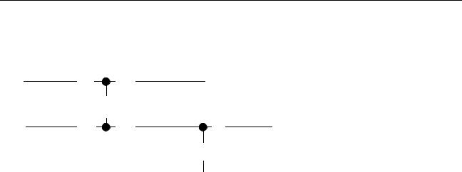
■The editor then verifies that all intersecting named nets B,C,C,B( and A,A,B,B) are taps of A,B,C.
A,B,C |
|
A,A,B,B |
1 |
2 |
|
|
3 |
|
C,B |
|
B,C |
4 |
5 |
6 |
|
|
7 |
Multiple-Bit Wire Naming Conventions
You can connect multiple-bit wires in your design using any one of the following naming conventions:
■Using Vector Expressions in Multiple-Bit Wire Names on page 105
■Using Vector Expressions in Multiple Signals on page 106
■Evaluating Vector Expressions in Multiple-Bit Wire Names on page 106
■Using Prefix Repeat Operators in Multiple-Bit Wire Names on page 106
■Using Suffix Repeat Operators in Multiple-Bit Wire Names on page 107
Using Vector Expressions in Multiple-Bit Wire Names
A multiple-bit wire name can be a bundle, a bus, or a combination of the two. You can improve readability in your designs by shortening multiple-bit wire names.
To indicate that multiple bits of one wire carry similar information, give each bit the same base name. Then add a suffix to each bit name to distinguish the signals.
For example, to show four bits of a wire with a common base name (DATA), but with individual suffixes <0>( , <1>, <2>, and <3>), assign the following names: DATA<0>, DATA<1>,
DATA<2>, and DATA<3>.
October 2002 |
105 |
Product Version 5.0 |

Virtuoso Schematic Composer User Guide
Understanding Connectivity and Naming Conventions
Using Vector Expressions in Multiple Signals
To name a wire that contains multiple signals with the same base name, specify the base name followed by a vector expression. The vector expression can be
■A list of the individual bit numbers separated by commas and enclosed with angle brackets.
For example, DATA<2,1,0> represents DATA<2>, DATA<1>, and DATA<0>.
■A range of numbers containing a lower and upper bound and, optionally, an increment value. The numbers are separated with colons and enclosed with angle brackets.
For example, DATA<1:7:2> represents
baseName <lowerBound : upperBound : [incrValue]>
Use a positive integer for incrValue. If you do not specify an increment value, the editor uses 1.
The ordering of the bits in a bus is important when you are connecting the bus to a pin that has a width greater than 1.
Evaluating Vector Expressions in Multiple-Bit Wire Names
The system evaluates vector expressions in multiple-bit wire names as follows:
■The vector expression DATA<0:3:2> names a 2-bit bus containing DATA<0> and
DATA<2>.
■The vector expression DATA<1:3:2> names a 2-bit bus containing DATA<1> and
DATA<3>.
■The vector expressions DATA<0:3> and DATA<0:3:1> are equivalent names that generate a 4-bit bus containing DATA<0>, DATA<1>, DATA<2>, and DATA<3>.
If the lower bound is larger than the upper bound, the editor generates the bit numbers in descending order, as follows:
■The vector expression DATA<2:0> generates a 3-bit bus that contains DATA<2>,
DATA<1>, and DATA<0>.
Using Prefix Repeat Operators in Multiple-Bit Wire Names
A multiple-bit wire name can be a bundle, a bus, or a combination of the two. You can improve readability in your designs by shortening multiple-bit wire names.
October 2002 |
106 |
Product Version 5.0 |