Virtuoso XL Layout Editor User Guide
Using the Virtuoso Custom Placer
(partition partition1
(shape rectangle ((5.300000 3.050000) (13.500000 10.600000))) (cell /P4)
(cell /P6) (cell /P7) (cell /P2)
(cell /P12)
)
Setting Placement Planning
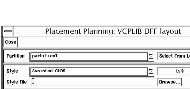
You define where in the layout you want to place transistors and other design elements with the Place – Placement Planning command and the Placement Planning form.
Note: Before you can set the placement planning, you or the library developer must first define thecomponent types for placement. Components that have types assigned to rows can only be placed in these rows.
There are two row definition modes for the Placement Planning form:Assisted and UserDefined.
■The assisted mode automates typical styles of MOS and standard cell placement
December 2002 |
287 |
Product Version 5.0 |
Virtuoso XL Layout Editor User Guide
Using the Virtuoso Custom Placer
■The user-defined mode offers greater flexibility but less automation and supports both transistorand cell-level placement
Assisted CMOS Placement
The Assisted CMOS row definition mode helps you define rows that fit your area budget. You can change the independent design variables that constrain the row shapes and observe their effect on area utilization and folded transistor widths.
Limitations
The component-assisted mode restricts the placement style to the most typical arrangements. There are a few limitations that are not present in the user-defined row definition mode:
■All rows must be horizontal or vertical
■All rows have the same width and span the entire placement region
Note: Row width can vary if the region is polygonal.
■Each row contains either NMOS or PMOS devices but not both and not any other component types
■The number of N and P rows is the same
■There is a regular arrangement of alternating N and P rows that follows one of these patterns:
NP
PN
December 2002 |
288 |
Product Version 5.0 |

Virtuoso XL Layout Editor User Guide
Using the Virtuoso Custom Placer
NPPN
PNNP
■All rows have the same device alignment relative to the devices in adjacent rows: inside, outside, or center
■Device rotation depends on the row and pattern.
■The rows can extend outside of the boundary/partition
Note: The placer can only place within the boundary/partition
If any of these limitations is not acceptable, you can either
■Define the rows in the user-defined mode
■Define the rows as completely as possible using the component-assisted mode and then refine the definitions in the user-defined mode
■Use assisted mode on either standard cell or MOS, but not both at the same time.
About Calculated Values
For both NMOS and PMOS transistors, the system calculates the number of transistors and the minimum, maximum, and average transistor widths. To update the displayed values, after altering variables, select Calculate Estimate.
The system also calculates the normalized percentage of Within Row and Between Row area utilization for the placement region. (In other words, a value of 100% in the Within Row field means that the entire width of the placement region is used by the devices). If there are too many devices to fit within the placement region, rows may overlap or extend outside the placement region. In this case, one or both of the Region Utilized values at the bottom of the form may be greater than 100%.
Using the Assisted CMOS Mode
To use the Assisted CMOS row definition mode,
1. Choose Place – Placement Planning.
December 2002 |
289 |
Product Version 5.0 |
Virtuoso XL Layout Editor User Guide
Using the Virtuoso Custom Placer
The Placement Planning form appears
2.Specify a partition name.
You can select a partition by clicking on Select From Layout and then clicking in the layout window to select the partition.
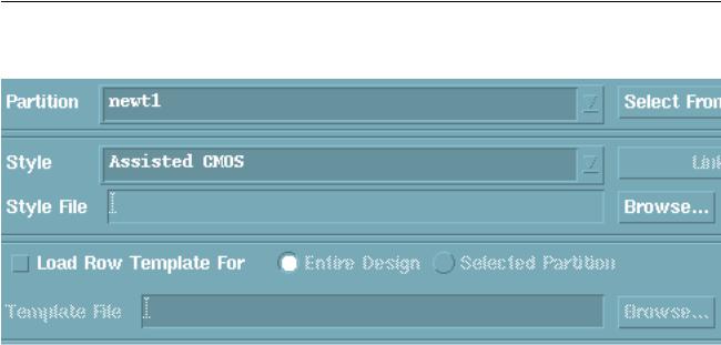
3.Change the Style to Assisted CMOS.
4.Click on Region to;
The placement region should be contained within the partition. For example, you might restrict assisted placement to the lower part of the partition, leaving the upper part available for manual placement. Or, you might leave space around the periphery for routing.
Type the dimensions of the drawing region in the Width and Height fields.
Type the X and Y coordinates of the location where you want the row in the Origin fields.
You can see the X and Y coordinates of the cursor position in the status line at the top of the layout window. If you do not type any coordinates, the new row is placed at the lower left corner of the design boundary.
Specify the placement region manually in the layout window, select Draw and the you are prompted to point at the first corner of the region’s rectangle.
December 2002 |
290 |
Product Version 5.0 |
Virtuoso XL Layout Editor User Guide
Using the Virtuoso Custom Placer
Important
When targeting a partition for assisted row generation, the estimator uses the entire partition area in its calculation.You can optionally specify a region within the partition by using the Draw option. If a region is defined the estimator will use the region area instead of the partition area.
Click Delete to remove the region created by the Draw option.
December 2002 |
291 |
Product Version 5.0 |
Virtuoso XL Layout Editor User Guide
Using the Virtuoso Custom Placer
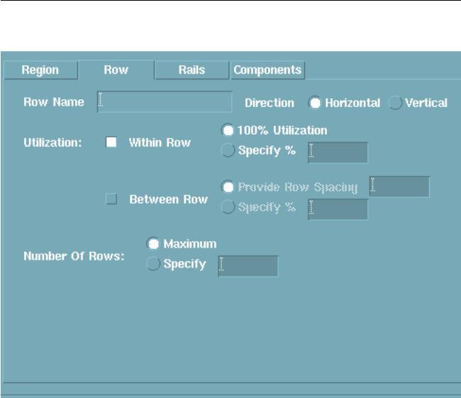
5. Select Row to update the row properties.
Note: If rows are already defined, change the Style to Manual User-Defined and the row information is displayed at the bottom of the Placement Planning form.Click on the row that you want to edit. The Row properties are updated in the Name field.
6. Set the orientation (Direction) of the row(s).
December 2002 |
292 |
Product Version 5.0 |
Virtuoso XL Layout Editor User Guide
Using the Virtuoso Custom Placer
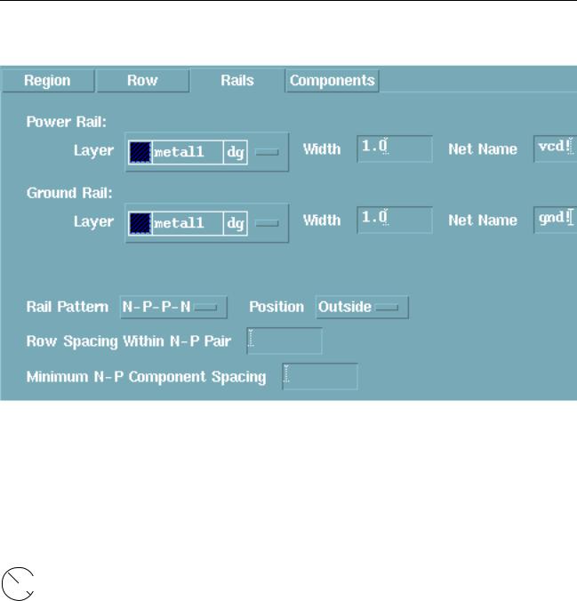
7. In the Rail section of the form;
Choose a layer and type values in the Net Name and Width fields for power and ground.
The layers are valid layers that are not used as vias or contacts.
In the Rail Pattern cyclic field, choose a pattern for the alternating N and P rows.
In the Position cyclic field determines the position of the rail relative to the row(Inside, Outside, or Center).
Caution |
Do not add a u at the end of a value for rail width and spacing rules because the value will be converted to 0.000001. For example, 12u will be converted to 0.012.
To create non-rectangular regions follow the steps below;
1.Select Place-Partitioning and create a partition for the components.
2.Select Place-Placement Planning and change the Style to Assisted CMOS.
December 2002 |
293 |
Product Version 5.0 |
Virtuoso XL Layout Editor User Guide
Using the Virtuoso Custom Placer
3.Select the partition by changing the Partition field to the partition name.
4.Select Draw and you are prompted to draw a region. Create the region inside of the partition.
5.Select Calculate Estimates. The rows are created and the row statistics are displayed at the bottom of the Placement Planning form.
6.Draw another separate region that doesn’t overlap the previous region (area now contains rows) using the Draw option.
7.Select Calculate Estimates. The rows are created and the row statistics are displayed at the bottom of the Placement Planning form.
Note: The final utilization must be calculated by hand using the row statistics from both regions.
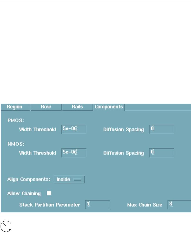
8.In the Component section of the form,
Caution |
Do not add a u at the end of a value for spacing rules because the value will be converted to 0.000001. For example, 12u will be converted to 0.012.
December 2002 |
294 |
Product Version 5.0 |
Virtuoso XL Layout Editor User Guide
Using the Virtuoso Custom Placer
In the Alignment cyclic field, chooseInside, Outside, or Center.
N-row
P-row
N-row
P-row
P-row |
|
|
|
|
|
|
|
|
|
|
|
|
|
|
|
|
|
|
P-row |
||||
|
|
|
|
|
|
|
|
|
|
|
|
|
|
|
|
|
|
||||||
|
|
|
|
|
|
|
|
|
|
|
|
|
|
|
|
|
|
||||||
|
|
|
|
|
|
|
|
|
|
|
|
|
|
|
|
|
|
|
|
|
|
|
|
|
|
|
|
|
|
|
|
P-row |
|
|
|
||||||||||||
|
|
|
|
|
|
|
|
|
|
|
|
|
|
|
|
|
|
|
|||||
|
|
|
|
|
|
|
|
|
|
|
|
|
|
|
|
|
|
|
|||||
|
|
|
|
|
|
|
|
|
|
|
|
|
|
|
|
|
|
||||||
|
|
|
|
|
|
|
|
N-row |
|
|
|
|
|
|
|
|
|
|
N-row |
||||
|
|
|
|
|
|
|
|
|
|
|
|
|
|
|
|
|
|
|
|
|
|
|
|
|
|
|
|
|
|
|
|
|
|
|
|
|
|
|
|
||||||||
N-row |
|
|
|
|
|
|
|
|
|
|
|
|
|
|
|
|
|
|
|
||||
|
|
|
|
|
|
|
|
|
|
|
|
|
|
|
|
|
|
|
|
|
|||
|
|
|
|
|
|
|
|
|
|
|
|
|
|
|
|
|
|
|
|
|
|
|
|
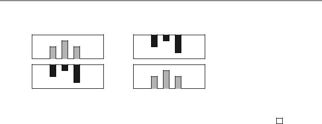
Inside (NPPN pattern) |
Outside (NP pattern) |
|
|
Center |
|||||||||||||||||||
Note: Alignment can be either top, bottom, or center for horizontal rows or right, left, or center for vertical rows.
Set the alignment of the component(s).
Type in the minimum width (Width Threshold) and required diffusion space between components within the row (Diffusion Spacing) for the PMOS and NMOS transistors.
9.To place only the devices for the selected component below the prBoundary select Regenerate All. The Update Layout option at the bottom of the Placement Planning form updates the current layout with the components and deletes existing components. This option is used on a selective basis based on the selected partition and style.
December 2002 |
295 |
Product Version 5.0 |
Virtuoso XL Layout Editor User Guide
Using the Virtuoso Custom Placer
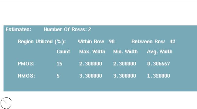
10.Click Calculate Estimate to calculate the row count, area utilization, device count, and device widths.
Caution |
The estimator will design the rows so as to avoid any preplaced components even if they are a part of the estimator computation. You should move these components out of the placement region before invoking the estimator. (needs to be put in for all types of styles)
The system regenerates folded transistors using the new values. The section at the bottom of the form is updated with the percentage of the region utilized and width information about the PMOS and NMOS components.
11.Evaluate the device counts against the need to generate equal numbers of P and N rows. Evaluate the area utilization based on routability considerations. If necessary, change the Number of Rows or PMOS Width Threshold or NMOS Width Threshold for folding. Click Calculate Estimate to update the calculated estimates.
If necessary, redefine the placement region and begin again with Step 4.
Note: After you click Calculate Estimate, if you make extensive changes to device folding and chaining choices (either through automatic layout generation or interactive device folding), the estimates you calculate in Step 10 may become invalid.
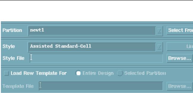
Using the Assisted Standard Cell Mode
To use the Assisted Standard Cell row definition mode,
1. Select Place – Placement Planning.
December 2002 |
296 |
Product Version 5.0 |
Virtuoso XL Layout Editor User Guide
Using the Virtuoso Custom Placer
The Placement Planning form appears
2.Change the Style to Assisted Standard-Cell.
3.In the Region section;
Type the dimensions of the row(s) in the Width and Height fields.
Type the X and Y coordinates of the location where you want the row in the Origin field.
You can see the X and Y coordinates of the cursor position in the status line at the top of the layout window. If you do not type in any coordinates, the new row is placed at the lower left corner of the design boundary.
To specify the placement region manually in the layout window, click Draw.
The layout window prompts you to point at the first corner of the region’s rectangle.
December 2002 |
297 |
Product Version 5.0 |
Virtuoso XL Layout Editor User Guide
Using the Virtuoso Custom Placer
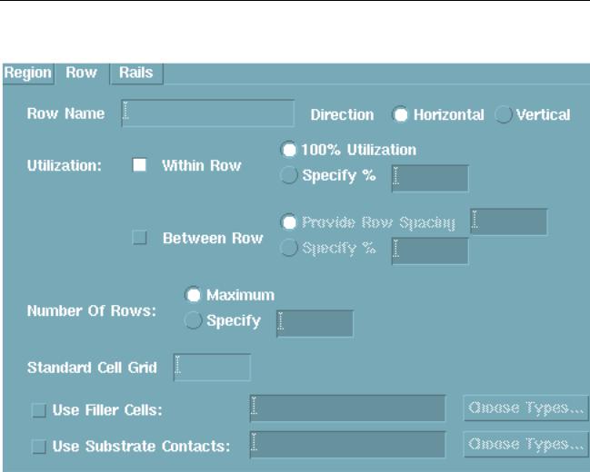
4. In the Row section of the form
Type the name of the row(s) to be designed in the Name field.
Set the orientation (Direction) of the row(s).
If you want to use filler cells that you have defined in the Edit Component Types form between the other cells in the row, click Use Filler Cells and type the names of the
filler cells into the field or clickChoose Types and choose the names of the filler cells from the list that appears in the Choose Component Types form. You must also specify a type when using the Substrate Contacts option. Use STDSUBCONT as the
Component Class.
December 2002 |
298 |
Product Version 5.0 |
Virtuoso XL Layout Editor User Guide
Using the Virtuoso Custom Placer
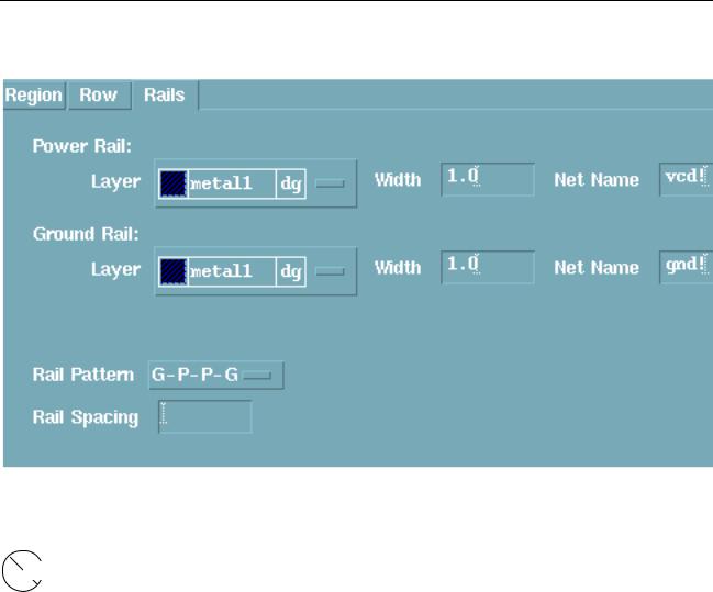
5. In the Rails section of the form
If applicable, choose a layer and type values in the Net Name and Width fields for power and ground nets.
Caution |
Do not add a u at the end of a value for rail spacing rules because the value will be converted to 0.000001. For example, 12u will be converted to 0.012.
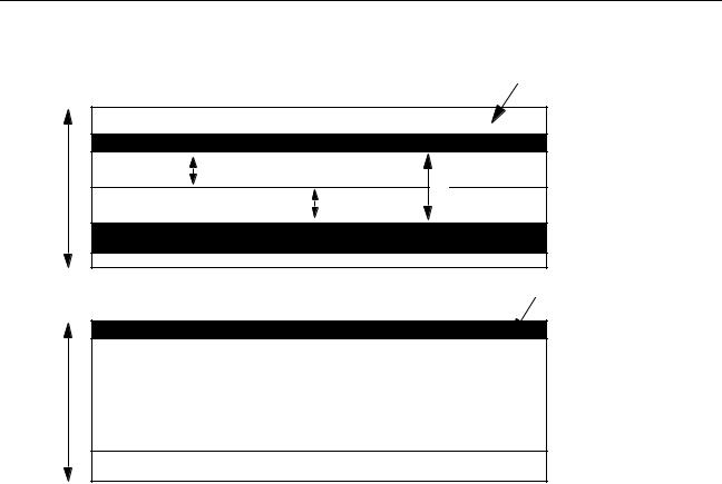
Rail Spacing.for Assisted Standard Cell mode
If no spacing value is supplied, the default behavior is to attach each rail within the row. The top of the power rail would be aligned to the top of the row, the bottom of the ground rail would be aligned to the bottom of the row.
If a spacing value is supplied, the spacing is applied between the two rails generated and centered within the row. For example; if you specify a spacing of 0 the rails will abut at the centerline (or middle) of the row. If a spacing of 2 is specified, there will be a separation of 2 between the upper and lower rail. Spacing of 1 above center and spacing of 1 below the centerline of the row.
December 2002 |
299 |
Product Version 5.0 |
Virtuoso XL Layout Editor User Guide
Using the Virtuoso Custom Placer
Spacing is provided
H |
S/2 |
|
S |
||
|
||
|
S/2 |
Spacing is not provided
H
|
|
|
|
December 2002 |
300 |
Product Version 5.0 |
|
Virtuoso XL Layout Editor User Guide
Using the Virtuoso Custom Placer
In the Pattern cyclic field, choose a pattern for the alternating ground and powerG( and P) rows.
Vdd
Gnd  PG
PG
Gnd
Vdd  GP
GP
PGGP rails not shared
GND
GP
Vdd
PG
Gnd
GPPG shared rails
6.In the Spacing field, type in the spacing you want between the rails.
7.Click Calculate Estimate to calculate the row count, area utilization, device count, and device widths.
The section at the bottom of the form is updated with the percentage of the region utilized.
If you choose to use the Regenerate All option all standard cells are regenerated once the Update Layout option is invoked. Or you can use the Generate Only Missing Components option and the missing components will be created. Generation/ regeneration only affects standard cells within the chosen partition.
Note: To modify the size of a rail, change the Rail information and then click Calculate
Estimate.
December 2002 |
301 |
Product Version 5.0 |
Virtuoso XL Layout Editor User Guide
Using the Virtuoso Custom Placer
8.Evaluate the device counts against the need to generate equal numbers of PG to GP rows. Evaluate the area utilization based on routability considerations. If necessary, change the Width or Height fields or the Width Threshold for folding. Click Calculate
Estimate to update the calculated estimates.
Note: After you click Calculate Estimate, if you make any changes to row definitions (either through automatic layout generation or interactive device folding), the estimates you calculate in Step 8 will become invalid.
9.Click Apply to save your row definitions.
Manual User-Defined Row-Based Placement
The Manual User-Defined mode for row definition lets you define row boundaries flexibly. For example, you can draw rectangles to delimit individual rows. Use the manual mode for placements above the device level or for MOS device placement styles that are not accommodated in the Assisted MOS mode.
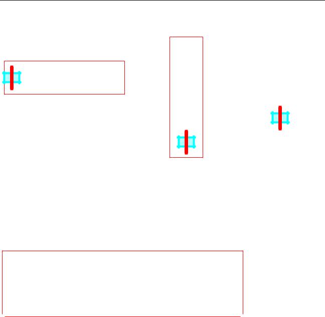
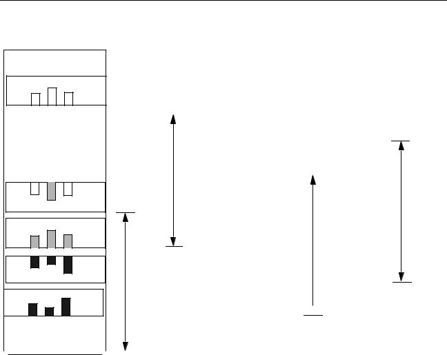
Figure 9-2 on page 302 shows an example of a placement region with four rows. Rows 1 and 2, the lower rows, span only half the placement region. Rows 3 and 4 span the entire placement region.
Figure 9-2 Examples of Rows
Defining Rows Manually
To define rows or columns manually,
1. Select Place – Placement Planning.
December 2002 |
302 |
Product Version 5.0 |

Virtuoso XL Layout Editor User Guide
Using the Virtuoso Custom Placer
The Placement Planning form appears.
2.Change the Style to Manual User-Defined.
3.Select General to define one or more rows.
Type the name of the row(s) to be designed in the Row Name field.
Set the orientation (Direction) of the row(s).
Type the dimensions of the row(s) in the Width and Height fields.
Click Draw and draw the shadow of the row. The row is not created until the Create button is invoked.
Type in the number of rows you want in the Number of Rows to Create field.
If Number of Rows to Create is greater than 1, then this will create an array of rows with the same devices and attributes at a fixed spacing between adjacent rows.
Type the X and Y coordinates of the location where you want the first row in the
Origin field.
You can see the X and Y coordinates of the cursor position in the status line at the top of the layout window. If you do not type in any coordinates, the new row is placed at the lower left corner of the design boundary.
In the Spacing Between Rows field, type the spacing you want between rows.
Caution |
Do not add a u at the end of a value for spacing rules because the value will be converted to 0.000001. For example, 12u will be converted to 0.012.
4.In the Types section on the form,
a.Select Edit and the Choose Component Types form appears
b.Select the component type and click OK. The selected component type appears in the Component Type(s) field.
c.Specify a Component Grid, Reference Point for Type and Row, Offset, and Orientations.
d.Select Create and the component type is displayed in the Types field box.
e.To change any of the component types properties select the component type in the
Types field and change the properties on the form. SelectUpdate and the component type properties are updated.
December 2002 |
303 |
Product Version 5.0 |

Virtuoso XL Layout Editor User Guide
Using the Virtuoso Custom Placer
5.In the Rails section of the form,
a.Specify the Layer, Width, and Net Name of the rail.
b.Change the Reference Point for the Row and Rail to be either Bottom, Top, or
Center.
c.Specify an Offset.
d.Click Add and the rail is displayed in the Rails field.
e.To change any of the rail properties, select the rail in the Rails field and change the properties on the form. Click Update to update the rail with the new properties.
Drawing Rows
You can define rows by drawing them, one at a time, in the layout window. SelectDraw and define the placement region for assisted MOS or cells.
Redefining a Row
Rows are actual database objects you can move and stretch graphically. To graphically edit rows make sure that the Row drawing layer purpose pair is a valid layer and made selectable in the Layer Selection Window (LSW).
You can delete a row either by changing the Style to Manual User-Defined mode. The rows are displayed at the bottom of the Placement Planning form. You can select a row and use the Delete Selected option to delete the selected tows, or graphically selecting the row in the layout window and then deleting it.
Setting Up Power and Ground Rails
You can define arrays of multiple rows in one step to create alternating rows with the same definitions. This arrangement facilitates the layout of power lines.Figure 9-3 on page 305 shows a portion of a buffer array with alternating NMOS and PMOS transistors in columns.
December 2002 |
304 |
Product Version 5.0 |
Virtuoso XL Layout Editor User Guide
Using the Virtuoso Custom Placer
Figure 9-3 Alternating Vertical NMOS and PMOS Rows
N-row
|
|
|
|
|
|
|
|
|
|
|
|
|
|
|
|
|
|
|
|
|
|
|
|
|
|
|
|
|
|
|
|
|
|
|
|
|
|
|
|
|
|
|
|
|
|
|
|
|
|
|
|
|
|
|
|
|
|
|
|
|
|
|
|
|
P-row |
|
|
|
|
NPPN Array Spacing |
|||||||
|
|
|
|
|||||||||
|
|
|
|
|
|
|
|
|
|
|||
|
|
|
|
|
|
|
|
|
|
|||
P-row |
|
|
|
|||||||||
|
|
|
|
|
|
|
|
|||||
|
|
|
|
|
|
|
|
|||||
|
|
|
|
|
|
|
|
|
|
|
|
|
|
|
|
|
|
|
|
|
|
|
|
|
|
|
|
|
|
|
|
|
|
|
|
|
|
|
|
|
|
|
|
|
|
|
|
|
|
|
|
|
|
|
|
|
|
|
|
|
|
|
|
|
|
|
|
|
|
|
|
|
|
|
|
|
|
N-row
N-row
NPPN Array Spacing
P-row
P-row
 NPPN Array Spacing
|
|
|
|
|
|
|
|
|
|
|
|
NPPN Array Spacing |
N-row |
|
|
|
|
|
|
|
|
||||
|
|
|
|
|
|
|||||||
To define the placement style for these eight rows, you define two arrays of components. To define the PMOS rows, follow these steps:
1.Choose Place – Placement Planning.
2.Choose Manual User -Defined.
3.Create the N row as the bottom row.
4.Create the P row above the N row.
5.Create another P row.
6.Create the N row which is on the top.
7.Set Num Of Rows to Create to 2.
The row setup is now complete.
December 2002 |
305 |
Product Version 5.0 |
Virtuoso XL Layout Editor User Guide
Using the Virtuoso Custom Placer
For other arrangements of power lines between rows, you might, for example, need to define arrays of every fourth or eighth row in order to achieve the desired mirroring pattern.
About Horizontal and Vertical Rows
You can define both horizontal and vertical rows for placement. To do this, set the desired direction as you define each row or set of rows.
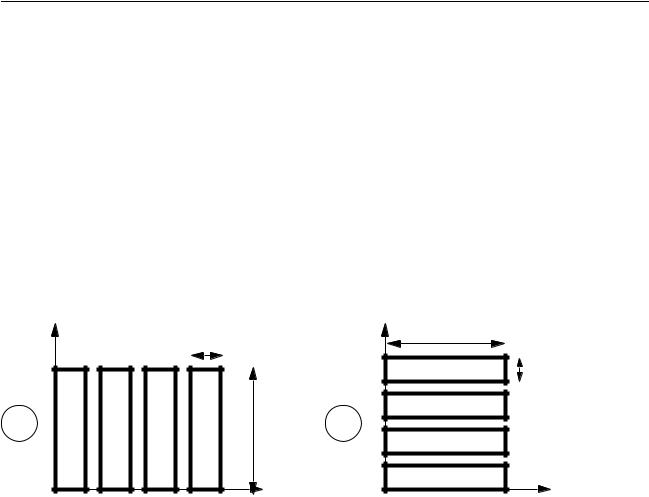
Figure 9-4 on page 306 shows how the Width and Height parameters should be set for horizontal and vertical rows. As this figure illustrates, theWidth is measured along the direction of the rows.
Figure 9-4 Setting Width and Height for Horizontal and Vertical Rows
1
(0,0)
height |
width |
|
|
|
height |
width |
2 |
|
|
|
(0,0) |
1.Row direction is Vertical, Width is 10, Height is 4, Spacing is 2.
2.Row direction is Horizontal, Width is 10, Height is 4, Spacing is 2.
About Device Orientation
There is no implied rotation of devices in vertical rows. The Orientation value you specify in the Placement Planning form is always relative to the master cell coordinates. Figure 9-5 on page 307 shows the undesired result of placing the same device with orientation R0 (unrotated) in both a horizontal and vertical row.
December 2002 |
306 |
Product Version 5.0 |