


Virtuoso XL Layout Editor User Guide
Editing Your Layout with Virtuoso XL Layout Editor
Information About Online Forms
■Assign Nets Form on page 247
■Edit Component Types Form on page 247
■Move Form on page 249
■Set Transistor Folding Form on page 249
■Show Incomplete Nets Form on page 250
■Stretch Form on page 252
■Virtuoso XL Alignment Form on page 253
Assign Nets Form
Create enters in the list of net names the new net name you type in the entry field.
Delete deletes from the list of net names the name you type in the entry field or select in the list of net names if no objects are attached to that net.
The entry field above the list of net names has a search mechanism that highlights in the list box the net name you type in the field.
Edit Component Types Form
The Edit Component Types form lets you create and modify placement component types for libraries or cells.
Scope radio buttons let you set the scope of the component types you are defining.
Components that you place in the cells encompassed by the scope share the component type definitions you create in the lower part of the form.
Lib assigns these type definitions to the library containing the current cellview.
Current assigns these type definitions to the current cellview only.
Ref Libs assigns these type definitions to the specified reference library from the cyclic field.
Type is the name of a component type. Enter new type names in this field, or click on type names in the cyclic field to select them for editing.
December 2002 |
247 |
Product Version 5.0 |

Virtuoso XL Layout Editor User Guide
Editing Your Layout with Virtuoso XL Layout Editor
Add creates a new type with the name shown in the Type Name field.
Delete immediately removes the type in the Type Name field from the types defined for the current scope. If you delete a type accidentally, you can select Cancel to discard all of your changes in the Edit Component Types form.
Add Selected Components adds the instances currently selected in the layout window to the Components in Type list. Use this button to select which instances should be in which types.
Important
You cannot use this command to define chaining and folding parameters for instances. All instances of a master must share the same parameter values, and you must define those values on the master cell (by including the master in the
Components in Type list).
Cells in Design lists all of the cells in the library. You can highlight the cells by click on them, or typing a quoted library and cell name in the type-in field. The syntax is:
"MYLib Mycell"
Components in Type lists the masters and instances belonging to the current Type.
>>> moves the selected components to the Components in Type list.
Delete Component deletes components that you have highlighted in the Components in Type list field.
Edit parameters is a cyclic field containing the names of the required and optional placement parameters. the name of a parameter shared by the cells in a type. Enter new names in this field, or click on parameter names in the list box to select them for editing. For information about each parameter, see “MOSransistorT Stacking and Folding Parameters” on page 228
Component Class lets you identify MOS transistors suitable for chaining, folding, and the
Assisted MOS placement style. For MOS transistors, set this field toNMOS or PMOS as appropriate or set STDCELL, STDSUBCONT or FILLER for those design components. For all other devices, set this field toUndefined.
You can have multiple devices assigned to the NMOS and PMOS component types. This would typically be the case for multiple voltage designs.
December 2002 |
248 |
Product Version 5.0 |
Virtuoso XL Layout Editor User Guide
Editing Your Layout with Virtuoso XL Layout Editor
Move Form
Snap Mode controls the direction in which you can move the object.
anyAngle |
diagonal |
orthogonal |
horizontal |
vertical |
(default) |
|
|
|
|
Change To Layer, when on, lets you move a shape to another layer. Choose the new layer from the cyclic field, which displays all the available valid layers.
Delta X/Y allows you to specify the distance to move the selected objects in the X and/or Y direction.
Apply XY invokes the distance specified in theDelta X/Y fields.
Display Draglines, when on, displays rubberbanding lines that connect pins of the object you are moving to pins of the nearest objects.
Constraint Assisted Control allows objects to be moved only in ways that satisfy the constraints entered using the constraint manager.
together moves preselected objects in the layout as a group. individually moves preselected objects in the layout individually.
ignore specifies that constraints have no effect on objects in the layout when they are moved.
Rotate rotates the component 90 degrees counterclockwise.
Sideways mirrors the component on the Y axis (flips it horizontally).
Upside Down mirrors the component on the X axis (flips it vertically).
Set Transistor Folding Form
Transistor Name displays the name of the first transistor you selected.
December 2002 |
249 |
Product Version 5.0 |

Virtuoso XL Layout Editor User Guide
Editing Your Layout with Virtuoso XL Layout Editor
Transistor width as specified in the schematic displays the value of the width property of the transistor in the schematic.
Number of Fingers lets you enter the number of fingers (divisions) into which you want to fold the transistor. Entering a value in the Number of Fingers field causes the appearance of the Set Finger Widths option button.
Set Finger Widths, when turned on, changes the Set Transistor Folding form to include new fields that let you enter the width of each finger.
Chain Fingers, when active, allows the software to abut the fingers into stacks.
Total Width displays the total value of the all widths you enter in the Width fields.
Add Finger adds another Width field to the form to let you enter the width of an additional finger.
Same Width sets all the values in the Width fields to the same width (totaling the same value as specified in the schematic, unless you override that value in the entries you make in the Width fields).
Width lets you enter a separate width for each finger.
Delete removes the Width field and decreases the number in theNumber of Fingers field by 1.
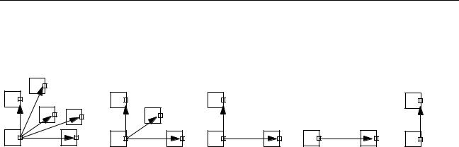
Show Incomplete Nets Form
Cellview displays the library, cell, and view name of the layout window on which the Show Incomplete Nets form is focused.
Class displays class names in the list boxes and prepares the search fields for class names.
Classes are created in the Constraint Manager form.
Net displays net names in the list boxes and prepares the search fields for net names.
Color choice cyclic field:
Cycle lets the software assign the next y0–y9 entry layer in the color choice cyclic field to the next flight line you choose.
The y1–y9 entry layers let you assign one single color for all the flight lines. You cannot assign the y0 layer as a single color for all flight lines because it is the default layer.
December 2002 |
250 |
Product Version 5.0 |
Virtuoso XL Layout Editor User Guide
Editing Your Layout with Virtuoso XL Layout Editor
As Is keeps the colors currently assigned from the y1–y9 entry layers in the color choice cyclic field.
Set Color sets the color of all incomplete nets highlighted in the Incomplete list box and highlighted in the layout window to the drawing layer color shown in the color choice cyclic
field.
Search lets you type one or more net or class names (separated by a space) to be highlighted in the Incomplete or Complete list boxes and in the layout window. You cannot use the wildcard character (*) in this field, but typing the initial characters of net names highlights all names in both lists beginning with the specified character(s).
Incomplete
The type-in field lets you type partial or complete names of nets to be highlighted in the Incomplete list box and displayed in the layout window (as long as they are incomplete) when you click Apply.
The list box lets you select the names of nets you want to display or to which you want to assign a color. You can use Control click to select more than one or to deselect selected net names.
Select All displays flight lines for all incomplete nets in the design when you clickApply.
Select from Display lets you click on pins and instances in the layout window to select them and displays them when you click Apply.
Less truncates the form so that it does not display the Complete nets list box or the Zoom features; the button label changes to More.
More expands the truncated version of the form to include the Complete nets list box and the Zoom features; the button label changes to Less.
Complete
The type-in field lets you type in partial or complete names of nets to be highlighted in the
Complete list box and displayed in the layout window (only if they become incomplete) when you click Apply. This capability lets you mark nets of critical importance so that they show up if their connectivity is lost.
The list box lets you select the names of nets you want to display or to which you want to assign a color. You can use Control click to select more than one or to deselect selected net names.
Clear All Selections removes the display of flight lines for all incomplete nets in the design when you click Apply.
December 2002 |
251 |
Product Version 5.0 |