

Camenzind_Analog design chips
.pdfCamenzind: Designing Analog Chips |
Chapter 1: Devices |
Fig. 1-4: The first step: A light-sensistive and etch-resistant layer (photoresist) is spread on the wafer and exposed to light through the mask.
Fig. 1-5: The photoresist is developed like a photograph and the wafer is ready for etching.
Fig. 1-6: The oxide is etched away and the photoresist is removed.
Fig. 1-7: A gas containing N-type dopants (boron. arsenic or antimony) diffuses slowly into the surface of the wafer at high temperature.
the frequency of the light, the greater the detail, so ultra-violet light or even x-rays are used.
The photoresist is then developed and the portions not exposed to light are washed off. (There are both positive and negative photoresists; you have the choice of removing the areas
which are either exposed or not exposed to light).
Next the entire wafer is immersed in an acid which removes the oxide in the areas where it is not protected by the photoresist. In more modern processes a plasma is used; acid etches not only downward but also slightly sideways underneath the photoresist, while plasma etches downward only.
The wafer is then placed into a furnace (a quartz tube heated to greater than 1000oC). A gas carrying the desired dopant (in this case boron, arsenic or antimony) swirls around the wafer and slowly diffused into the surface.
Note two important facts here: 1. There is a crowding of dopants near the surface of the silicon. With time they will diffuse deeper into the silicon, but there will always be more dopants near the surface. Thus any diffused region has a marked gradient. 2. Dopants not only diffuse downward, but also sideways. (Since supply is more limited at the very edge, the
Preliminary Edition September 2004 |
1-15 |
All rights reserved |
Camenzind: Designing Analog Chips |
Chapter 1: Devices |
side-ways diffusion extends to only about half the distance of the downward one). This places the junction (where n = p) underneath the oxide and is thus never exposed to the (dirty) environment.
After diffusion the exposed silicon surface is covered again by an oxide layer so that the wafer is ready for the next masking step, which could
be another diffusion or the etching of contact holes.
There is an important feature here, which should not go unnoticed. SiO2 is glass, which is transparent to light. The light is reflected at the bottom of the oxide by the
silicon and interference patterns are created, i.e. the sum of direct and the reflected light eliminates some frequencies. Thus the color of the oxide layer depends on its thickness. This not only makes for beautiful photographs but, more importantly, it allows subsequent masks to be precisely aligned with previous ones.
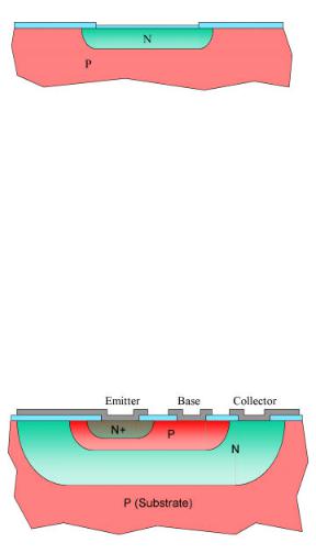
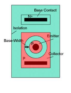
Here then is one form of an NPN transistor made with the planar process. The substrate (the starting wafer) is doped p-type as the silicon is grown. There are three diffusions in succession, the first being rather deep. After the diffusions, contact holes are made (with the same basic photoresist process), aluminum is deposited over the entire wafer, patterned (another photoresist step) and etched away where it is not wanted.
Alas, this transistor has a rather significant shortcoming: high collector resistance. The current has to flow through the region between the base and the substrate. That is the far end of the collector diffusion, the end which has the fewest dopant atoms and therefore the highest resistance.
Since the invention of the planar process a few more ways of fabricating have been added:
Epitaxy. If you strip a silicon wafer of its oxide and put it into a furnace which is filled with gas containing not only a dopant but also silicon, you can grow a doped single-crystal layer. As the atoms carried by the gas deposit themselves on the surface of the wafer, they will align
Preliminary Edition September 2004 |
1-16 |
All rights reserved |
Camenzind: Designing Analog Chips |
Chapter 1: Devices |
themselves according to the existing crystal structure.
You can also precede this by diffusing regions into the original wafer, so that you will have areas of high concentration underneath the epitaxial layer. Even though these regions are buried, it is still possible to align subsequent diffusions to them. When a diffused area is re-oxidized, a small amount of silicon is consumed (the Si in SiO2), thus creating a small depression in the surface. The edges of these depressions are visible at the top surface of the epitaxial layer, though the image tends to be blurry and is shifted (in most processes) along the crystal axis (around 45o).
Ion Implantation. You can literally shoot dopant atoms into silicon by electrically charging (ionizing) them and then accelerating them with a high voltage (several hundred thousand volts). The treatment is somewhat brutal, the newly arrived atoms don't end up neatly aligned in the crystal structure and an annealing heat cycle is necessary to let the atoms align themselves into a crystal structure.
The number of dopant atoms introduced is generally more accurate in ion implantation than in diffusion. Also you can aim implantation for a certain depth (but not very deep). In the subsequent heat cycle (and during subsequent diffusions) the dopant atoms will diffuse and thus widen the layer. The maximum concentration, however, is then not at the surface, but at a chosen depth.
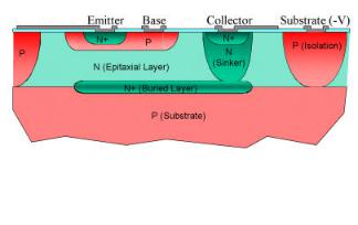
We now have arrived at a modern NPN transistor as made in a bipolar (or BICMOS) process. Before growing the epitaxial layer, a heavily doped (thus N+) buried layer is diffused (or ion implanted) into the p-type substrate. During epitaxy it diffuses somewhat, both into the substrate and the new epitaxial layer.
The next diffusion is the isolation. It is deep (and, therefore, also wide); it has to connect up with the substrate, so that the entire n-type collector region is surrounded by p-type regions. A second n- type diffusion connects up with the buried layer
(and the emitter N+ diffusion is used on top of it simply because it's available at no cost). Now the collector current has a (fairly) low-resistance path.
Preliminary Edition September 2004 |
1-17 |
All rights reserved |

Camenzind: Designing Analog Chips |
Chapter 1: Devices |
This transistor is isolated from its neighbors (and other components) as long as the substrate is held at the most negative voltage in the circuit (junction isolation). In this way the collector-substrate junction is always reverse-biased and only leakage current (pico-amperes) flows.
There are some flaws and limitations in the performance of this or any other bipolar transistor:
Early Effect, named after Jim Early, then at Fairchild, who was the first to explain it. Ideally the collector current should be equal to the base current multiplied by a constant gain (hFE or beta). But, as we have seen above, each p-n junction has two depletion layers. For the collector-base junction, one depletion layer extends into the collector, the other into the base. The base is almost always more heavily doped than the collector, so its depletion layer is fairly
shallow. However, the base |
|
240 |
|
|
|
|
|
|
|
|
|
|
|
|
|
|
|
|
|
|
|
|
|
|
|
|
|
|
|
|
|
|
|
|
|
|
|
|
|
|
|
|
|
|
|
|
|
is also very thin, so even a |
|
220 |
|
|
|
|
|
|
|
|
|
|
|
|
|
|
|
|
|
|
|
|
|
|
200 |
|
|
|
|
|
|
|
|
|
|
|
|
|
|
|
|
|
|
|
|
|
|
shallow depletion layer takes |
|
180 |
|
|
|
|
|
|
|
|
|
|
|
|
|
|
|
|
|
|
|
|
|
|
|
|
|
|
|
|
|
|
|
|
|
|
|
|
|
|
|
|
|
|
|
||
|
|
|
|
|
|
|
|
|
|
|
Early |
Effect |
|
|
|
|
|
|
|||||
up a significant portion of the |
|
160 |
|
|
|
|
|
|
|
|
|
|
|
|
|
|
|
|
|||||
|
|
|
|
|
|
|
|
|
|
|
|
|
|
|
|
|
|
|
|
|
|
||
|
140 |
|
|
|
|
|
|
|
|
|
|
|
|
|
|
|
|
|
|
|
|
|
|
base depth. As the collector |
/ µA |
|
|
|
|
|
|
|
|
|
|
|
|
|
|
|
|
|
|
|
|
|
|
120 |
|
|
|
|
|
|
|
|
|
|
|
|
|
|
|
|
|
|
|
|
|
||
|
|
|
|
|
|
|
|
|
|
|
|
|
|
|
|
|
|
|
|
|
|||
voltage increases, the |
Ic |
|
|
|
|
|
|
|
|
|
|
|
|
|
|
|
|
|
|
|
|
|
|
|
100 |
|
|
|
|
|
|
|
|
|
|
|
|
|
|
|
|
|
|
|
|
|
|
|
|
|
|
|
|
|
|
|
|
|
|
|
|
|
|
|
|
|
|
|
|
||
|
|
|
|
|
|
|
|
|
|
|
|
|
|
|
|
|
|
|
|
|
|
|
|
depletion layers widen. In |
|
80 |
|
|
|
|
|
|
|
|
|
|
|
|
|
|
|
|
|
|
|
|
|
|
|
|
|
|
|
|
|
|
|
|
|
|
|
|
|
|
|
|
|
|
|
||
|
60 |
|
|
|
|
|
|
|
|
|
|
|
|
|
|
|
|
|
|
|
|
|
|
the collector region this has |
|
|
|
|
|
|
|
|
|
|
|
|
|
|
|
|
|
|
|
|
|
|
|
|
40 |
|
|
|
|
|
|
|
|
|
|
|
|
|
|
|
|
|
|
|
|
|
|
|
|
|
|
|
|
|
|
|
|
|
|
|
|
|
|
|
|
|
|
|
|
||
little effect (as long as it |
|
20 |
|
|
|
|
|
|
|
|
|
|
|
|
|
|
|
|
|
|
|
|
|
|
|
|
|
|
|
|
|
|
|
|
|
|
|
|
|
|
|
|
|
|
|
||
|
0 |
|
|
|
|
|
|
|
|
|
|
|
|
|
|
|
|
|
|
|
|
|
|
doesn't hit the other side of |
|
0 |
|
1 |
|
|
2 |
3 |
|
|
|
4 |
|
|
|
|
|||||||
|
|
|
|
|
|
|
|
|
|
|
|
|
|
|
|
|
|
|
|
|
|
|
|
the collector), but in the base |
|
|
Vc/V |
|
|
|
|
|
|
|
|
|
|
|
|
|
|
|
|
1V/div |
|||
|
|
|
|
|
|
|
|
|
|
|
|
|
|
|
|
|
|
|
|
|
|
|
|
region it narrows the basewidth. Since the gain of a bipolar transistor is very much dependent on the base-width, the
gain simply increases as the effective base-width decreases.
If you draw a straight line, extending the slope (from 0.4 to 5 Volts) into the negative quadrant and let it intersect with the zero-current line, you get the Early Voltage. In this case, for a 5-Volt process, the Early voltage is 15 Volts. Depending on the chosen base-width, it can be less than that and the slope correspondingly steeper.
Gain versus Current. For any bipolar transistor the current gain falls off both at low and high current.
First, the low end. There is always a leakage current across any junction; for a perfectly clean surface this is the diffusion current. In the base-emitter junction this leakage current takes away a portion of the supplied base current. In our graph here the current shunted by leakage at
Preliminary Edition September 2004 |
1-18 |
All rights reserved |
Camenzind: Designing Analog Chips |
Chapter 1: Devices |
the low end (10nA Ie, or about 50pA Ib) amounts to 33% of Ib, i.e. the gain has dropped by one third.
If you extend this plot to much lower current, you will see the gain rise to almost infinity. This is nothing more than effect of the collector-base leakage current.
At the high end two effects take place simultaneously: 1. The number of electrons present in the base simply becomes so large that they are no longer the minority carriers and the whole effect comes to a halt. 2. The base current must flow
from the contact to the flat |
|
350 |
|
|
|
|
|
|
|
|
|
|
|
|
|
|
|
|
|
|
|
|
|
|
|
|
|
|
|
|
|
|
|
|
|
|
|
|
|
|
|
|
|
|
|
|
|
area between the emitter and |
|
300 |
|
|
|
|
|
|
|
|
|
|
|
|
|
|
|
|
|
|
|
|
|
|
|
|
|
|
|
|
|
|
|
|
|
|
|
|
|
|
|
|
|
|
|
||
collector. At low current this |
|
250 |
|
|
|
|
|
|
|
|
|
|
|
|
|
|
|
|
|
|
|
|
|
|
|
|
|
|
|
|
|
|
|
|
|
|
|
|
|
|
|
|
|
|
|
||
is no problem, the resistance |
|
|
|
|
|
|
|
|
|
|
|
|
|
|
|
|
|
|
|
|
|
|
|
|
|
|
|
|
|
|
|
|
|
|
|
|
|
|
|
|
|
|
|
|
|
||
|
|
|
|
|
|
|
|
|
|
|
|
|
|
|
|
|
|
|
|
|
|
|
|
|
|
|
|
|
|
|
|
|
|
|
|
|
|
|
|
|
|
|
|
|
|
|
|
in the base is sufficiently |
/ |
|
|
|
|
|
|
|
|
|
|
|
|
|
|
|
|
|
|
|
|
|
|
Gain |
200 |
|
|
|
|
|
|
|
|
|
|
|
|
|
|
|
|
|
|
|
|
|
|
|
|
|
|
|
|
|
|
|
|
|
|
|
|
|
|
|
|
|
|
|
|||
|
|
|
|
|
|
|
|
|
|
|
|
|
|
|
|
|
|
|
|
|
|
||
small. But as the collector |
Current |
150 |
|
|
|
|
|
|
|
|
|
|
|
|
|
|
|
|
|
|
|
|
|
current increases (and with it |
|
|
|
|
|
|
|
|
|
|
|
|
|
|
|
|
|
|
|
|
|
||
|
|
|
|
|
|
|
|
|
|
|
|
|
|
|
|
|
|
|
|
|
|
||
|
|
|
|
|
|
|
|
|
|
|
|
|
|
|
|
|
|
|
|
|
|
|
|
|
|
|
|
|
|
|
|
|
|
|
|
|
|
|
|
|
|
|
|
|
|
|
|
the base current), the |
|
100 |
|
|
|
|
|
|
|
|
|
|
|
|
|
|
|
|
|
|
|
|
|
|
|
|
|
|
|
|
|
|
|
|
|
|
|
|
|
|
|
|
|
|
|
||
|
|
|
|
|
|
|
|
|
|
|
|
|
|
|
|
|
|
|
|
|
|
|
|
resistance in this flat region |
|
50 |
|
|
|
|
|
|
|
|
|
|
|
|
|
|
|
|
|
|
|
|
|
|
|
|
|
|
|
|
|
|
|
|
|
|
|
|
|
|
|
|
|
|
|
||
of the base causes a |
|
|
|
|
|
|
|
|
|
|
|
|
|
|
|
|
|
|
|
|
|
|
|
|
|
|
|
|
|
|
|
|
|
|
|
|
|
|
|
|
|
|
|
|
|
|
|
significant voltage drop, and |
|
|
|
|
|
|
|
|
|
|
|
|
|
|
|
|
|
|
|
|
|
|
|
|
10n |
100n |
1µ |
10µ |
100µ |
|
|
|
1m |
10m |
|||||||||||||
|
|
|
|
|
|
|
|
|
|
|
|
|
|
|
|
|
|
|
|
|
|
|
|
the far end gets less current. Eventually, as the current is increased even more, only the edge of the emitter on the side of the base contact is active. Thus
the high-current capability of a bipolar transistor is determined not by the emitter area, but by the active emitter length, i.e. emitter periphery to which the base can supply current through low resistance. A good starting point for the maximum current (at which the gain drops to 50%) is 1.5mA per um of active emitter length, but this value varies from process to process.
To increase the current capability of a bipolar transistor you can
Preliminary Edition September 2004 |
1-19 |
All rights reserved |

Camenzind: Designing Analog Chips |
Chapter 1: Devices |
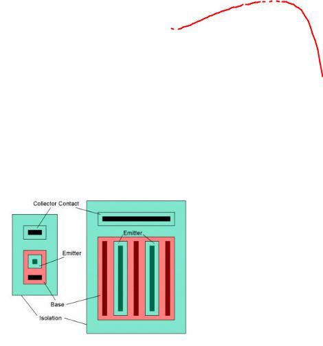
place base contacts on both sides of the emitter and lengthen the emitter. Shown here on the left is the top view of a minimum-geometry transistor and on the right a version for higher current.
To make the life of a designer easier, the isolation pattern is usually drawn as a rectangle and then inverted when making the mask, i.e. the isolation diffusion is actually between devices, not in the device area.
Many processes require that all contacts be the same size, in which case the contact rectangles must be broken up into small, identical (and properly spaced) squares.
Be aware, that transistors of different sizes (as drawn here) do not match well. At low current a large emitter area produces a higher gain than a small one, because the minority carriers have a higher chance to be captured by the collector. If you want to produce a precise ratio, use only one emitter size and identical base contacts. The emitters can be in a common base area and the collector size is of no consequence except for collector resistance (or saturation voltage).
Substrate Current. There is only leakage current across the collector-substrate junction, unless the transistor saturates.
Assume the collector is connected through a resistor to the positive supply voltage and the base is driven so hard that the collector voltage drops to near the potential of the emitter (termed
saturation). |
|
|
|
|
|
Collector |
||||||||||
|
|
|
|
|
|
|
|
|
|
|
|
|
|
|
|
|
There are now two diodes in parallel and |
|
|
|
|
|
|
|
|
|
|
|
|
|
|
|
|
|
|
|
|
|
|
|
|
|
|
|
|
|
|
|
|
|
the base current has two paths; the new one forms a |
|
|
|
|
NPN |
|
|
|
||||||||
|
|
|
|
|
|
|
|
|||||||||
PNP transistor with the NPN base becoming the |
Base |
|
|
|||||||||||||
|
|
|
|
|
|
|
|
|
|
|
|
|
|
|
|
|
emitter, the NPN collector the base and the |
|
|
|
|
|
|
|
|
|
|
|
|
|
|
|
|
|
|
|
|
|
|
|
|
|
|
|
|
|
|
|
|
|
|
|
|
|
|
|
|
|
|
|
|
|
|
|
|
|
|
substrate the collector. Since the NPN collector is |
|
|
|
|
|
|
|
|
|
|
|
|
|
PNP |
||
|
|
|
|
|
|
|
|
|
|
|
|
|
||||
|
|
|
|
|
|
|
|
|
|
|
|
|
|
|
|
|
much larger than its emitter, some (or all) of the |
|
|
|
|
|
|
|
|
|
|
|
|
|
|
|
|
|
|
|
|
|
|
|
|
|
|
|
|
|
|
|
|
|
base current flows to the substrate. |
|
|
|
|
|
|
|
|
|
|
|
|
|
|
|
|
|
|
|
|
|
|
|
|
|
|
|
|
|
|
|
|
|
There is little danger in this, except when |
|
|
|
|
|
Emitter Substrate |
||||||||||
|
|
|
|
|
|
|
|
|
|
|
|
|
|
|
|
|
you drive the base very hard, trying to get the |
|
Fig. 1-14: When an NPN |
||||||||||||||
lowest possible collector voltage, or if you have |
|
|
transistor saturates a |
|||||||||||||
many saturating NPN transistors. The path in the |
|
stray PNP device leaks |
||||||||||||||
substrate from a transistor to the -V connection has |
|
current to the substrate. |
||||||||||||||
|
|
|
|
|
|
|
|
|
|
|
|
|
|
|
|
|
some resistance. If the substrate current is so large |
|
|
|
|
|
|
|
|
|
|
|
|
|
|
|
|
that the voltage drop across this resistance can forward-bias some substratecollector junction on the way, you may get some really bad effects, including latch-up.
Maximum Voltage. To get a high operating voltage requires high resistivity - low doping concentration. But there is a price to be paid: the depletion regions become wide.
Preliminary Edition September 2004 |
1-20 |
All rights reserved |
Camenzind: Designing Analog Chips |
Chapter 1: Devices |
Let's use the integrated NPN transistor as an example. There are two depletion regions, one extending into the epitaxial layer from the base (downward and side-ways), the other into the epitaxial layer from the isolation. To make sure the first one does not reach the substrate (and thus
cause premature breakdown or punchthrough), the epitaxial layer must be deep - which means that the isolation diffusion must be deep, and thus wide.
Look at the left side of the transistor. The spacing between the
isolation (as drawn) and the base must accommodate the following: the side-ways diffusion of the isolation,
the isolation-collector depletion region,
a safety margin for possible misalignment, the collector-base depletion region and the side-ways diffusion of the base.
In addition there is also a high-voltage depletion layer each between the base and the sinker and the sinker and the isolation, as well as a deeper (and thus wider) sinker. All this adds up to a painfully large area.
The increase in area can be curbed somewhat by two measures: 1. Use an additional diffusion for the isolation by creating a P+ region directly underneath the normal one before growing the epitaxial. The two halves will then diffuse toward each other (up-down diffusion) and meet in the middle, thus requiring only half the depth and width; 2. Add more processing steps, creating both low-voltage and high-voltage devices on the same wafer.
The Miller Capacitance. As we have seen above, the bipolar transistor is a very non-linear (exponential) voltage amplifier and cannot thus normally be used as one. But is has a voltage gain, and a high one at that (several hundred is not uncommon).
There is an unavoidable junction capacitance between the collector and the base. If you feed a current with an ac signal into the base, the voltage change on the collector will be much larger than that on the base. Thus, looking into the base, the junction capacitance appears multiplied by the voltage gain (the Miller effect). Instead of a tiny fraction of a picoFarad you have to deal with 10 or even 100pF. If the base is fed from a high impedance (e.g. a current source), the frequency response is then
Preliminary Edition September 2004 |
1-21 |
All rights reserved |
Camenzind: Designing Analog Chips |
Chapter 1: Devices |
nowhere near the advertised ft (cutoff frequency).
This Miller effect can be reduced by circuit design techniques (e.g. a Cascode Stage), but even so most circuits cannot operate much above say 1/20 of ft. (ft is the frequency at which the current gain drops to 1).
On the other hand, there is also a benefit. In feedback amplifiers you almost always need a compensation capacitor (more of this later). Using the Miller effect you can get away with a 5pF capacitor, which appears to be as large as 1nF, a value which would be much too large to be integrated.
The Case of the Lateral PNP Transistor
It is the world's worst transistor, you couldn't sell it as a discrete component: low cutoff frequency, very limited current range and an inferior noise figure. But no self-respecting analog IC designer would want to be without it. The reason: In either a CMOS or bipolar process no additional diffusions are required.
The emitter and collector are formed by the base diffusion (in a bipolar process) or the p-channel source/drain diffusion (in a CMOS process). The current thus flows radially (or laterally) along the surface from the emi tter to the collector.
The doping levels are all wrong. For optimum performance you would want the emitter to have a very high concentration, the base somewhat lower and the collector quite low (to accommodate the higher collector voltage). Here the emitter and collector doping levels are equal, and the base is much higher. Thus, to allow space for the depletion regions,
the base width (the distance between the collector and emitter, minus the side-ways diffusions) needs to be quite large. Hence the slow speed (it takes time for the carriers to travel across the base). Figure on an ft in the neighborhood of 30MHz with an operating voltage of 15 Volts; at lower voltages the base-width can be narrower which increases ft but also makes the Early effect more pronounced.
Preliminary Edition September 2004 |
1-22 |
All rights reserved |
Camenzind: Designing Analog Chips |
Chapter 1: Devices |
Despite of all of this, with good surface control you can get a gain in excess of 100. But the current range is limited, rarely exceeding 100uA for a minimum geometry device.
And there is somewhat of a problem with substrate current. There is a competing PNP transistor, using the same emitter and base, but with the substrate (and the isolation diffusion) as the collector. In normal operation a current about half the magnitude of the base current flows from the emitter to the substrate terminal. When the lateral PNP transistor saturates, the substrate current becomes almost equal to the collector current. If you don't have a buried layer, it gets quite a bit
worse.
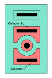
One advantage of the lateral PNP transistor: the collector can be split into two (or more) sections. The emitter current, flowing radially outward is collected by the segments according to their length at the inside. There is a small loss in gain because of the gaps, but the matching between the two collector currents is excellent.
In a CMOS process emitter and collector are usually formed by the p-type diffusion of a p-channel MOS transistor. The intervening space (the base-width) is the same as a p-channel gate, with poly-silicon on top. Connect the poly region to the PNP emitter; it will act as a static shield and have a (slight) beneficial effect.
Fig. 1-17: A split-collector lateral PNP transistor.
CMOS Transistors
It took almost 30 years after the invention of the bipolar transistor for MOS to make its appearance. Shockley (and many others) had thought of this device first, it was (or should have been) much more simple: put a plate close to the surface of silicon, connect it to a voltage and move the carriers inside the silicon electro-statically.
The problem was the surface of silicon. Here the silicon atoms are no longer neatly tied up with each other by sharing the outermost electrons. They face an entirely different material, SiO2 (or worse, some covering with unknown impurities mixed in). This material doesn't even have a crystal structure, it is amorphous.
Preliminary Edition September 2004 |
1-23 |
All rights reserved |
Camenzind: Designing Analog Chips |
Chapter 1: Devices |
In 1964 a startup, General Microelectronics, felt it had licked the problem with CMOS and brought out the first digital MOS integrated circuit. It was one of the worst products ever to hit the market: a large portion stopped working within days. The reason: there were elements with the silicon-dioxide (chiefly sodium) that carried an electric charge and could move. One day the MOS transistor was perfectly functional, the next day it was permanently turned on.
It took another few years to gain an understanding of MOS surface physics and make stable MOS transistors. Today the silicon surface is so well understood that we can deliberately place a charge into the oxide layer that stays there for years, probably even centuries. It is now the dominant integrated device, being much smaller than the bipolar transistor. (The number of MOS transistors produced every year has long surpassed the number of ants in the world. At the time of writing this book, semiconductor manufacturers produced some 500 million transistors for every person in the world per year).
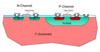
The figure
|
shows a cross-section |
|
|
of the most often |
|
|
used (n-well) process. |
|
|
There are many |
|
|
variations and |
|
|
refinements; this is |
|
|
only the basic one. |
|
|
In the gate |
|
|
area the insulating |
|
Fig. 1-18: Cross-section of an N-well CMOS process. |
||
layer (SiO2 or nitride, |
||
|
||
|
or a combination) is |
|
|
thinned down and silicon is grown on top of it. Since the insulator is amorphous, the grown silicon is not single-crystal, it consists of many small crystals which do not fit together very well (thus it is called poly-crystalline silicon or simply poly).
Next the source and drain regions are implanted, using a mask. The inside edges are masked by the gate, so they align perfectly to the gate (i.e. they are self-aligning). The device is also self-insulating: as long as the source and drain are at or above the substrate potential (usually ground), the junctions to the substrate are reverse-biased and no bulky isolation diffusion is necessary.
For the p-channel transistor the polarities for the source and drain implants are reversed and these regions are placed inside an n-type diffusion. In most applications one such n-well hosts many p-channel
Preliminary Edition September 2004 |
1-24 |
All rights reserved |