


 AT45DB642D
19. Input Test Waveforms and Measurement Levels
AC |
|
2.4V |
|
|
|
AC |
|
|
|
|
|
|
|||
DRIVING |
|
|
|
|
|
1.5V MEASUREMENT |
|
|
|
|
|
|
|||
LEVELS |
|
|
|
|
|
LEVEL |
|
0.45V |
|||||||
|
|
|
|
||||
tR, tF < 2ns (10% to 90%)
20. Output Test Load
DEVICE
UNDER
TEST
30pF
21. AC Waveforms
Six different timing waveforms are shown below. Waveform 1 shows the SCK/CLK signal being low when CS makes a high-to-low transition, and waveform 2 shows the SCK/CLK signal being high when CS makes a high-to-low transition. In both cases, output SO becomes valid while the SCK/CLK signal is still low (SCK/CLK low time is specified as tWL). Timing waveforms 1 and 2 conform to RapidS serial interface but for frequencies up to 66MHz. Waveforms 1 and 2 are compatible with SPI Mode 0 and SPI Mode 3, respectively.
Waveform 3 and waveform 4 illustrate general timing diagram for RapidS serial interface. These are similar to waveform 1 and waveform 2, except that output SO is not restricted to become valid during the tWL period. These timing waveforms are valid over the full frequency range (maximum frequency = 66MHz) of the RapidS serial case. Waveform 5 and waveform 6 are for 8-bit Rapid8 interface over the full frequency range of operation (maximum frequency = 50MHz).
21.1Waveform 1 – SPI Mode 0 Compatible (for Frequencies up to 66MHz)
|
|
|
|
tCS |
CS |
|
|
|
|
tCSS |
tWH |
tWL |
|
tCSH |
SCK/CLK |
|
|
|
|
|
tV |
|
tHO |
tDIS |
HIGH IMPEDANCE |
|
|
VALID OUT |
HIGH IMPEDANCE |
SO |
|
|
|
tSU |
tH |
SI  VALID IN
37
3542M–DFLASH–11/2012

21.2Waveform 2 – SPI Mode 3 Compatible (for Frequencies up to 66MHz)
|
|
|
tCS |
CS |
|
|
|
tCSS |
tWL |
tWH |
tCSH |
SCK/CLK |
|
|
|
tV |
|
tHO |
tDIS |
HIGH Z |
|
VALID OUT |
HIGH IMPEDANCE |
SO |
|
|
tSU |
tH |
SI |
VALID IN |
Note: To operate the device at 50MHz in SPI mode, the combined CPU setup time and rise/fall time should be less than 2ns
21.3Waveform 3 – RapidS Mode 0 (FMAX = 66MHz)
CS
tCSS |
tWH |
tWL |
SCK/CLK
tV
HIGH IMPEDANCE
SO
tSU |
tH |
|
tCS |
|
tCSH |
tHO |
tDIS |
HIGH IMPEDANCE
VALID OUT
SI |
VALID IN |
21.4Waveform 4 – RapidS Mode 3 (FMAX = 66MHz)
CS
tCSS |
tWL |
tWH |
SCK/CLK
tV |
tHO |
HIGH Z |
VALID OUT |
SO |
|
tSU |
tH |
SI |
VALID IN |
tCS |
tCSH |
tDIS |
HIGH IMPEDANCE
21.5Waveform 5 – Rapid8 Mode 0 (FMAX = 50MHz)
|
|
|
|
tCS |
CS |
|
|
|
|
tCSS |
tWH |
tWL |
|
tCSH |
SCK/CLK |
|
|
|
|
|
tV |
|
tHO |
tDIS |
HIGH IMPEDANCE |
|
|
VALID OUT |
HIGH IMPEDANCE |
I/O7 - I/O0 |
|
|
|
|
(OUTPUT) |
|
|
|
|
tSU |
tH |
I/O7 - I/O0  VALID IN

(INPUT)
38 AT45DB642D
3542M–DFLASH–11/2012

 AT45DB642D
21.6Waveform 6 – Rapid8 Mode 3 (FMAX = 50MHz)
|
|
|
tCS |
CS |
|
|
|
tCSS |
tWL |
tWH |
tCSH |
SCK/CLK |
|
|
|
tV |
|
tHO |
tDIS |
HIGH Z |
HIGH IMPEDANCE |
I/O7 - I/O0 |
VALID OUT |
(OUTPUT) |
tH |
tSU |
|
I/O7 - I/O0 |
VALID IN |
(INPUT) |
|
21.7Utilizing the RapidS Function
To take advantage of the RapidS function's ability to operate at higher clock frequencies, a full clock cycle must be used to transmit data back and forth across the serial bus. The DataFlash is designed to always clock its data out on the falling edge of the SCK signal and clock data in on the rising edge of SCK.
For full clock cycle operation to be achieved, when the DataFlash is clocking data out on the falling edge of SCK, the host controller should wait until the next falling edge of SCK to latch the data in. Similarly, the host controller should clock its data out on the rising edge of SCK in order to give the DataFlash a full clock cycle to latch the incoming data in on the next rising edge of SCK.
Figure 21-1. RapidS Mode
Slave CS
1 |
|
|
|
|
8 |
1 |
|
|
|
|
|
8 |
1 |
2 |
3 |
4 |
5 |
6 |
7 |
|
2 |
3 |
4 |
5 |
6 |
7 |
|
SCK 
MOSI
MISO
|
B |
E |
|
A |
C |
D |
|
|
MSB |
LSB |
|
|
BYTE-MOSI |
|
H |
|
|
G |
I |
|
|
F |
|
|
|
MSB |
LSB |
BYTE-SO
MOSI = Master Out, Slave In
MISO = Master In, Slave Out
The Master is the host controller and the Slave is the DataFlash
The Master always clocks data out on the rising edge of SCK and always clocks data in on the falling edge of SCK.
The Slave always clocks data out on the falling edge of SCK and always clocks data in on the rising edge of SCK.
A.Master clocks out first bit of BYTE-MOSI on the rising edge of SCK
B.Slave clocks in first bit of BYTE-MOSI on the next rising edge of SCK
C.Master clocks out second bit of BYTE-MOSI on the same rising edge of SCK
D.Last bit of BYTE-MOSI is clocked out from the Master
E.Last bit of BYTE-MOSI is clocked into the slave
F.Slave clocks out first bit of BYTE-SO
G.Master clocks in first bit of BYTE-SO
H.Slave clocks out second bit of BYTE-SO
I.Master clocks in last bit of BYTE-SO
39
3542M–DFLASH–11/2012
21.8Utilizing the Rapid8 Function
The Rapid8 functions like RapidS but with 8-bits of data instead of 1-bit. A full clock cycle must be used to transmit data back and forth across the 8-bit bus. The DataFlash is designed to always clock its data out on the falling edge of the SCK signal and clock data in on the rising edge of SCK.
For full clock cycle operation to be achieved, when the DataFlash is clocking data out on the falling edge of SCK, the host controller should wait until the next falling edge of SCK to latch the data in. Similarly, the host controller should clock its data out on the rising edge of SCK in order to give the DataFlash a full clock cycle to latch the incoming data in on the next rising edge of SCK.
Figure 21-2. Rapid8 Mode
Slave CS
1 |
2 |
3 |
4 |
5 |
6 |
7 |
|
8 |
9 |
10 |
11 |
12 |
13 |
14 |
15 |
|
|
||||||||||||||
SCK |
|
|
|
|
|
|
|
|
|
|
|
|
|
|
|
B |
|
|
tV |
|
|
D |
E |
F |
|
|
|
|
|
|
G |
C |
|
|
|
|
|
|
|
|
|
|
|||||
A |
|
|
|
|
|
|
|
|
|
|
|
|
|
|
|
I/O7-0 |
BYTE 2 |
BYTE 3 |
BYTE 4 |
|
BYTE 5 |
BYTE 6 |
|
BYTE a |
BYTE b |
BYTE c |
BYTE d |
BYTE e |
BYTE f |
BYTE g |
BYTE h |
BYTE 1 |
|
|
MOSI = Master Out, Slave In
MISO = Master In, Slave Out
The Master would be the ASIC/MCU and the Slave would be the memory device.
The Master always clocks data out on the rising edge of SCK and always clocks data in on the falling edge of SCK.
The Slave always clocks data out on the falling edge of SCK and always clocks data in on the rising edge of SCK.
A.Master clocks out BYTE 1 on the rising edge of SCK
B.Slave clocks in BYTE 1 on the next rising edge of SCK
C.Master clocks out BYTE 2 on the same rising edge of SCK
D.Slave clocks in BYTE 6 (last input byte)
E.Slave clocks out BYTE a (first output byte)
F.Master clocks in BYTE a
G.Master clocks in BYTE h (last output byte)
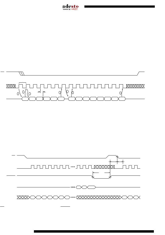
21.9Reset Timing
CS |
|
tREC |
tCSS |
SCK/CLK |
|
tRST |
|
RESET |
|
HIGH IMPEDANCE |
HIGH IMPEDANCE |
SO or I/O7 - I/O0 |
|
(OUTPUT) |
|
SI or I/O7 - I/O0 (INPUT)
Note: The CS signal should be in the high state before the RESET signal is deasserted
40 AT45DB642D
3542M–DFLASH–11/2012