

XE167x
XE166 Family Derivatives
Electrical Parameters
4.6.3External Clock Input Parameters
These parameters specify the external clock generation for the XE167. The clock can be generated in two ways:
•By connecting a crystal or ceramic resonator to pins XTAL1/XTAL2.
•By supplying an external clock signal. This clock signal can be supplied either to pin XTAL1 (core voltage domain) or to pin CLKIN1 (IO voltage domain).
If connected to CLKIN1, the input signal must reach the defined input levels VIL and VIH. In connected to XTAL1, a minimum amplitude VAX1 (peak-to-peak voltage) is sufficient for the operation of the on-chip oscillator.
Note: The given clock timing parameters (t1 … t4) are only valid for an external clock input signal.
Table 26 |
External Clock Input Characteristics |
|
|
|
||||
|
(Operating Conditions apply) |
|
|
|
|
|||
Parameter |
|
Symbol |
Limit Values |
Unit |
Note / Test |
|||
|
|
|
|
|
|
|
|
Condition |
|
|
|
|
Min. |
Typ. |
Max. |
|
|
|
|
|
|
|
|
|||
|
|
|
|
|
|
|
|
|
Input voltage range limits |
VIX1 SR |
-1.7 + |
– |
1.7 |
V |
1) |
||
|
||||||||
for signal on XTAL1 |
|
|
VDDI |
|
|
|
|
|
Input voltage (amplitude) |
VAX1 SR |
0.3 × |
– |
– |
V |
Peak-to-peak |
||
on XTAL1 |
|
|
|
V |
|
|
|
voltage2) |
|
|
|
|
DDI |
|
|
|
|
XTAL1 input current |
IIL CC |
– |
– |
±20 |
µA |
0 V < VIN < VDDI |
||
Oscillator frequency |
fOSC CC |
4 |
– |
40 |
MHz |
Clock signal |
||
|
|
|
|
4 |
– |
16 |
MHz |
Crystal or |
|
|
|
|
|
|
|
|
Resonator |
|
|
|
|
|
|
|
|
|
High time |
|
t1 SR |
6 |
– |
– |
ns |
|
|
Low time |
|
t2 SR |
6 |
– |
– |
ns |
|
|
Rise time |
|
t3 SR |
– |
8 |
8 |
ns |
|
|
Fall time |
|
t4 SR |
– |
8 |
8 |
ns |
|
|
1)Overload conditions must not occur on pin XTAL1.
2)The amplitude voltage VAX1 refers to the offset voltage VOFF. This offset voltage must be stable during the operation and the resulting voltage peaks must remain within the limits defined by VIX1.
Data Sheet |
99 |
V2.1, 2008-08 |
XE167x
XE166 Family Derivatives
Electrical Parameters
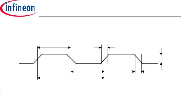
t1 |
t3 |
VOFF |
VAX1 |
|
t2 |
|
t4 |
|
tOSC = 1/fOSC |
|
MC_EXTCLOCK |
Figure 20 External Clock Drive XTAL1
Note: For crystal/resonator operation, it is strongly recommended to measure the oscillation allowance (negative resistance) in the final target system (layout) to determine the optimum parameters for oscillator operation.
Please refer to the limits specified by the crystal/resonator supplier.
Data Sheet |
100 |
V2.1, 2008-08 |
XE167x
XE166 Family Derivatives
Electrical Parameters
4.6.4External Bus Timing
The following parameters specify the behavior of the XE167 bus interface.
Table 27 |
CLKOUT Reference Signal |
|
|
|
|
||||
Parameter |
|
Symbol |
|
Limits |
Unit |
Note / Test |
|||
|
|
|
|
|
|
|
|
|
Condition |
|
|
|
|
|
Min. |
|
Max. |
|
|
|
|
|
|
|
|
|
|
||
|
|
|
|
|
|
|
|
|
|
CLKOUT cycle time |
t5 |
CC |
|
40/25/12.51) |
ns |
|
|||
CLKOUT high time |
t6 |
CC |
3 |
|
– |
ns |
|
||
CLKOUT low time |
t7 |
CC |
3 |
|
– |
ns |
|
||
CLKOUT rise time |
t8 |
CC |
– |
|
3 |
ns |
|
||
CLKOUT fall time |
t9 |
CC |
– |
|
3 |
ns |
|
||
1)The CLKOUT cycle time is influenced by the PLL jitter (given values apply to fSYS = 25/40/80 MHz). For longer periods the relative deviation decreases (see PLL deviation formula).
|
|
|
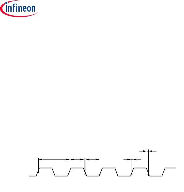
t9 |
t5 |
t6 |
t7 |
t8 |
CLKOUT |
|
|
|
|
|
|
MC_X_EBCCLKOUT |
Figure 21 CLKOUT Signal Timing
Note: The term CLKOUT refers to the reference clock output signal which is generated by selecting fSYS as the source signal for the clock output signal EXTCLK on pin
P2.8 and by enabling the high-speed clock driver on this pin.
Data Sheet |
101 |
V2.1, 2008-08 |

XE167x
XE166 Family Derivatives
Electrical Parameters
Variable Memory Cycles
External bus cycles of the XE167 are executed in five consecutive cycle phases (AB, C, D, E, F). The duration of each cycle phase is programmable (via the TCONCSx registers) to adapt the external bus cycles to the respective external module (memory, peripheral, etc.).
The duration of the access phase can optionally be controlled by the external module using the READY handshake input.
This table provides a summary of the phases and the ranges for their length.
Table 28 |
Programmable Bus Cycle Phases (see timing diagrams) |
|
|||
Bus Cycle Phase |
Parameter |
Valid Values |
Unit |
||
|
|
|
|
|
|
Address setup phase, the standard duration of this |
tpAB |
1 |
… 2 (5) |
TCS |
|
phase (1 … 2 TCS) can be extended by 0 … 3 TCS |
|
|
|
|
|
if the address window is changed |
|
|
|
|
|
|
|
|
|
|
|
Command delay phase |
tpC |
0 |
… 3 |
TCS |
|
|
|
|
|
||
Write Data setup/MUX Tristate phase |
tpD |
0 … 1 |
TCS |
||
|
|
|
|
|
|
Access phase |
|
tpE |
1 |
… 32 |
TCS |
|
|
|
|
|
|
Address/Write Data hold phase |
tpF |
0 |
… 3 |
TCS |
|
|
|
|
|
|
|
Note: The bandwidth of a parameter (from minimum to maximum value) covers the whole operating range (temperature, voltage) as well as process variations. Within a given device, however, this bandwidth is smaller than the specified range. This is also due to interdependencies between certain parameters. Some of these interdependencies are described in additional notes (see standard timing).
Data Sheet |
102 |
V2.1, 2008-08 |

XE167x
XE166 Family Derivatives
Electrical Parameters
Table 29 |
External Bus Cycle Timing for Upper Voltage Range |
|
|
||||||||
|
|
|
|
(Operating Conditions apply) |
|
|
|
|
|
||
Parameter |
|
Symbol |
|
Limits |
Unit |
Note |
|||||
|
|
|
|
|
|
|
|
|
|
|
|
|
|
|
|
|
|
|
Min. |
Typ. |
Max. |
|
|
|
|
|
|
|
|
|
|||||
Output valid delay for: |
t10 CC |
– |
|
13 |
ns |
|
|||||
|
|
|
|
|
|
|
|
|
|
|
|
RD |
, WR(L/H) |
|
|
|
|
|
|
|
|
||
Output valid delay for: |
t11 CC |
– |
|
13 |
ns |
|
|||||
BHE, ALE |
|
|
|
|
|
|
|
|
|||
Output valid delay for: |
t12 CC |
– |
|
14 |
ns |
|
|||||
A23 … A16, A15 … A0 (on P0/P1) |
|
|
|
|
|
|
|
||||
Output valid delay for: |
t13 CC |
– |
|
14 |
ns |
|
|||||
A15 … A0 (on P2/P10) |
|
|
|
|
|
|
|
||||
Output valid delay for: |
t14 CC |
– |
|
13 |
ns |
|
|||||
CS |
|
|
|
|
|
|
|
|
|||
Output valid delay for: |
t15 CC |
– |
|
14 |
ns |
|
|||||
D15 … D0 (write data, MUX-mode) |
|
|
|
|
|
|
|
||||
Output valid delay for: |
t16 CC |
– |
|
14 |
ns |
|
|||||
D15 … D0 (write data, DEMUX- |
|
|
|
|
|
|
|
||||
mode) |
|
|
|
|
|
|
|
|
|||
|
|
|
|
|
|
|
|||||
Output hold time for: |
t20 CC |
0 |
|
8 |
ns |
|
|||||
|
|
|
|
|
|
|
|
|
|
|
|
RD, |
WR(L/H) |
|
|
|
|
|
|
|
|
||
Output hold time for: |
t21 CC |
0 |
|
8 |
ns |
|
|||||
BHE, ALE |
|
|
|
|
|
|
|
|
|||
Output hold time for: |
t23 CC |
0 |
|
8 |
ns |
|
|||||
A23 … A16, A15 … A0 (on P2/P10) |
|
|
|
|
|
|
|
||||
Output hold time for: |
t24 CC |
0 |
|
8 |
ns |
|
|||||
CS |
|
|
|
|
|
|
|
|
|||
Output hold time for: |
t25 CC |
0 |
|
8 |
ns |
|
|||||
D15 … D0 (write data) |
|
|
|
|
|
|
|
||||
Input setup time for: |
t30 SR |
18 |
|
– |
ns |
|
|||||
READY, D15 … D0 (read data) |
|
|
|
|
|
|
|
||||
Input hold time for: |
t31 SR |
-4 |
|
– |
ns |
|
|||||
READY, D15 … D0 (read data)1) |
|
|
|
|
|
|
|
||||
1)Read data are latched with the same internal clock edge that triggers the address change and the rising edge of RD. Address changes before the end of RD have no impact on (demultiplexed) read cycles. Read data can change after the rising edge of RD.
Data Sheet |
103 |
V2.1, 2008-08 |

XE167x
XE166 Family Derivatives
Electrical Parameters
Table 30 |
External Bus Cycle Timing for Lower Voltage Range |
|
|
||||||||
|
|
|
|
(Operating Conditions apply) |
|
|
|
|
|
||
Parameter |
|
Symbol |
|
Limits |
Unit |
Note |
|||||
|
|
|
|
|
|
|
|
|
|
|
|
|
|
|
|
|
|
|
Min. |
Typ. |
Max. |
|
|
|
|
|
|
|
|
|
|||||
Output valid delay for: |
t10 CC |
– |
|
20 |
ns |
|
|||||
|
|
|
|
|
|
|
|
|
|
|
|
RD |
, WR(L/H) |
|
|
|
|
|
|
|
|
||
Output valid delay for: |
t11 CC |
– |
|
20 |
ns |
|
|||||
BHE, ALE |
|
|
|
|
|
|
|
|
|||
Output valid delay for: |
t12 CC |
– |
|
22 |
ns |
|
|||||
A23 … A16, A15 … A0 (on P0/P1) |
|
|
|
|
|
|
|
||||
Output valid delay for: |
t13 CC |
– |
|
22 |
ns |
|
|||||
A15 … A0 (on P2/P10) |
|
|
|
|
|
|
|
||||
Output valid delay for: |
t14 CC |
– |
|
20 |
ns |
|
|||||
CS |
|
|
|
|
|
|
|
|
|||
Output valid delay for: |
t15 CC |
– |
|
21 |
ns |
|
|||||
D15 … D0 (write data, MUX-mode) |
|
|
|
|
|
|
|
||||
Output valid delay for: |
t16 CC |
– |
|
21 |
ns |
|
|||||
D15 … D0 (write data, DEMUX- |
|
|
|
|
|
|
|
||||
mode) |
|
|
|
|
|
|
|
|
|||
|
|
|
|
|
|
|
|||||
Output hold time for: |
t20 CC |
0 |
|
10 |
ns |
|
|||||
|
|
|
|
|
|
|
|
|
|
|
|
RD, |
WR(L/H) |
|
|
|
|
|
|
|
|
||
Output hold time for: |
t21 CC |
0 |
|
10 |
ns |
|
|||||
BHE, ALE |
|
|
|
|
|
|
|
|
|||
Output hold time for: |
t23 CC |
0 |
|
10 |
ns |
|
|||||
A23 … A16, A15 … A0 (on P2/P10) |
|
|
|
|
|
|
|
||||
Output hold time for: |
t24 CC |
0 |
|
10 |
ns |
|
|||||
CS |
|
|
|
|
|
|
|
|
|||
Output hold time for: |
t25 CC |
0 |
|
10 |
ns |
|
|||||
D15 … D0 (write data) |
|
|
|
|
|
|
|
||||
Input setup time for: |
t30 SR |
29 |
|
– |
ns |
|
|||||
READY, D15 … D0 (read data) |
|
|
|
|
|
|
|
||||
Input hold time for: |
t31 SR |
-6 |
|
– |
ns |
|
|||||
READY, D15 … D0 (read data)1) |
|
|
|
|
|
|
|
||||
1)Read data are latched with the same internal clock edge that triggers the address change and the rising edge of RD. Address changes before the end of RD have no impact on (demultiplexed) read cycles. Read data can change after the rising edge of RD.
Data Sheet |
104 |
V2.1, 2008-08 |

XE167x
XE166 Family Derivatives
Electrical Parameters
tpAB |
tpC |
tpD |
tpE |
tpF |
CLKOUT |
|
|
|
|
t11 |
t21 |
|
|
|
|
|
|
|
|
ALE |
|
|
|
|
t11/t14 |
|
|
|
t24 |
A23-A16, |
|
High Address |
|
|
BHE, CSx |
|
|
||
|
|
|
t20 |
|
|
|
|
t10 |
|
|
|
|
|
|
RD |
|
|
|
|
WR(L/H) |
|
|
|
t31 |
|
|
|
|
|
t13 |
|
t23 |
t30 |
|
AD15-AD0 |
Low Address |
|
Data In |
|
(read) |
|
|
||
|
|
|
|
|
t13 |
|
t15 |
|
t25 |
AD15-AD0 |
Low Address |
|
Data Out |
|
(write) |
|
|
||
|
|
|
|
|
|
|
|
|
MC_X_EBCMUX |
Figure 22 Multiplexed Bus Cycle
Data Sheet |
105 |
V2.1, 2008-08 |

XE167x
XE166 Family Derivatives
Electrical Parameters
tpAB |
tpC |
tpD |
tpE |
tpF |
CLKOUT |
|
|
|
|
t11 |
t21 |
|
|
|
|
|
|
|
|
ALE |
|
|
|
|
t11/t14 |
|
|
|
t24 |
A23-A0, |
|
Address |
|
|
BHE, CSx |
|
|
|
|
|
|
|
t20 |
|
|
|
t10 |
|
|
|
|
|
|
|
RD |
|
|
|
|
WR(L/H) |
|
|
|
t31 |
|
|
|
|
|
|
|
|
t30 |
|
D15-D0 |
|
|
Data In |
|
(read) |
|
|
|
|
|
t16 |
|
t25 |
|
|
|
|
||
D15-D0 |
|
|
Data Out |
|
(write) |
|
|
|
|
|
|
|
|
|
|
|
|
|
MC_X_EBCDEMUX |
Figure 23 Demultiplexed Bus Cycle
Data Sheet |
106 |
V2.1, 2008-08 |

XE167x
XE166 Family Derivatives
Electrical Parameters
Bus Cycle Control with the READY Input
The duration of an external bus cycle can be controlled by the external circuit using the READY input signal. The polarity of this input signal can be selected.
Synchronous READY permits the shortest possible bus cycle but requires the input signal to be synchronous to the reference signal CLKOUT.
An asynchronous READY signal puts no timing constraints on the input signal but incurs a minimum of one waitstate due to the additional synchronization stage. The minimum duration of an asynchronous READY signal for safe synchronization is one CLKOUT period plus the input setup time.
An active READY signal can be deactivated in response to the trailing (rising) edge of the corresponding command (RD or WR).
If the next bus cycle is controlled by READY, an active READY signal must be disabled before the first valid sample point in the next bus cycle. This sample point depends on the programmed phases of the next cycle.
Data Sheet |
107 |
V2.1, 2008-08 |

XE167x
XE166 Family Derivatives
Electrical Parameters
tpD |
tpE |
tpRDY |
tpF |
|
CLKOUT |
|
|
|
|
|
t10 |
|
|
t20 |
RD, WR |
|
|
|
|
|
|
|
|
t31 |
|
|
|
t30 |
|
D15-D0 |
|
|
Data In |
|
(read) |
|
|
|
|
|
|
|
t25 |
|
|
|
|
|
|
D15-D0 |
|
Data Out |
|
|
(write) |
|
|
|
|
|
t31 |
|
t31 |
|
|
|
|
||
|
|
t30 |
t30 |
|
READY |
|
Not Rdy |
READY |
|
Synchronous |
|
|||
t31 |
|
t31 |
|
|
|
|
|
||
|
t30 |
t30 |
|
|
READY |
Not Rdy |
READY |
|
|
Asynchron. |
|
|
||
|
|
|
|
|
|
|
|
|
MC_X_EBCREADY |
Figure 24 READY Timing
Note: If the READY input is sampled inactive at the indicated sampling point (“Not Rdy”) a READY-controlled waitstate is inserted (tpRDY),
sampling the READY input active at the indicated sampling point (“Ready”) terminates the currently running bus cycle.
Note the different sampling points for synchronous and asynchronous READY.
This example uses one mandatory waitstate (see tpE) before the READY input value is used.
Data Sheet |
108 |
V2.1, 2008-08 |
XE167x
XE166 Family Derivatives
Electrical Parameters
External Bus Arbitration
If the arbitration signals are enabled, the XE167 makes its external resources available in response to an arbitration request.
Table 31 Bus Arbitration Timing for Upper Voltage Range (Operating Conditions apply)
Parameter |
|
Symbol |
|
Limits |
|
Unit |
Note |
|
|
|
|
|
Min. |
Typ. |
Max. |
|
|
|
|
|
|
|
|
|
||
Input setup time for: |
t40 SR |
18 |
|
– |
ns |
|
||
HOLD input |
|
|
|
|
|
|
|
|
Output delay rising edge for: |
t41 CC |
0 |
|
13 |
ns |
|
||
HLDA, BREQ |
|
|
|
|
|
|
|
|
Output delay falling edge for: |
t42 CC |
1 |
|
14 |
ns |
|
||
HLDA |
|
|
|
|
|
|
|
|
Table 32 |
Bus Arbitration Timing for Lower Voltage Range |
|
|
|||||
|
(Operating Conditions apply) |
|
|
|
|
|
||
|
|
|
|
|
|
|
|
|
Parameter |
|
Symbol |
|
Limits |
|
Unit |
Note |
|
|
|
|
|
|
|
|
|
|
|
|
|
|
Min. |
Typ. |
Max. |
|
|
|
|
|
|
|
|
|
||
Input setup time for: |
t40 SR |
28 |
|
– |
ns |
|
||
HOLD input |
|
|
|
|
|
|
|
|
Output delay rising edge for: |
t41 CC |
0 |
|
19 |
ns |
|
||
HLDA, BREQ |
|
|
|
|
|
|
|
|
Output delay falling edge for: |
t42 CC |
1 |
|
21 |
ns |
|
||
HLDA |
|
|
|
|
|
|
|
|
Data Sheet |
109 |
V2.1, 2008-08 |

XE167x
XE166 Family Derivatives
Electrical Parameters
CLKOUT |
|
|
t40 |
HOLD |
|
|
t42 |
HLDA |
|
BREQ |
2) |
|
|
|
t10/t14 |
CSx, RD, |
3) |
WR(L/H) |
|
Addr, Data, |
|
BHE |
|
|
1) |
|
MC_X_EBCARBREL |
Figure 25 External Bus Arbitration, Releasing the Bus
Notes
1.The XE167 completes the currently running bus cycle before granting bus access.
2.This is the first possibility for BREQ to get active.
3.The control outputs will be resistive high (pull-up) after being driven inactive (ALE will be low).
Data Sheet |
110 |
V2.1, 2008-08 |

XE167x
XE166 Family Derivatives
Electrical Parameters
|
3) |
CLKOUT |
|
|
t40 |
HOLD |
|
|
t41 |
HLDA |
|
|
t41 |
BREQ |
1) |
|
|
|
t10/t14 |
CSx, RD, |
2) |
WR(L/H) |
t11/t12/t13/t15/t16 |
|
|
Addr, Data, |
|
BHE |
|
|
MC_X_EBCARBREG |
Figure 26 External Bus Arbitration, Regaining the Bus
Notes
1.This is the last chance for BREQ to trigger the indicated regain sequence.
Even if BREQ is activated earlier, the regain sequence is initiated by HOLD going high. Please note that HOLD may also be deactivated without the XE167 requesting the bus.
2.The control outputs will be resistive high (pull-up) before being driven inactive (ALE will be low).
3.The next XE167-driven bus cycle may start here.
Data Sheet |
111 |
V2.1, 2008-08 |