

Dressel.Gruner.Electrodynamics of Solids.2003
.pdf148 |
6 Semiconductors |
Here N is the density of electrons in the valence band and m is the mass of the charge carriers, which may be replaced by the bandmass. The verification of the sum rule is somewhat more involved for 1/τ comparable to ω0, and in the limit 1/τ ω0 we recover the sum rule as derived for the Drude model.
6.2Direct transitions
6.2.1General considerations on energy bands
Within the framework of the band theory of solids, insulators and semiconductors have a full band at zero temperature, called the valence band, separated by a single-particle gap Eg from the conduction band, which at T = 0 is empty. Because there is a full band and a gap, the static electrical conductivity σdc(T = 0) = 0, and optical absorption occurs only at finite frequencies. The valence and conduction bands are sketched in Fig. 6.8a in the so-called reduced Brillouin zone representation with two different dispersion relations displayed in the upper and lower parts of the figure. In general, excitation of an electron from the valence band to the conduction band (indicated by subscripts c and v, respectively) leads to an extra electron with momentum k in the conduction band, leaving a hole with momentum k behind in the valence band. In a crystal, momentum conservation requires that
k = k + K |
(6.2.1) |
where K is the reciprocal lattice vector. Neglecting umklapp processes, we consider only vertical direct transitions, for which k = k. Such transitions obey
hω = Ec(k ) − Ev(k) |
(6.2.2) |
¯ |
|
due to the energy conservation, and are indicated in Fig. 6.8 by d. Of course these transitions appear to be vertical in this reduced zone representation where the dispersions at the higher Brillouin zone are folded back to the first zone; in the extended zone representation the electron gains the momentum K from the crystal lattice, in a fashion similar to that which leads to the band structure itself.
Processes where momentum is absorbed by the lattice vibrations during the creation of electrons and holes, and
k = k + P , |
(6.2.3) |
with P the wavevector of the phonon involved, are also possible, and we refer to these processes as indirect transitions. With both direct and indirect transitions of importance, Fig. 6.8 suggests different scenarios for the onset of optical absorptions. In Fig. 6.8a, the lowest energy transition is a direct transition, and will dominate the onset of optical absorption. In contrast, the situation shown in

150 |
6 Semiconductors |
Fig. 6.8b is an indirect transition for which
hω = Ec(k ) − Ev(k) ± hωP , |
(6.2.4) |
|
¯ |
¯ |
|
where ωP is the frequency of the relevant phonon which determines the onset of optical absorption.
First let us consider direct transitions from the top of the valence band to the bottom of the conduction band as shown in Fig. 6.8a. In the simplest case these transitions determine the optical properties near to the bandgap. As expected, the solution of the problem involves two ingredients: the transition matrix element between the conduction and valence bands, and the density of states of these bands. As far as the transition rate is concerned, knowing the solution of the one-electron Schrodinger¨ equation at these extreme points in the Brillouin zone, it is possible to obtain solutions in their immediate neighborhood by treating the scalar product k · p as a perturbation (see Appendix C) [Jon73, Woo72].
Some assumptions will be made concerning the density of states. We assume the energy band to be parabolic near the absorption edge, and the dispersion relations are given by
|
|
|
h2k2 |
|
|
|
|
|
|
h2k2 |
|
|
E |
v |
= − |
¯ |
and |
E |
c |
= E |
g |
+ |
¯ |
, |
(6.2.5) |
|
2mv |
|
|
|
2mc |
|
|
where Eg is the single-particle gap, and mv and mc refer to the bandmass in the valence and conduction bands, respectively. h¯ k is measured from the momentum which corresponds to the smallest gap value k0 in Fig. 6.8, and zero energy corresponds to the top of the valence band.
6.2.2 Transition rate and energy absorption for direct transitions
We first discuss the transition probabilities and absorption rates; subsequently the absorption rate is related to the complex conductivity and complex dielectric constant. We follow the procedure used in the previous treatment of the electrodynamics of metals.
The states in the valence and conduction bands are described by Bloch wavefunctions
l |
= |
−1/2 exp{ik · r}ul (k) |
(6.2.6a) |
l |
= |
−1/2 exp{ik · r}ul (k ) . |
(6.2.6b) |
We use the indices l and l to indicate that this applies generally to any interband transition; refers to the volume element over which the integration is carried out. The Hamiltonian which describes the interaction of the electromagnetic field with
6.2 Direct transitions |
151 |
the electronic states is given by Eq. (4.3.24), which, if p = −ih¯ , can be rewritten as
|
ieh |
|
|
|
|
H = − |
¯ |
(A |
· + · |
A) . |
(6.2.7) |
2mc |
|
|
|
We assume, for the sake of generality, that the vector has the following momentum dependence
A(q) = A exp{iq · r} ,
and we neglect the frequency dependence for the moment. The matrix element of the transition is
H |
|
= |
l |
− |
ieh |
{ |
|
· } · + · |
{ |
|
· |
} |
|
|
|
2mc |
|
|
|
||||||||||
ll |
(r) |
|
|
|
¯ |
(A exp |
iq |
r |
A exp |
iq |
|
r |
) |
l dr . |
(6.2.8) By substituting the Bloch functions for the valence and conduction bands, the transition matrix element becomes
Hll |
|
= − |
ieh |
1 |
|
l |
|
|
· |
|
|
+ |
|
|
|
|
· |
|
|
{ |
|
|
|
+ |
|
|
− |
|
· |
} |
|
|
|
|
|
|||||
|
2mc |
|
|
|
|
|
|
|
|
|
|
|
|
|
|
|
|
|
|
|
||||||||||||||||||||
int |
(r) |
|
¯ |
|
|
|
u |
|
A |
|
ul |
|
|
|
iul |
A |
|
k |
|
exp |
i(k |
|
|
q |
|
|
k) |
|
r |
|
dr |
|
(6.2.9) |
|||||||
|
|
|
|
|
|
|
|
|
|
|
|
|
|
|
|
|
||||||||||||||||||||||||
|
|
= − |
ieh |
1 |
n |
|
{ |
i(k |
+ |
q |
− |
k) |
· |
Rn |
|
l |
|
A |
· |
ul |
|
+ |
|
|
A |
· |
k |
|
dr |
|||||||||||
|
|
2mc |
|
|
} |
|
|
|
||||||||||||||||||||||||||||||||
|
|
|
¯ |
|
|
|
exp |
|
|
|
|
|
|
u |
|
|
|
|
|
|
iul |
|
|
|||||||||||||||||
|
|
|
|
|
|
|
|
|
|
|
|
|
|
|
|
|
|
|
|
|
|
|
|
|
|
|
|
|
|
|
|
|
|
|
|
|
|
|||
with m the electron mass and the unit cell volume. For a periodic crystal structure
exp{i(k + q − k) · r} = exp{i(k + q − k) · (Rn + r )} ,
where Rn is the position of the nth unit cell. Here
exp{i(k + q − k) · Rn } ≈ 0
n
unless (k + q − k) = K, where K is a reciprocal lattice vector. In the reduced zone scheme, we can take K = 0, so that k = k + q. For direct or vertical transitions k = k , and therefore q = 0. Thus we obtain
Hll |
= − |
ieh 1 |
|
l |
· |
|
|
+ |
|
· |
|
|
|
||
2mc |
|
|
|
|
|||||||||||
int(r) |
|
¯ |
|
|
|
u (k)[A |
|
ul |
(k) |
|
iA |
|
kul |
(k)] dr . |
(6.2.10) |
For a pure semiconductor the second term is zero due to the orthogonality of the Bloch functions, and transitions associated with this matrix element are forbidden. Of course this restriction can be lifted by scattering processes (due to impurity scattering for example), and the optical properties when this occurs will be discussed later. In the majority of cases, the first term in the brackets dominates
152 |
6 Semiconductors |
the absorption process, and we call the situation when this term is finite allowed transition [Coh88, Rid93].
By substituting the momentum operator
|
|
= |
| |
| |
|
= − |
ih |
|
l |
|
|
|
|
|
|
|
|||||||
pl |
l |
|
kl |
p |
kl |
|
¯ |
|
u |
ul dr , |
(6.2.11) |
which is sometimes called the electric dipole transition matrix element, we obtain
Hlintl = mce A · pl l ,
neglecting the forbidden transitions for the moment. The transition rate of an electron from state |kl to state |kl can now be calculated by using Fermi’s golden rule:
Wl l |
= |
Wll |
= |
(2π/h) |
Hllint |
2δ |
l l |
hω |
} |
. |
(6.2.12) |
→ |
|
¯ | |
| |
|
{E |
− ¯ |
|
|
Here we consider the number of transitions per unit time. These lead to absorption, and are therefore related to the real part of the conductivity σ1(ω), which will be evaluated shortly. Subsequently we have to perform a Kramers–Kronig transformation to evaluate the imaginary part. To obtain the transition rate from the initial band l to band l , we have to integrate over all allowed values of k, where we have 1/(2π )3 states per unit volume in each spin direction:
|
π 2 |
2 |
|
|
|
|
|
|
||
Wll (ω) = |
e |
|
|
BZ |A · pl l |2δ{h¯ ω − El l } dk , |
(6.2.13) |
|||||
2m2hc2 |
(2π )3 |
|||||||||
|
¯ |
|
|
|
|
|
|
|
|
|
where the energy difference |
l |
|
|
l |
l l |
hωl l . |
|
|||
|
|
|
|
E |
− E = E |
= ¯ |
|
|||
Using the relation we derived in Section 2.3.1 for the absorbed power, |
|
|||||||||
|
P |
= |
σ1 |
|
E2 |
hωWl l , |
|
|||
|
|
|
|
|
|
= ¯ |
|
|
||
the absorption coefficient, which according to Eq. (2.3.26) is defined as the power absorbed in the unit volume divided by the energy density times the energy velocity, becomes
|
|
4π hωl l Wl l (ω) |
|
|
|
αl l (ω) |
= |
¯ |
|
. |
(6.2.14) |
|
nc E2 |
|
|
||
Substituting Eq. (6.2.13) into Eq. (6.2.14) we obtain our final result: the absorption coefficient corresponding to the transition from state l to state l ,
αl l (ω) = |
e2 |
BZ |pl l |2δ{h¯ ω − h¯ ωl l } dk . |
(6.2.15) |
π ncm2ω |
As discussed earlier, αl l (ω) is related to the imaginary part of the refractive index. Note that in general n = n(ω), but with Eq. (2.3.26) (the expression which relates the refractive index to the conductivity) we can immediately write down

6.3 Band structure effects and van Hove singularities |
153 |
the contribution of the transition rate between the l and l bands to the conductivity as
|
c |
(6.2.16) |
σ1(ω) = |
4π αl l (ω)n(ω) . |
The conductivity σ1(ω) is proportional to the transition rate times the real part of the refractive index – which itself has to be evaluated in a selfconsistent way. Hence, the procedure is not trivial as n(ω) depends on both σ1(ω) and σ2(ω).
Next we consider the electrodynamics of semiconductors by starting from a somewhat different point. In Eq. (4.3.33) we arrived at a general formalism for the transverse dielectric constant which includes both intraband and interband transitions. The total complex dielectric constant is the sum of both processes:
ˆ(q, ω) = ˆinter(q, ω) + ˆintra(q, ω) . |
(6.2.17) |
In Chapter 5, the discussion focused on the dielectric response due to intraband excitations; these are particularly important for metals. Now we discuss interband transitions due to direct excitations across the bandgap Eg of the semiconductor. We can split the dielectric constant into its real and imaginary parts following Eqs (4.3.34b) and (4.3.34a), and in the q = 0 limit we arrive at
|
|
|
|
4π e2 |
|
|
f |
0( |
|
) |
|
|
|
|
|
|
|
1 |
|
|
|
|
|
|
||||
1 |
(ω) = 1 − |
|
|
|
|
|
|
|
|
Ekl |
|
|
|
|
|
|
|
|
|pl l |2 |
(6.2.18a) |
||||||||
|
m2 |
k l,l |
kl |
|
k,l |
( |
kl |
− E |
k,l )2 |
|
h2ω2 |
|||||||||||||||||
|
|
|
4π 2 |
|
e2 |
|
|
E |
− E |
E |
|
|
− ¯ |
|
|
|
|
|||||||||||
2 |
(ω) |
= |
|
|
f 0( |
kl )δ |
kl |
− E |
kl |
|
hω |
} | |
pl l |
| |
2 |
, |
(6.2.18b) |
|||||||||||
|
|
|
|
|
|
|
||||||||||||||||||||||
|
|
|
|
|
|
|
|
|
||||||||||||||||||||
|
|
ω2m2 |
k l=l |
|
E |
|
|
{E |
|
− ¯ |
|
|
|
|
||||||||||||||
where we have used Eq. (6.2.11). At T = 0 the Fermi distribution becomes a step function; after replacing the sum over k by an integral over a surface of constant energy, the imaginary part of the dielectric constant has the form
2(ω) = |
4π 2e2 |
l=l |
2 |
h¯ ω=El l |
δ {Ekl − Ekl − h¯ ω} |pl l |2 dk . |
(6.2.19) |
ω2m2 |
(2π )3 |
|||||
|
|
|
|
|
|
|
This expression can be cast into a form identical to Eq. (6.2.15) by noting that the energy difference Ekl − Ekl = h¯ ωll , using the relationships 2 = 1 + 4π σ1/ω and α = 4π σ1/(nc) between the dielectric constant, the conductivity, and the absorption coefficient.
6.3 Band structure effects and van Hove singularities
Besides the matrix element of the transition, the dielectric properties of semiconductors are determined by the electronic density in the valence and in the

154 |
6 Semiconductors |
conduction bands. For a band l with the dispersion relation kEl (k) the so-called density of states (DOS) is given by
Dl (E) dE = |
2 |
El (k)=const. |
dSE |
dE |
(6.3.1) |
|
(2π )3 |
| kEl (k)| |
|
||||
with the factor of 2 referring to the two spin directions. The expression gets most contributions from states where the dispersion is flat, and kEl (k) is small. For direct optical transitions between two bands with an energy difference El l = El − El , however, a different density is relevant; this is the so-called combined or joint density of states, which is defined as
Dl l (h¯ ω) = |
2 |
BZ δ{El (k) − El (k) − h¯ ω} dk |
|
||
|
|
||||
(2π )3 |
|
||||
= |
2 |
h¯ ω=El l |
dSE |
(6.3.2) |
|
(2π )3 |
| k[El (k) − El (k)]| |
. |
|||
The critical points, where the denominator in the expression becomes zero,
|
k[ l (k) |
l (k)] |
k l (k) |
k l (k) |
= |
0 , |
(6.3.3) |
E |
− E |
= E |
− E |
|
|
are called van Hove singularities in the joint density of states. This is the case for photon energies h¯ ωl l for which the two energy bands separated by El l are parallel at a particular k value.
Rewriting the integral in Eq. (6.2.19), we immediately see that the imaginary part of the dielectric constant is directly proportional to the joint density of states, and
|
|
4π e2 |
|
|
2 |
l,l l l =const. |
|
|
dS |
|
|
|
|
2(ω) = |
|
|
|
|
|
|
E |
l (k)] |
|
|pl l |2 |
|||
|
m2ω2 (2π )3 |
| |
k[ l (k) |
| |
|||||||||
|
|
|
|
|
|
|
E |
E |
− E |
|
|||
= |
|
2π e |
|
2 |
Dl l (h¯ ω)|pl l |2 |
. |
|
|
|
(6.3.4) |
|||
mω |
l,l |
|
|
|
|||||||||
|
|
|
|
|
|
|
|
|
|
|
|
|
|
The message of this expression is clear: the critical points – where the joint density of states peaks – determine the prominent structures in the imaginary part of the dielectric constant 2(ω) and thus of the absorption coefficient.
Next we evaluate the optical parameters of semiconductors using previously derived expressions.
6.3.1 The dielectric constant below the bandgap
For a semiconductor in the absence of interactions, and also in the absence of lattice imperfections, at T = 0, there is no absorption for energies smaller than

6.3 Band structure effects and van Hove singularities |
155 |
the bandgap. The conductivity σ1, and therefore the absorption coefficient, are zero, but the dielectric constant 1 is finite, positive, and it is solely responsible for the optical properties in this regime. In the static limit, ω → 0, 1 can be calculated if the details of the dispersion relations of the valence and conduction bands are known. Let us first assume that we have two, infinitely narrow, bands with the maximum of the valence band at the same k position as the minimum
of the conduction band, separated by the energy Eg |
= hωg. In this case, from |
|||||||||||||
Eq. (6.1.11) we find |
|
|
|
|
|
|
|
|
|
|
¯ |
|
|
|
|
|
|
|
|
|
|
|
|
|
|
|
|
|
|
|
|
|
|
|
|
4π N e2 |
|
|
|
ωp |
|
2 |
||
|
= |
0) |
= |
1 |
+ |
1 |
+ |
(6.3.5) |
||||||
1(ω |
mωg2 = |
ωg |
||||||||||||
|
|
|
|
|
|
|
|
|
|
|||||
by virtue of the sum rule which is #l fl = 1. An identical result can be derived by starting from Eq. (6.2.19) and utilizing the Kramers–Kronig relation (3.2.31)
1 |
(ω = 0) = 1 + π 0 ∞ |
2ω . |
|
|
2 |
|
(ω) |
This also indicates that 1(ω = 0) can, in general, be cast into the form of
1(ω = 0) = 1 + C |
ωg |
2 |
(6.3.6) |
||
, |
|||||
|
|
ωp |
|
|
|
where C is a numerical constant less than unity which depends on the details of the joint density of states.
6.3.2 Absorption near to the band edge
If the valence band maximum and the conduction band minimum in a semiconductor have the same wavevector k, as shown in Fig. 6.8a, the lowest energy absorption corresponds to vertical, so-called direct, transitions. Near to the band edge, for a
photon energy E = hω ≥ Eg, the dispersion relations of the valence and conduction |
|||||||||||
¯ |
|
|
|
|
|
|
|
|
|
|
|
bands are given by Eqs (6.2.5), and we obtain |
|
|
|
|
|
|
|
||||
|
h2 |
1 |
1 |
k2 |
|
h2k2 |
|
||||
El (k)−El (k) = Ec(k)−Ev(k) = Eg + |
¯2 |
|
|
+ |
|
= Eg + |
¯2µ |
, (6.3.7) |
|||
mc |
mv |
||||||||||
where |
|
|
|
|
|
|
|
|
|
||
µ = |
mcmv |
|
|
|
|
|
|
(6.3.8) |
|||
mc + mv |
|
|
|
|
|||||||
is the reduced electron–hole mass. The analytical behavior of the joint density of states Dcv(h¯ ω) near a singularity may be found by expanding Ec(k) − Ev(k) in a Taylor series around the critical point of energy difference Ek (k0).
156 |
6 Semiconductors |
First let us consider the three-dimensional case. For simplicity we assume isotropic effective masses mv and mc in the valence and conduction bands. Consequently
Ec(k) − Ev(k) = Eg + (h2 |
/2µ)|k − k0|2 . |
(6.3.9) |
¯ |
|
|
Such an expression should be appropriate close to k0, the momentum for which the band extrema occur. The joint density of states at the absorption edge can now be calculated by Eq. (6.3.2), and we obtain
|
1 |
2µ |
|
3/2 |
|
|
|
|
|
|
|||
Dcv(h¯ ω) = |
|
|
|
|
(h¯ ω − Eg)1/2 |
(6.3.10) |
2π 2 |
h2 |
|||||
|
|
¯ |
|
|
|
|
for h¯ ω > Eg. This term determines the form of the absorption, and also 2(ω) (or accordingly σ1(ω)) in the vicinity of the bandgap. For photon energies below the gap, 2(ω) = 0, i.e. the material is transparent. Substituting Eq. (6.3.10) into Eq. (6.3.4), we obtain for energies larger than the gap h¯ ω > Eg
|
2e2 |
2µ |
|
3/2 |
|
|
|
|
|
|
|||
2(ω) = |
|
|
|
|
|pcv|2(h¯ ω − Eg)1/2 . |
(6.3.11) |
m2ω2 |
h2 |
|||||
|
|
¯ |
|
|
|
|
Note that m is the mass of the charge carriers which are excited; this mass, but also the reduced electron–hole mass µ, enters into the expression of the dielectric constant. The relation for the real part of the dielectric constant 1(ω) can be obtained by applying the Kramers–Kronig relation (3.2.12a); and we find
|
2e2 |
2µ |
|
3/2 |
|
|
|
|
|
|
|
|
|
|
|||
1(ω) = 1 + |
|
|
|
|
|pcv |
|2 |
|
|
m2ω2 |
h2 |
|
|
|||||
|
|
¯ |
|
|
|
|
|
|
× 2Eg − Eg1/2(Eg + h¯ ω)1/2 − Eg1/2(Eg − h¯ ω)1/2 {Eg − h¯ ω} |
(6.3.12) |
|||||||
with the Heaviside step function |
0 |
|
|
|||||
|
|
{x − x } = |
if x < x . |
|
||||
|
|
|
|
|
|
1 |
if x > x |
|
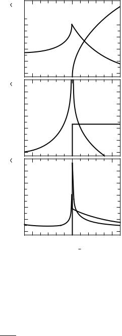
Equation (6.3.12) holds in the vicinity of the bandgap. Due to the square root dependence of 2(ω) above the energy gap, the real part of the dielectric constant1(ω) displays a maximum at ωg = Eg/h¯ and falls off as (Eg −h¯ ω)1/2 at frequencies right below the gap. Both 1(ω) and 2(ω) are displayed in Fig. 6.9. The frequency dependence of the dielectric constant leads to a characteristic behavior of the reflectivity R(ω) in the frequency range of the bandgap as displayed in Fig. 6.10; most remarkable is the peak in the reflectivity at the gap frequency ωg.
For crystals, in which the energy depends only on two components of the wavevector k, say ky and kz , the expression of the two-dimensional joint density of
 (a)
(a)