

Furber S.ARM system-on-chip architecture.2000
.pdf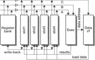
390 |
The AMULET Asynchronous ARM Processors |
Figure 14.11 The AMULETS reorder buffer organization.
AMULETS |
The performance characteristics of AMULET3 are summarized in Table 14.4. It can |
|||||
performance |
be seen that the objective of achieving comparability with the ARM9TDMI on the |
|||||
|
same process has been met. |
|
|
|
||
|
AMULET3 has been used as the processing core in the DRACO telecommunica- |
|||||
|
tions controller; this is the subject of the next section. |
|||||
|
Table 14.4 AMULET3 characteristics. |
|
|
|||
|
|
|
|
|
|
|
Process |
0.35 urn |
Transistors |
113,000 |
MIPS |
120 |
|
Metal layers |
3 |
Core area |
3mm2 |
Power |
154mW |
|
Vdd |
3.3V Clock |
none MIPS/W |
780 |
|
||
|
|
|
|
|
|
|
14.6The DRACO telecommunications controller
The DRACO (DECT Radio Communications Controller) chip is the first commercial design based on AMULET technology; it uses the AMULET3H self-timed processing subsystem described later in this section as its compute and control engine.
DRACO was developed in collaboration between Hagenuk GmbH (who designed the clocked telecommunications peripherals) and the University of Manchester (who were responsible for the AMULETS H subsystem) with funding from the European Union.
392 |
The AMULET Asynchronous ARM Processors |
•an ISDN-DECT synchronizer phase-locked loop avoids bit loss in data transfers between the ISDN and DECT clock domains;
•the clock system has power-down features.
In addition, the self-timed AMULET3H processing subsystem incorporates:
•a 100 MIPS AMULET3 32-bit processor that implements ARM architecture v4T (including the Thumb 16-bit compressed instruction set) with debug hardware;
•8 Kbytes of dual-port high-speed RAM (local to the processor);
•a self-timed on-chip bus with a bridge to the synchronous on-chip bus that con nects the synchronous peripherals;
•a 32-channel DMA controller;
•16 Kbytes of ROM holding standard telecommunications application software;
•an asynchronous event driven load module that holds the processor in zero-power wait mode while an analogue-to-digital conversion completes, thereby synchro nizing the software to external data rates;
•a programmable external memory interface that supports the direct connection of SRAM, DRAM and flash memory;
•an on-chip reference delay line calibrated by software to control off-chip memory access timings.
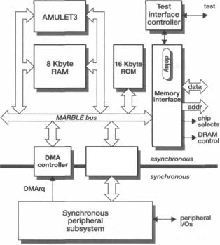
AMULET3H |
AMULET3H is a subsystem based around an AMULET3 core that forms an asyn- |
|
|
chronous 'island' at the heart of the DRACO telecommunications controller in |
|
|
which it is interfaced to a range of synchronous peripheral controllers. To reap the |
|
|
benefits of asynchronous operation the core must have access to some memory that |
|
|
operates asynchronously, and there are significant electromagnetic compatibility |
|
|
benefits in having off-chip memory also operate asynchronously. |
|
MARBLE on- |
The organization of the asynchronous subsystem is illustrated in Figure 14.12 on |
|
Chip bus |
page 393. The AMULET3 core is connected directly to a dual-ported RAM (dis- |
|
|
cussed further below) and then to the MARBLE on-chip bus. MARBLE is similar |
|
|
in concept to ARM's AMBA bus, the major difference being that it does not use a |
|
|
clock signal. Its transfer mechanism is based around a split transaction primitive. |
|
|
|
System components other than the local RAM are accessed via the MARBLE |
|
bus. These include on-chip ROM, a DMA controller, a bridge to the synchronous bus |
|
|
where the application-specific peripheral controllers reside, and an interface to exter- |
|
|
nal memory. |
|
External memory |
The external memory interface presents a conventional set of signals for |
|
|
|
off-chip |
interface |
devices. It is similar to the AMULET2e interface (see Section 14.4 on page 384), |
|
|
being highly configurable and using a reference delay to time external accesses. |
|
The DRACO telecommunications controller |
393 |
Synchronous peripheral interface
|
Figure 14.12 The AMULET3H asynchronous subsystem. |
|
Instead of using an off-chip reference delay, however, AMULETS H has an on-chip |
|
delay which can be calibrated by software against a timing reference, perhaps using |
|
a timer/counter in the synchronous peripheral subsystem for this purpose. |
|
Off-chip DRAM is supported directly, as are conventional ROM, SRAM and |
|
memory mapped peripheral devices. |
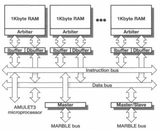
AMULET3H |
The AMULETS processor core has separate address and data buses for instruction |
memory |
and data memory accesses. This would normally require separate instruction and |
Organization |
data memories; RISC systems frequently employ a 'modified Harvard' architecture |
|
where there are separate instruction and data caches with a unified main memory. |
|
The AMULET3H controller employs direct-mapped RAM rather than cache |
|
memory as this is more cost-effective and has more deterministic behaviour for real- |
|
time applications. It also avoids separate instruction and data memories (and the asso- |
|
ciated difficulties of keeping them coherent) through the use of a dual-ported memory |
|
structure (see Figure 14.13 on page 394). Dual-porting the memory at the individual |
|
bit level would be too costly, so instead the memory is divided into eight 1 Kbyte |
|
blocks, each of which has two ports which are arbitrated internally. When concurrent |
|
data and instruction accesses are to different RAM blocks, each can proceed |
The DRACO telecommunications controller |
395 |
AMULET3H |
The simulated performance characteristics of the AMULET3H subsystem are sum- |
|||||
performance |
marized in Table 14.5. (The transistor count, area and power figures are for the |
|||||
|
asynchronous subsystem only. Overall the DRACO die is 7.8 x 7.3 mm.) The maxi- |
|||||
|
mum system performance is slightly lower than that of the AMULET3 core |
|||||
|
(reported in Table 14.4 on page 390) since the on-chip RAM cannot supply the |
|||||
|
processor's peak instruction bandwidth requirement. The system power-efficiency is |
|||||
|
lower than that of the processor alone since the memory system power is now |
|||||
|
included as well as the power consumed by the processor core itself. |
|||||
|
Table 14.5 |
AMULET3H characteristics. |
|
|
||
|
|
|
|
|
|
|
Process |
0.35 urn |
Transistors |
825,000 |
MIPS |
100 |
|
Metal layers |
3 |
Core area |
21mm2 |
Power |
215 mW |
|
Vdd |
3.3V |
Clock |
none MIPSAV |
465 |
|
|
|
|
|
|
|
|
|
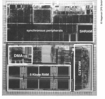
Figure 14.14 DRACO die plot.
It can be seen that the AMULET3H subsystem is competitive with the equivalent clocked ARM systems in terms of performance and power-efficiency. It has the
396 The AMULET Asynchronous ARM Processors
|
advantages of better electromagnetic interference and system power management |
|
properties. Against these advantages must be weighed the present shortcomings in the |
|
available tool support for asynchronous design. |
DRACO |
The DRACO chip can be used in a number of telecommunications applications. A |
applications |
typical application is a combined ISDN terminal and DECT base-station which |
|
would enable a number of users to communicate with each other using cordless |
|
DECT handsets and to connect to the telecommunications network via the ISDN |
|
line or a cordless ISDN network terminator. The principal target market for the chip |
|
is in cordless DECT data applications. |
DRACO silicon |
A plot of the DRACO silicon layout is shown in Figure 14.14 on page 395. The |
|
AMULET3H asynchronous subsystem occupies the bottom half of the core area; |
|
the synchronous telecommunications peripherals occupy the top half. First silicon |
|
was fabricated early in 2000. |
14.7A self-timed future?
Although AMULET3 will be used commercially the AMULET programme has, so far, been primarily of a research nature, and there is no immediate prospect of the AMULET cores replacing the clocked ARM cores in widespread use. However, there is a resurgence of world-wide interest in the potential of asynchronous design styles to save power, to improve electromagnetic compatibility, and to offer a more modular approach to the design of computing hardware.
The power savings which result from removing the global clock, leaving each subsystem to perform its own timing functions whenever it has useful work to perform, are clear in theory but there are few demonstrations that the benefits can be realized in practice with circuits of sufficient complexity to be commercially interesting. The AMULET research is aimed directly at adding to the body of convincing demonstrations of the merits of asynchronous technology.
An obstacle to the widespread adoption of self-timed design styles is the knowledge-base of the existing design community. Most 1C designers have been trained to have a strong aversion to asynchronous circuits because of the difficulties that were experienced by the designers of some early asynchronous computers. These difficulties resulted from an undisciplined approach to self-timed design, and modern developments offer asynchronous design frameworks which overcome most of the problems inherent in what is, admittedly, a more anarchic approach to logic design than that offered within the clocked framework.
Example and exercises |
397 |
|
The next few years will tell whether or not AMULET and similar developments |
|
around the world can demonstrate the sort of advantages that will cause designers to |
|
throw away most of their past education and learn a new way to perform their duties. |
AMULET |
AMULET 1 was developed using European Community funding within the Open |
Support |
Microprocessor systems Initiative - Microprocessor Architecture Project (OMI- |
|
MAP). AMULET2 was developed within the Open Microprocessor systems Initia- |
|
tive - Deeply Embedded ARM (OMI-DE/ARM) project. The development of |
|
AMULETS and DRACO was supported primarily within the European Union |
|
funded OMI-DE2 and OMI-ATOM projects. Aspects of the work have benefited |
|
from support from the UK government through the Engineering and Physical Sci- |
|
ences Research Council (EPSRC) in the form of a PhD studentships and the tools |
|
development funded under ROPA grant GR/K61913. |
|
The work also received support in various forms from ARM Limited, GEC Plessey |
|
Semiconductors (now part of MITEL) and VLSI Technology, Inc. Tools from Com- |
|
pass Design Automation (now part of Avant!) were important to the success of both |
|
projects, and TimeMill from EPIC Design Technology, Inc. (now part of Synopsys) |
|
was vital to the accurate modelling of AMULET2 and AMULETS. |
14.8Example and exercises
Example 14.1 |
Summarize the advantages and disadvantages of self-timed design. |
|
The advantages discussed here are: |
|
• improved electromagnetic compatibility (EMC); |
|
• improved power-efficiency; |
|
• improved design modularity; |
|
• the removal of the clock-skew problem; |
|
• the potential for typical rather than worst-case performance. |
|
The disadvantages are: |
|
• the unavailability of design tools for self-timed design; |
|
• the lack of designer experience; |
|
• an aversion to self-timed techniques has been encouraged in design education; |
|
• there is a lack of commercial-scale demonstrations of the above-claimed advantages. |
|
In general it is still a high-risk option to pursue a self-timed solution to a design |
|
problem, and the lack of tools can make it very labour intensive. |
398 The AMULET Asynchronous ARM Processors
Exercise 14.1.1 |
Estimate the effect on the performance of both clocked and self-timed processors of |
|
memory conflicts when the processor core has separate instruction and data ports |
|
both of which are connected to a single dual-port memory. Assume the memory is |
|
constructed from eight arbitrated segments similar to the AMULET3H memory but |
|
without the line buffers (see "AMULET3H memory organization" on page 393). |
|
You can assume that the processor fetches instructions continuously and requires |
|
about one data memory access for every two instructions. The instruction and data |
|
accesses from the clocked processor will be synchronized (by the clock!), so every |
|
time contention arises one of the two accesses will be stalled for one cycle. The asyn- |
|
chronous processor has no such sychronization so the two accesses have random rela- |
|
tive timing and the stall will be for whatever proportion of the first contending access |
|
time remains when the second contending access is requested. |
Exercise 14.1.2 |
Estimate the effect on performance of the instruction and data line buffers in the |
|
AMULET3H memory system. Make the same assumptions as in the previous exercise. |