

Furber S.ARM system-on-chip architecture.2000
.pdfThe Strong ARM SA-110 |
329 |
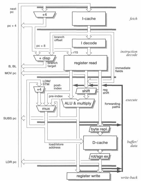
tional logic functions are fitted within their respective pipeline stages and do not add to the pipeline depth. The pipeline stages are:
1.Instruction fetch (from the instruction cache).
2.Instruction decode and register read; branch target calculation and execution.
3.Shift and ALU operation, including data transfer memory address calculation.
4.Data cache access.
5.Result write-back to register file.
The organization of the major pipeline components is illustrated in Figure 12.8 on page 330. The shaded bars delimit the pipeline stages and data which passes across these bars will be latched at the crossing point. Data which feeds around the end of a bar is being passed back or forward across pipeline stages, for example:
•The register forwarding paths which pass intermediate results on to following instructions to avoid a register interlock stall caused by a read-after-write hazard.
•The PC path which forwards pc + 4 from the fetch stage of the next instruction, giving pc + 8 for the current instruction, to be used as r15 and in the branch target calculation.
Pipeline features |
Of particular note in this pipeline structure are: |
•The need for three register read ports to enable register-controlled shifts and store with base plus index addressing to issue in one cycle.
•The need for two register write ports to allow load with auto-index to issue in one cycle.
•The address incrementer in the execute stage to support load and store multiple instructions.
•The large number of sources for the next PC value.
This last point reflects the many ways the ARM architecture allows the PC to be modified as a result of its visibility as r15 in the register bank.
PC modification The most common source of the next PC is the PC incrementer in the fetch stage; this value is available at the start of the next cycle, allowing one instruction to be fetched each cycle.
The next most common source of the PC is the result of a branch instruction. The dedicated branch displacement adder computes the target address during the instruction decode stage, causing a taken branch to incur a one-cycle penalty in addition to the cycle taken to execute the branch itself. Note that the displacement addition can take place in parallel with the instruction decode since the offset is a fixed field within the instruction; if the instruction turns out not to be a branch the computed target is simply discarded.
The StrongARM SA-110 |
331 |
|
Figure 12.9 StrongARM loop test pipeline behaviour. |
|
The operation of the pipeline during this sequence is shown in Figure 12.9. Note how |
|
the condition codes become valid just in time to avoid increasing the branch penalty; the |
|
instruction immediately following the branch is fetched and discarded, but then the pro- |
|
cessor begins fetching from the branch target. The target address is generated concur- |
|
rently with the condition codes that determine whether or not it should be used. |
|
The same one cycle penalty applies to branch and link instructions which take the |
|
branch in the same way but use the execute and write stages to compute pc + 4 and write |
|
it to r14, the link register. It also applies to the normal subroutine return instruction, |
|
MOV pc, lr, where the target address comes from the register file rather than from the |
|
branch displacement adder, but it is still available at the end of the decode stage. |
|
If the return address must be computed, for example when returning from an |
|
exception, there is a two-cycle penalty since the ALU result is only available at the end |
|
of the execute stage, and where the PC is loaded from memory (from a jump table, or |
|
subroutine return from stack) there is a three-cycle penalty. |
Forwarding |
The execution pipeline includes three forwarding paths to each register operand to |
paths |
avoid stalls when read-after-write hazards occur. Values are forwarded from: |
|
1. the ALU result; |
|
2. data loaded from the data cache; |
|
3. the buffered ALU result. |
|
These paths remove all data-dependency stalls except when a loaded data value is |
|
used by the following instruction, in which case a single cycle stall is required. |
334 ARM CPU Cores
The write buffer may be disabled by software, and individual memory regions may be marked as bufferable or unbufferable using the MMU page tables. All cacheable regions are bufferable (evicted cache lines are written through the write buffer) but uncacheable regions may be bufferable or unbufferable. Normally the I/O region is unbufferable. An unbuffered write will wait for the write buffer to empty before it is
|
written to memory. |
|
Data reads that miss the data cache are checked against entries in the write buffer to |
|
ensure consistency, but instruction reads are not checked against the write buffer. |
|
Whenever memory locations which have been used as data are to be used as instruc- |
|
tions a special instruction should be used to ensure that the write buffer has drained. |
MMU |
StrongARM incorporates the standard ARM memory management architecture, |
organization |
using separate translation look-aside buffers (TLBs) for instructions and data. Each |
|
TLB has 32 translation entries arranged as a fully associative cache with cyclic |
|
replacement. A TLB miss invokes table-walking hardware to fetch the translation |
|
and access permission information from main memory. |
StrongARM |
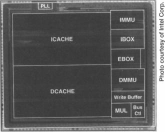
A photograph of a StrongARM die is shown in Figure 12.10 with an overlay indicat- |
SJlicon |
ing the major functional areas. The die area is, not surprisingly, dominated by the |
|
instruction cache (1CACHE) and the data cache (DCACHE). Each cache has its own |
|
MMU (IMMU and DMMU). The processor core has the instruction issue unit |
|
(IBOX) and the execution unit (EBOX) with high-speed multiplication hardware |
|
(MUL). The write buffer and external bus controller complete the processor logic. |
Figure 12.10 StrongARM die photograph.
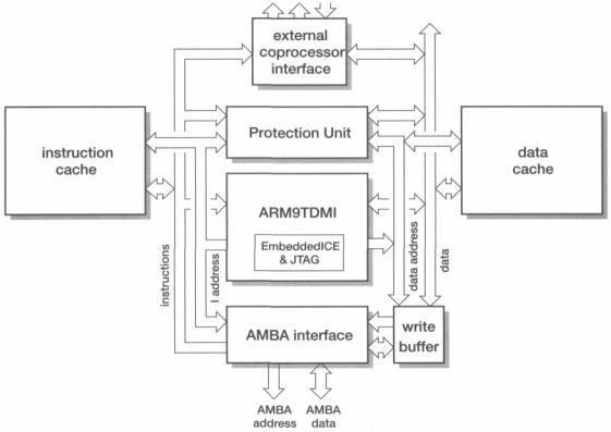
The ARM920T and ARM940T |
335 |
The high-frequency on-chip clock is generated by a phase-locked loop (PLL) from an external 3.68 MHz clock input.
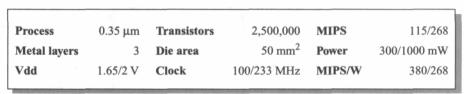
The characteristics of the StrongARM are summarized in Table 12.4.
Table 12.4 StrongARM characteristics.
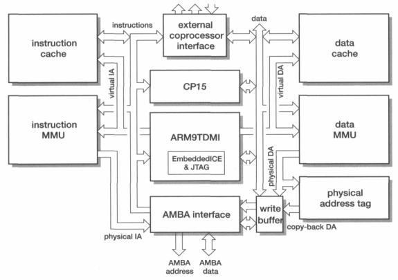
12.4The ARM920T and ARM940T
|
The ARM920T and ARM940T are based upon the ARM9TDMI processor core (see |
|
Section 9.3 on page 260), to which instruction and data caches have been added. |
|
The instruction and data ports are merged via an AMBA bus master unit, and a |
|
write buffer and memory management unit (ARM920T) or memory protection unit |
|
(ARM940T) are also incorporated. |
ARM920T |
The overall organization of the ARM920T is illustrated in Figure 12.11 on |
|
page 336. |
ARM920T |
The instruction and data caches are both 16 Kbytes in size and are built using a seg- |
caches |
mented CAM-RAM organization to give 64-way associativity. Each cache comprises |
|
eight segments of 64 lines, the required segment being addressed by A[7:5]. They |
|
have 8-word (32 byte) lines and support lock-down in units of 256 bytes (correspond- |
|
ing to one line in each segment). The replacement strategy is pseudo-random or |
|
round-robin, and is determined by the 'RR' bit (bit 14) in CP15 register 1. A complete |
|
8-word line is reloaded on a cache miss. |
|
The instruction cache is read-only. The data cache supports a copy-back write strat- |
|
egy, and each line has one valid bit, two dirty bits and a write-back bit. The write-back |
|
bit duplicates information usually found in the translation system, and enables the |
|
cache to implement a write operation as write-through or copy-back without reference |
|
to the MMU. When a cache line is replaced any dirty data is sent to the write buffer, |
|
and this may amount to zero, four or eight words depending on the two dirty bits. The |
|
data cache allocates space only on a read miss, not on a write miss. |
|
As the data cache is accessed using virtual addresses, there is a problem whenever |
|
dirty data has to be written back to main memory since this action requires the physical |
|
address. The ARMS 10 solves this by passing the virtual address back to the MMU |
338 |
ARM CPU Cores |
Figure 12.12 ARM940T organization.
The caches supports lock-down, which means that sections of the cache can be loaded and then the contents protected from being flushed. Locked-down sections of the cache are clearly unavailable for further general-purpose cache use, but the ability to guarantee that certain critical code sections will always be found in the cache may be more important than getting the best cache hit rate. The caches may be locked down in 16-word units.
The ARM9TDMI instruction port is used to load instructions and therefore only performs read operations. The only coherency problem arises when the program that the cache holds copies of is modified in main memory. Any modification of code (such as loading a new program into memory previously occupied by a program that is no longer required) must be handled carefully, and the instruction cache selectively or completely flushed before the new program is executed.
The ARM9TDMI data port supports writes as well as reads, and therefore the data cache must implement some sort of write strategy (see 'Write strategies' on page 278).