

Furber S.ARM system-on-chip architecture.2000
.pdfExamples and exercises |
289 |
10.6Examples and exercises
Example 10.1 |
How big can a 4-way physical cache be in a system with |
|
1 Kbyte pages? |
|
Assume we want to perform the TLB and cache accesses in parallel as described in |
|
'Virtual and physical caches' on page 287. |
|
Each section of the cache can be at most 1 Kbyte, so the maximum total cache size |
|
is 4 Kbytes. |
Exercise 10.1.1 |
How much memory does the tag store require in this cache if the line size is |
|
16 bytes? |
Exercise 10.1.2 |
Estimate the proportions of the areas of the TLB and the data cache tag and data |
|
memories in the above example. |
Example 10.2 |
How big would a TLB have to be to contain the translations for all of |
|
the physical pages? |
|
With 4 Kbyte pages, a 1 Mbyte memory contains 256 pages so the TLB needs 256 |
|
entries. The TLB need no longer be an automatic cache. Since a TLB miss means |
|
that the page is absent from physical memory a disk transfer is required, and the |
|
overhead of maintaining the TLB by software is negligible compared with the cost |
|
of the disk transfer. |
|
A TLB which covers all physical memory is a form of inverted page table, and |
|
just such a translation scheme was used on the early ARM memory controller chips |
|
used in the Acorn Archimedes machines. Referring to Figure 10.12 on page 288, the |
|
translation hardware can be a CAM; the physical page number store is a simple hard- |
|
wired encoder, and the CAM has one entry for each physical page. |
|
The Acorn memory controller chips had CAMs with 128 entries and a page size |
|
that varied according to the amount of physical memory in the system. A 1 Mbyte |
|
system had 8 Kbyte pages, a 4 Mbyte system had 32 Kbyte pages. To extend beyond |
|
4 Mbytes, the page size stayed at 32 Kbytes and a second memory controller was |
|
added. The CAMs were maintained by software, so no complex table-walking hard- |
|
ware was required. The full translation tables were entirely defined by software. |
Exercise 10.2.1 |
Estimate the die area of a 128-entry inverted page table compared with a 64 entry |
|
TLB, assuming that one bit of CAM requires twice the area of one bit of RAM. |

Architectural Support for Operating Systems
Summary of chapter contents
The role of an operating system is to provide an environment where several programs may run concurrently with a minimal risk of unwanted interference between them but with support for safe data sharing. The operating system should also provide a clean interface to the hardware facilities of the machine.
Interference between processes is minimized by memory management and protection schemes which enable each process to access only its own area of memory. The process is given its own view of the system memory, and when a process switch takes place the memory view is dynamically transformed to that of the new process, with all the memory used by the previous process being removed from sight. This requires sophisticated hardware support if it is to operate efficiently.
Data sharing implies a loophole in the protection scheme which must be controlled with great care. Haphazard access to shared structures can lead to the most obscure forms of program misbehaviour, so a disciplined approach must be applied.
Access to hardware facilities often involves a lot of low-level bit manipulation, and rather than require each process to do this independently, the details are usually handled centrally by the operating system. Processes can then access input/ output functions at a higher level through system calls.
The ARM architecture incorporates features specifically to support all these aspects of the operating system.
290
An introduction to operating systems |
291 |
11.1An introduction to operating systems
Multi-user systems
Memory
v
management
Protection
The role of an operating system is to present a uniform and clean interface between the underlying hardware resources of the machine and the application programs that run on it. The most sophisticated operating systems are those that provide facilities for multiple general-purpose programs run by several different users at the same time.
It is very inconvenient if a multi-user system requires each program to make allowances for the presence of other programs in the same machine, since the number and type of concurrent programs is unknown and will vary from one run to the next. Therefore a multi-user operating system presents each program with a complete virtual machine in which to operate. Each program can be written as though it is the only program running at the time; the only noticeable effect of the presence of other programs is that the program typically takes longer to run.
Although several programs may be present in the machine at one time, the processor has only one set of registers (we are not concerned with multi-processor systems here), so only one program is executing at any particular time. The apparent concurrency is achieved by time-slicing, which means that each program takes a turn in the processor. Since the processor operates at very high speeds by human standards, the effect is that over a period of, say, a second each program will have had several goes in the processor so all programs make some progress. The operating system is responsible for scheduling (deciding which program runs when), and it may give each program an equal share of the CPU time or it may use priority information to favour some programs over others.
A program is switched out of the processor either because the operating system is invoked by a timer interrupt and decides the program has had enough time for now, or because the program has requested a slow peripheral access (such as a disk access) and cannot do any more useful work until it gets a response. Rather than leave the program idling in the processor, the operating system switches it out and schedules another program that can make useful progress.
In order to create the virtual machine in which a program runs, the operating system must establish an environment where the program has access to its code and data at the memory locations where it expects to find them. Since one program's expectations of the addresses it will use may conflict with another's, the operating system uses memory translation to present the physical memory locations where it has loaded the code and data to the program at appropriate logical addresses. The program sees the memory through a logical-to-physical address translation mechanism which is managed by the operating system.
Where several users are running programs on the same machine it is highly desirable to ensure that an error in one user's program cannot interfere with the operation of any of the other programs. It is also, unfortunately, necessary to protect against malicious attempts to interfere with other programs.
292
Resource allocation
Single-user systems
Architectural Support for Operating Systems
The memory-mapping hardware which gives each program its own virtual machine can also ensure that a program cannot see any memory belonging to another program, thereby providing a measure of protection. It is not efficient to enforce this too far, however, since sharing areas of memory that contain, for example, libraries of useful functions can save on memory use. A solution here is to make these areas read-only or execute-only so one program cannot corrupt code that will be used by another.
An obvious route for a malicious user to cause damage to another is to overcome the protection afforded by the memory-management system by assuming operating system status and then changing the translation tables. Most systems address this by providing a privileged system mode which has controlled access and making the translation tables accessible only from this mode.
Designing a computer system to be secure against malicious attacks by clever individuals is a complex issue which requires some architectural support. On the ARM this support is provided by privileged processor modes with controlled access and various forms of memory protection in the memory management units. However, few ARMs are used in systems where protection against malicious users is required, so most of the time these facilities are used to catch inadvertent programming errors and thereby help debug the software.
Two programs which are running concurrently may place conflicting demands on system resources. For example, one program may request data from one part of a disk. It will be switched out while the disk drive seeks the data, and the program that gets switched in may immediately request data from a different part of the disk. If the disk drive responds directly to these requests a situation can easily arise where the programs alternately have control and the disk drive oscillates between the two seeks, never having long enough to find either data area, and the system will live-lock until the disk drive wears out.
In order to avoid this sort of scenario, all requests for input/output activity are channelled through the operating system. It will accept the request from the first program and then queue up the request from the second program to receive attention once the first has been satisfied.
Where a system serves a single user, still possibly running several programs at the same time, much of the above continues to apply. Although the threat of a malicious user sharing the same machine is removed, it is still very useful for each program to run in its own space so that an error in one program does not cause errors in another. The simplification that arises from removing the concern about the malicious user is that it is no longer necessary to make it impossible for a program to assume system privileges, it should merely be extremely unlikely that this will happen inadvertently.
However, desktop machines that appear to belong to one user are increasingly being connected to computer networks that allow other users to run programs on them
The ARM system control coprocessor |
293 |
Embedded systems
Chapter structure
remotely. Such machines should clearly be viewed as multi-user and incorporate appropriate levels of protection.
An embedded system is quite different from the singleand multi-user general-purpose system discussed above. It typically runs a fixed set of programs and has no mechanism for introducing new programs. Presumably, then, the problem of the malicious user has been removed.
The operating system continues to play a similar role, giving each active program a clean virtual machine in which to run, providing protection for one program from errors in another and scheduling the use of CPU time.
Many embedded systems operate within real-time constraints which must be allowed to determine scheduling priorities. Cost issues also preclude the use of the operating systems that are popular on general-purpose machines, since these tend to demand large memory resources. This has led to the development of the real-time operating system (RTOS) which provides the scheduling and hardware interface facilities required by an embedded system using just a few kilobytes of memory.
Smaller embedded systems may not even be able to bear this cost, or they may have such simple scheduling requirements (for example, one fixed program that runs all the time) that they do not need an 'operating system' at all. Here a simple 'monitor' program suffices, providing a few system functions such as sanitized interfaces to input/ output functions. Such systems almost certainly dispense with the memory management hardware and use the processor's logical address to access memory directly. If an embedded system includes a cache memory some mechanism is required to define which areas of memory are cacheable (since I/O areas should not be cached), but this can be far simpler than a full memory management system.
The general principles of memory management were described in the previous chapter. Subsequent sections in this chapter introduce the ARM system control coprocessor and the memory management systems it controls, which include a full MMU with address translation and a simpler 'protection unit' for embedded systems that do not require address translation.
Following this there are sections on the important operating system related issues of synchronization, context switching and the handling of input/output devices, including the use of interrupts.
11.2The ARM system control coprocessor
The ARM system control coprocessor is an on-chip coprocessor, using logical coprocessor number 15, which controls the operation of the on-chip cache or caches, memory management or protection unit, write buffer, prefetch buffer, branch target cache and system configuration signals.

294 Architectural Support for Operating Systems
CP15 |
The control is effected through the reading and writing of the CP15 registers. The |
instructions |
registers are all 32 bits long, and access is restricted to MRC and MCR instructions |
|
(see Section 5.19 on page 139) which must be executed in supervisor mode. Use of |
|
other coprocessor instructions or any attempted access in user mode will cause the |
|
undefined instruction trap to be taken. The format of these instructions is shown in |
|
Figure 11.1. In most cases the CRm and Cop2 fields are unused and should be zero, |
|
though they are used in certain operations. |
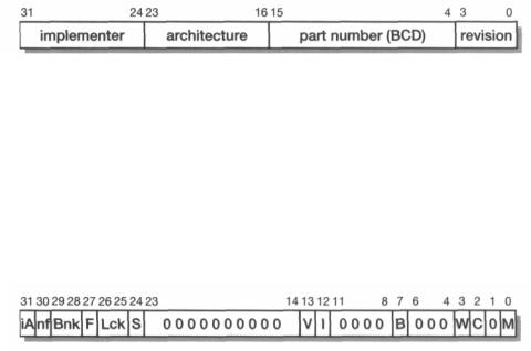
Figure 11.1 CP15 register transfer instructions.
Protection unit ARM CPUs which are used in embedded systems with fixed or controlled application programs do not require a full memory management unit with address translation capabilities. For such systems a simpler protection unit is adequate. The CP15 register organization for the ARM protection units is described in Section 11.3, and the operation of the protection unit is described in Section 11.4 on page 297.
The CPUs which use a protection unit are the ARM740T described in Section 12.1 on page 318 and the ARM940T described in Section 12.4 on page 335.
MMU |
ARM CPUs for use in general-purpose applications where the range and number of |
|
application programs is unknown at design time will usually require a full memory |
|
management unit with address translation. The CP15 register organization for the |
|
ARM MMU is described in Section 11.5 on page 298 and the operation of the |
|
MMU is described in Section 11.6 on page 302. |
|
CPUs which use the full MMU include all the other CPUs described in Chapter 12. |
11.3 CP15 protection unit registers
The protection unit register structure is illustrated in Table 11.1 on page 295. The registers are read and written using the CP15 instruction shown in Figure 11.1, with CRn specifying the register to be accessed. In detail, the register functions are as follows:
CP15 protection unit registers |
295 |
||
|
Table 11.1 |
CP15 protection unit register structure. |
|
|
|
|
|
Register |
Purpose |
|
|
|
|
|
|
0 |
ID Register |
|
|
1 |
Configuration |
|
|
2 |
Cache Control |
|
|
3 |
Write Buffer Control |
|
|
5 |
Access Permissions |
|
|
6 |
Region Base and Size |
|
|
7 |
Cache Operations |
|
|
9 |
Cache Lock Down |
|
|
15 |
Test |
|
|
4,8,10-14 |
UNUSED |
|
|
|
|
|
|
Register 0 (which is read-only) returns device identification information.
Bits [3:0] contain a revision number, bits [15:4] contain a 3-digit part number in binary-coded decimal, bits [23:16] contain the architecture version (0 for version 3, 1 for version 4, 2 for version 4T, 4 for version 5T) and bits [31:24] contain the ASCII code of an implementer's trademark (ASCII 'A' = 4116 indicates ARM Limited, 'D' = 44I6 indicates Digital, and so on).
Some CPUs do not follow the above register 0 format exactly, and recent CPUs have a second register 0 (accessed by changing the Cop2 field in the MRC instruction) which gives details on the cache organization.
Register 1 (which is read-write) contains several bits of control information which enable system functions and control system parameters.
All bits are cleared on reset. If subsequently set, M enables the protection unit, C enables the data or unified cache, W enables the write buffer, B switches from little- to big-endian byte ordering, I enables the instruction cache when this is separate from the data cache, V causes the exception vectors to move to near the top
296 |
Architectural Support for Operating Systems |
of the address space, S, Lck, F and Bnk are used to control the cache (on the ARM740T), and nf and iA control various clock mechanisms (on the ARM940T).
Note that not all bits are provided in all implementations.
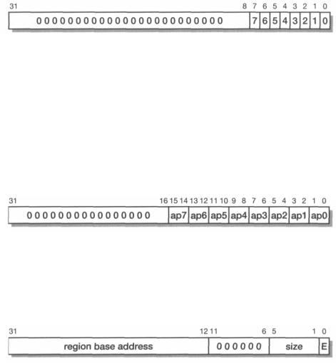
• Register 2 (which is read-write) controls the cacheability of the eight individual protection regions.
Bit 0 enables the cache for loads within region 0, bit 1 likewise for region 1, and so on. The ARM940T has separate protection units on its instruction and data ports, and Cop2 (see Figure 11.1 on page 294) is used to determine which unit is accessed: Cop2 = 0 gives access to the protection unit on the data port; Cop2 = 1 gives access to the protection unit on the instruction port.
•Register 3 (which is read-write) defines whether or not the write buffer should be used for each of the protection regions. Its format is the same as that for register 2, but note that as the ARM940T instruction port is read-only, the write buffer can only be enabled for the data port and so Cop2 should always be zero.
•Register 5 (which is read-write) defines the access permissions for each of the protection regions.
The access permissions cover no access (00), privileged modes only (01), privileged full access and user read only (10) and full access (11). Again the ARM940T uses the Cop2 field to differentiate the instruction (1) and data (0) protection units.
•Register 6 (which is read-write) defines the start address and size of each of the eight regions.
The region base address must be a multiple of the size. The encoding of the size field is shown in Table 11.2 on page 298. E enables the region.
The particular region is specified in the CRm field (see Figure 11.1 on page 294) which should be set from 0 to 7. For a Harvard core such as the ARM940T there
ARM protection unit |
297 |
are separate region registers for the instruction and data memory ports, and Cop2 specifies which memory port is to be addressed as described above for register 2.
Register 7 controls various cache operations and its operation is different for the ARM740T and the ARM940T.
Register 9 is used in the ARM940T to lock down areas of the cache. (The ARM740T uses certain bits in register 1 for this purpose.)
Register 15 is used in the ARM940T to modify the cache allocation algorithm from random to round-robin. This is intended for use only during silicon production testing.
11.4ARM protection unit
|
ARM CPUs intended for embedded applications incorporate a memory protection |
|
unit which defines various protection and cache functions for different regions of |
|
memory so that, for example, I/O regions can be restricted to supervisor access only |
|
and made uncacheable. Protection units do not translate addresses. Systems which |
|
require address translation should use a full memory management unit, described in |
|
Section 11.6 on page 302. CPUs which incorporate the protection unit include the |
|
ARM740T and the ARM940T. |
Protection unit |
The protection unit allows the ARM 4 Gbyte address space to be mapped into eight |
structure |
regions, each with a programmable start address and size and with programmable protec- |
|
tion and cache properties. The regions may overlap. A fixed priority scheme defines those |
|
characteristics which apply to an address which falls into more than one region. |
Region definition |
Each of the eight regions has a start address and a size defined by writing to CP15 |
|
register 6. The format of this register was defined on page 296. The minimum region |
|
size is 4 Kbytes, the maximum 4 Gbytes. Rd[5:l], when written to CP15 register 6, |
|
defines the size, which can be set to any power of two bytes between the maximum |
|
and minimum as shown in Table 11.2 on page 298. The start address must be a mul- |
|
tiple of the selected size and is defined by Rd[31:12]. The region will have no effect |
|
unless it is enabled by setting Rd[0]. |
Region priorities |
The regions may legitimately be programmed so that they overlap. When an address |
|
that falls into more than one region is presented to the protection unit a fixed prior- |
|
ity scheme determines which region defines its attributes: region 7 has the highest |
|
priority, region 0 the lowest, and the other regions have intermediate priorities in |
|
order of their number. |
298 Architectural Support for Operating Systems
|
|
Table 11.2 |
Protection unit region size encoding. |
|
|
|
|
|
|
Rd[5:l] |
Region size |
|
|
|
|
|
|
|
|
01011 |
4 Kbytes |
|
|
|
01100 |
8 Kbytes |
|
|
|
01101 |
16 Kbytes |
|
|
|
01110 |
32 Kbytes |
|
|
|
11100 |
5 12 Mbytes |
|
|
|
11101 |
1 Gbyte |
|
|
|
11110 |
2 Gbytes |
|
|
|
11111 |
4 Gbytes |
|
|
|
|
|
|
the start of a region, which must be a multiple of its size, means |
|
|
|
The restriction on |
||
|
|
that checking whether or not an address falls within a region is simply a matter of |
||
|
|
comparing some number (up to 20) of the most significant bits of the address against |
||
|
|
the corresponding bits of the region start address. If they match, the address falls |
||
|
|
inside that region. If they don't match, the address falls outside the region. No addition |
||
|
|
or subtraction is required, so the process can be fast. The organization of the protec- |
||
|
|
tion unit is therefore as shown in Figure 11.2 on page 299. In this illustration region 0 |
||
|
|
cover the complete 4 Gbyte address space and therefore all addresses fall into it. |
||
|
|
Regions 1, 2 and 4 are 4 Kbytes, and regions 3, 6, 7 and 5 have increasing sizes. The |
||
|
|
example address falls in regions 0, 3 and 6 (as denoted by the black arrows), so the |
||
|
|
priority encoder selects the attributes for the highest priority region, region 6. |
||
|
|
If an address does not fall into any enabled region the protection unit will generate |
||
|
|
an abort. |
|
|
Harvard cores |
ARM cores that use a Harvard architecture (such as the ARM940T) have separate pro- |
|||
|
|
tection units on their instruction and data ports, so they have a total of 16 regions. |
||
11.5CP15 MMU registers
The MMU register structure is illustrated in Table 11.3 on page 299. The registers are read and written using the CP15 instruction shown in Figure 11.1 on page 294, with CRn specifying the register to be accessed.
In detail, the register functions are as shown on page 300.