


Functional Overview
2.3PrimeCell SSPMS operation
The operation of the PrimeCell SSPMS is described in the following sections:
•Interface reset
•Configuring the SPP PL021
•Enable PrimeCell SSP operation on page 2-8
•Clock signals on page 2-8
•Programming the SSPCR0 Control Register on page 2-8
•Programming the SSPCR1 Control Register on page 2-9
•Frame format on page 2-10
•Texas Instruments synchronous serial frame format on page 2-11
•Motorola SPI frame format on page 2-12
•National Semiconductor Microwire frame format on page 2-17
•Examples of master and slave configurations on page 2-19.
2.3.1Interface reset
The PrimeCell SSPMS is reset by the global reset signal BnRES and a block-specific reset signal nSSPRST. An external reset controller must use BnRES to assert nSSPRST asynchronously and negate it synchronously to SSPCLK. BnRES should be asserted LOW for a period long enough to reset the slowest block in the on-chip system, and then taken HIGH again. The PrimeCell SSPMS requires BnRES to be asserted LOW for at least one period of PCLK.
The values of the registers after reset are described in Chapter 3 Programmer’s Model.
2.3.2Configuring the SPP PL021
Following reset, the PrimeCell SSPMS logic is disabled and should be configured in this state.
Control registers SSPCR0 and SSPCR1 need to be programmed to configure the peripheral as a master or slave operating under one of the following protocols:
•Motorola SPI
•Texas Instruments SSI
•National Semiconductor.
The bit rate, derived from the external SSPCLK, requires the programming of the clock pre-scale register SSPCPSR.
ARM DDI 0171B |
Copyright © ARM Limited 1999. All rights reserved. |
2-7 |

Functional Overview
2.3.3Enable PrimeCell SSP operation
You can either prime the transmit FIFO, by writing up to eight 16-bit values when the SSPMS is disabled, or allow the transmit FIFO service request to interrupt the CPU. Once enabled, transmission or reception of data begins on the transmit (SSPTXD) and receive (SSPRXD) pins.
2.3.4Clock signals
The frequency selected for SSPCLK must accommodate the desired range of bit clock rates:
FSSPCLK(min) >=2 * FSCLKOUT(max)
FSSPCLK(max) <=254 * 256 * FSCLKOUT(min)
For example, for a range of bit clocks from 7.2kHz to 1.8432MHz the SSPCLK frequency must be within the range 3.6864MHz to 468MHz.
The frequency of SSPCLK must be chosen to be within the required error limits for all baud rates to be used.
There is also constraint on the ratio of clock frequencies for PCLK to SSPCLK. The frequency of SSPCLK must be less than or equal to the frequency of PCLK.
FSSPCLK <= FPCLK
2.3.5Programming the SSPCR0 Control Register
Refer to Chapter 3 Programmer’s Model for more details on the bit assignment of this register.
The SSPCR0 register is used to:
•program the serial clock rate
•select one of the three protocols
•select the data word size (where applicable).
The serial clock rate value (SCR), in conjunction with the SSPCPSR clock pre-scale divisor value (CPSDVSR), is used to derive the SSPMS transmit and receive bit rate from the external SSPCLK.
The frame format is programmed via the FRF bits and the data word size via the DSS bits.
Bit phase and polarity, applicable to Motorola SPI format only, are programmed via the SPH and SPO bits.
2-8 |
Copyright © ARM Limited 1999. All rights reserved. |
ARM DDI 0171B |

Functional Overview
2.3.6Programming the SSPCR1 Control Register
Refer to Chapter 3 Programmer’s Model, for more details on the bit assignment of this register.
The SSPCR1 register is used to:
•select master or slave mode
•control interrupt enabling or disabling
•enable a loop back test feature
•enable the SSPMS peripheral.
To configure the SSPMS as a master, clear the SSPCR1 register master or slave selection bit (MS) to 0, which is the default value on reset.
Setting the SSPCR1 register MS bit to 1 configures the SSPMS as a slave. When configured as a slave, enabling or disabling of the SSPMS SSPTXD signal is provided through the SSPCR1 slave mode SSPTXD output disable bit (SOD). This can be used in some multi-slave environments where masters may parallel broadcast.
You can enable the transmit and receive FIFO level interrupts by setting the respective
Transmit Interrupt Enable (TIE), Receive Interrupt Enable (RIE) and Receive FIFO OverRun Interrupt Enable (RORIE) bits within the SSPCR1 register.
To enable the operation of the SSPMS set the Synchronous Serial Port Enable (SSE) bit to 1.
Bit rate generation
The serial bit rate is derived by dividing down the input clock SSPCLK. The clock is first divided by an even prescale value CPSDVSR from 2 to 254, which is programmed in SSPCPSR. The clock is further divided by a value from 1 to 256, which is 1 + SCR, where SCR is the value programmed in SSPCR0.
The frequency of the output signal bit clock SCLKOUT is defined below:
FSSPCLK
F = ---------------------------------------------------------
SC LKO UT CPSDVR × (1 + SCR)
For example, if SSPCLK is 3.6864 MHz, and CPSDVSR = 2, then SCLKOUT has a frequency range from 7.2 kHz to 1.8432 MHz.
ARM DDI 0171B |
Copyright © ARM Limited 1999. All rights reserved. |
2-9 |

Functional Overview
2.3.7Frame format
Each data frame is between 4 and 16 bits long depending on the size of data programmed, and is transmitted starting with the MSB. There are three basic frame types that can be selected:
•Texas Instruments synchronous serial
•Motorola SPI
•National Semiconductor Microwire.
For all three formats the serial clock (SCLKOUT) is held LOW or inactive while the PrimeCell SSPMS is idle, and transitions at the programmed frequency only during active transmission of data.
For Motorola SPI and National Semiconductor Microwire frame formats, the serial frame (SFRMOUT) pin is active LOW, and is asserted (pulled down) during the entire transmission of the frame. The type of serial clock edges used to drive and sample data are also the same for these two formats. Both the PrimeCell SSPMS and the off-chip slave device drive their output data on the falling edge of SCLKOUT, and latch data from the other device on the rising edge.
For Texas Instruments synchronous serial frame format, the SFRMOUT pin is pulsed for one serial clock period starting at its rising edge, prior to the transmission of each frame. For this frame format, both the PrimeCell SSPMS and the off-chip slave device drive their output data on the rising edge of SCLKOUT, and latch data from the other device on the falling edge.
Unlike the full-duplex transmission of the other two frame formats, the National Semiconductor Microwire format uses a special master-slave messaging technique, which operates at half-duplex. In this mode, when a frame begins, an 8-bit control message is transmitted to the off-chip slave. During this transmit, no incoming data are received by the SSPMS. After the message has been sent, the off-chip slave decodes it and, after waiting one serial clock after the last bit of the 8-bit control message has been sent, responds with the requested data. The returned data can be 4 to 16 bits in length, making the total frame length anywhere from 13 to 25 bits.
2-10 |
Copyright © ARM Limited 1999. All rights reserved. |
ARM DDI 0171B |
Functional Overview
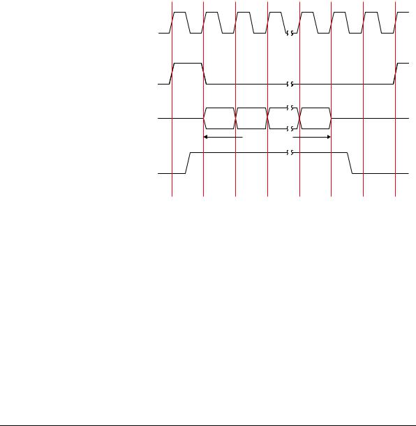
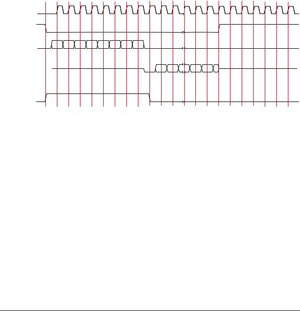
2.3.8Texas Instruments synchronous serial frame format
Figure 2-2 shows the Texas Instruments synchronous serial frame format for a single transmitted frame.
|
Single transfer |
|
|
SCLKOUT/ |
|
|
|
SCLKIN |
|
|
|
SFRMOUT/ |
|
|
|
SFRMIN |
|
|
|
SSPTXD/ |
MSB |
LSB |
|
SSPRXD |
|||
|
|
||
|
4 to 16 bits |
|
|
SSPOE |
|
|
Figure 2-2 Texas Instruments synchronous serial frame format (single transfer)
In this mode, SCLKOUT and SFRMOUT are forced LOW, and the transmit data line SSPTXD is tristated whenever the PrimeCell SSPMS is idle. Once the bottom entry of the transmit FIFO contains data, SFRMOUT is pulsed HIGH for one SCLKOUT period. The value to be transmitted is also transferred from the transmit FIFO to the serial shift register of the transmit logic. On the next rising edge of SCLKOUT, the MSB of the 4 to 16 bit data frame is shifted out on the SSPTXD pin. Likewise, the MSB of the received data is shifted onto the SSPRXD pin by the off-chip serial slave device.
Both the PrimeCell SSPMS and the off-chip serial slave device then clock each data bit into their serial shifter on the falling edge of each SCLKOUT. The received data are transferred from the serial shifter to the receive FIFO on the first rising edge of SCLKOUT after the LSB has been latched.
ARM DDI 0171B |
Copyright © ARM Limited 1999. All rights reserved. |
2-11 |
Functional Overview
SCLKOUT/
SCLKIN
SFRMOUT/
SFRMIN
SSPTXD/
SSPRXD
SSPOE (=1)
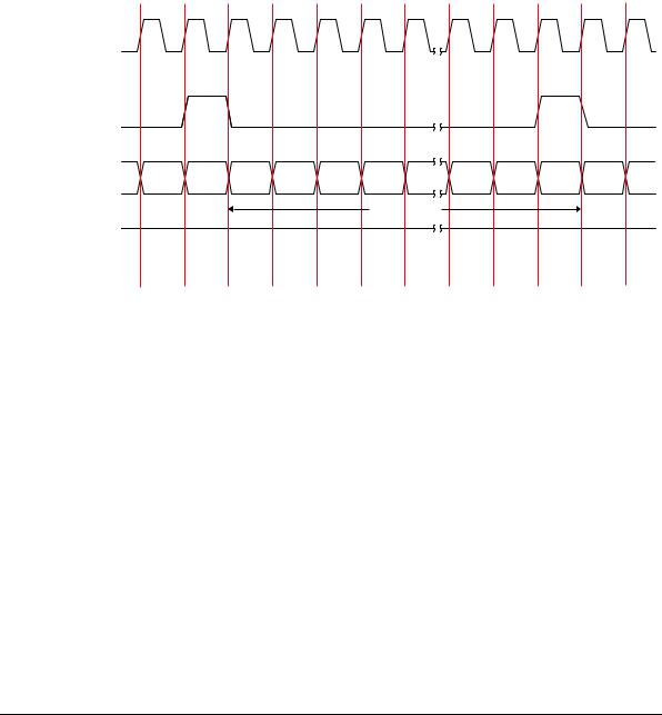
Figure 2-3 shows the Texas Instruments synchronous serial frame format when back to back frames are transmitted.
Continuous transfer
MSB |
LSB |
4 to 16 bits
Figure 2-3 TI synchronous serial frame format (continuous transfer)
2.3.9Motorola SPI frame format
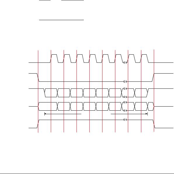
Figure 2-4 on page 2-13 shows the Motorola SPI frame format for a single frame. Figure 2-5 on page 2-14 shows the same format when back to back frames are transmitted.
In this mode, SCLKOUT is forced LOW, SFRMOUT is forced HIGH, and the transmit data line (SSPTXD) is tristated whenever the PrimeCell SSPMS is idle. Once the bottom entry of the transmit FIFO contains data, SFRMOUT is pulled LOW and remains LOW for the duration of the frame transmission. The falling edge of SFRMOUT causes the value for transmission to be transferred from the bottom transmit FIFO entry to the serial shift register of the transmit logic. The MSB of the 4 to 16 bit data frame is then shifted out onto the SSPTXD pin half an SCLKOUT period later. The SCLKOUT pin does not transition at this point.
2-12 |
Copyright © ARM Limited 1999. All rights reserved. |
ARM DDI 0171B |
SCLKOUT/ SCLKIN
SFRMOUT/ SFRMIN
SSPTXD
SSPRXD
SSPOE
Functional Overview
The MSB of the received data is shifted onto the SSPRXD pin by the off-chip slave device as soon as the serial framing signal goes LOW. Both the PrimeCell SSPMS and the off-chip serial slave device then latch each data bit into their serial shifter on the rising edge of each SCLKOUT. At the end of the frame, the SFRMOUT pin is pulled HIGH one SCLKOUT period after the last bit has been latched in the receive serial shifter. This causes the data to be transferred to the receive FIFO.
Note
The off-chip slave device can tristate the receive line either on the falling edge of SCLKOUT after the LSB has been latched by the receive shifter, or when the SFRMOUT pin goes HIGH.
Single transfer
SPH = 0, SPO = 0
MSB |
LSB |
MSB |
LSB Q |
|
4 to 16 bits |
Figure 2-4 Motorola SPI frame format (single transfer)
ARM DDI 0171B |
Copyright © ARM Limited 1999. All rights reserved. |
2-13 |

Functional Overview
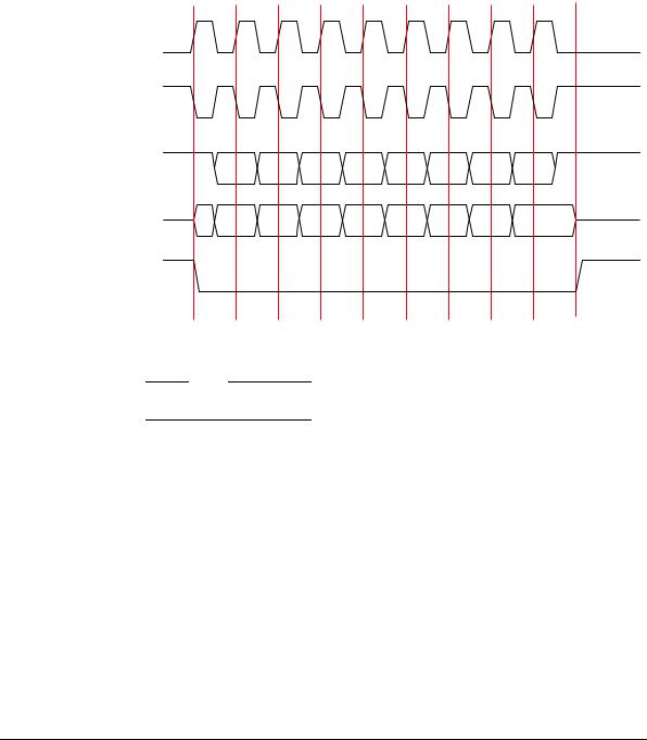
Figure 2-5 shows the Motorola SPI frame format when back to back frames are transmitted.
Continuous transfer
SPH = 0, SPO = 0
SCLKOUT/
SCLKIN
SFRMOUT(=0)/
SFRMIN(=0)
SSPTXD/ |
MSB |
LSB |
|
SSPRXD |
|||
|
|
||
|
|
4 to 16 bits |
|
SSPOE (=1) |
|
|
Figure 2-5 Motorola SPI frame format (continuous transfer)
It is possible to change the Motorola clock phase and polarity by selecting the appropriate value of SPO and SPH in the control register SSPCR0.
2-14 |
Copyright © ARM Limited 1999. All rights reserved. |
ARM DDI 0171B |
Functional Overview
The operation of SPO and SPH is shown in Figure 2-6, and Figure 2-7 on page 2-16.
SCLKOUT/
SCLKIN (SPO = 0)
SCLKOUT/
SCLKIN (SPO = 1)
SSPTXD |
MSB |
LSB |
|
from master |
|||
|
|
||
SSPRXD |
MSB |
LSB Q |
|
from slave |
|||
|
|
||
SFRMOUT/ |
|
|
|
SFRMIN |
|
|
|
|
|
Figure 2-6 Motorola SPI frame format with SPH = 0 |
Note
In Figure 2-6 Q is an undefined signal.
ARM DDI 0171B |
Copyright © ARM Limited 1999. All rights reserved. |
2-15 |
Functional Overview
SCLKOUT/
SCLKIN (SP0 = 0)
SCLKOUT/
SCLKIN (SP0 = 1)
SSPTXD |
MSB |
LSB |
|
from master |
|||
|
|
||
SSPRXD |
Q MSB |
LSB |
|
|
|||
from slave |
|
|
|
SFRMOUT/ |
|
|
|
SFRMIN |
|
|
|
|
|
Figure 2-7 Motorola SPI frame format with SPH = 1 |
Note
In Figure 2-7 Q is an undefined signal.
For continuous transfers (see Figure 2-5 on page 2-14) data transmission begins and ends in the same manner as a single transfer. However, the SFRMOUT line is continuously asserted (held LOW). The transmission of data also occurs back to back (the MSB of the next frame follows directly after the LSB of the current frame). Each of the received data values is transferred from the receive shifter to the receive FIFO on the falling edge of SCLKOUT, after the LSB of the frame has been latched into the PrimeCell SSPMS.
2-16 |
Copyright © ARM Limited 1999. All rights reserved. |
ARM DDI 0171B |
Functional Overview
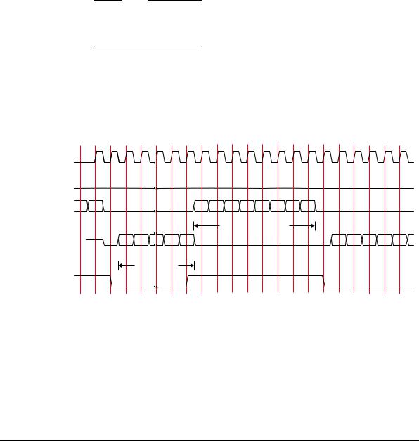
2.3.10National Semiconductor Microwire frame format
Figure 2-8 shows the National Semiconductor Microwire frame format, again for a single frame. Figure 2-9 on page 2-18 shows the same format when back to back frames are transmitted.
SCLKOUT/
SCLKIN
SFRMOUT/
SFRMIN
SSPTXD
MSB |
8-bit control |
LSB |
SSPRXD |
|
0 |
MSB 4 to 16 bits LSB  output data

SSPOE
Figure 2-8 Microwire frame format, single transfer
Microwire format is very similar to SPI format, except that transmission is half-duplex instead of full-duplex, using a master-slave message passing technique. Each serial transmission begins with an 8-bit control word that is transmitted from the PrimeCell SSPMS to the off-chip slave device. During this transmission, no incoming data are received by the PrimeCell SSPMS. After the message has been sent, the off-chip slave decodes it and, after waiting one serial clock after the last bit of the 8-bit control message has been sent, responds with the required data. The returned data is 4 to 16 bits in length, making the total frame length anywhere from 13 to 25 bits.
Like SPI mode, SCLKOUT is forced LOW, SFRMOUT is forced HIGH, and the transmit data line SSPTXD is tristated whenever the PrimeCell SSPMS is idle. A transmission is triggered by writing a control byte to the transmit FIFO. The falling edge of SFRMOUT causes the value contained in the bottom entry of the transmit FIFO to be transferred to the serial shift register of the transmit logic, and the MSB of the 8-bit control frame to be shifted out onto the SSPTXD pin. SFRMOUT remains LOW for the duration of the frame transmission. The SSPRXD pin remains tristated during this transmission.
The off-chip serial slave device latches each control bit into its serial shifter on the rising edge of each SCLKOUT. After the last bit is latched by the slave device, the control byte is decoded during a one clock wait-state, and the slave responds by transmitting data back to the PrimeCell SSPMS. Each bit is driven onto SSPRXD line
ARM DDI 0171B |
Copyright © ARM Limited 1999. All rights reserved. |
2-17 |
Functional Overview
on the falling edge of SCLKOUT. The PrimeCell SSPMS in turn latches each bit on the rising edge of SCLKOUT. At the end of the frame, for single transfers, the SFRMOUT signal is pulled HIGH one clock period after the last bit has been latched in the receive serial shifter, which causes the data to be transferred to the receive FIFO.
Note
The off-chip slave device can tristate the receive line either on the falling edge of
SCLKOUT after the LSB has been latched by the receive shifter, or when the
SFRMOUT pin goes HIGH.
For continuous transfers, data transmission begins and ends in the same manner as a single transfer. However, the SFRMOUT line is continuously asserted (held LOW) and transmission of data occurs back to back. The control byte of the next frame follows directly after the LSB of the received data from the current frame. Each of the received values is transferred from the receive shifter on the falling edge SCLKOUT, after the LSB of the frame has been latched into the PrimeCell SSPMS.
SCLKOUT/
SCLKIN
SFRMOUT/
SFRMIN
SSPTXD
LSB |
MSB |
LSB |
|
8-bit control |
|
|
|
SSPRXD 0
MSB 4 to 16 bits LSB |
MSB |
output data |
|
SSPOE
Figure 2-9 Microwire frame format, continuous transfers
Setup and hold time requirements on SFRMIN with respect to SCLKIN in Microwire mode
In the Microwire mode, the PrimeCell SSP slave samples the first bit of receive data on the rising edge of SCLKIN after SFRMIN has gone LOW. Masters that drive a freerunning SCKLIN must ensure that the SFRMIN signal has sufficient setup and hold margins with respect to the rising edge of SCLKIN.
2-18 |
Copyright © ARM Limited 1999. All rights reserved. |
ARM DDI 0171B |

Functional Overview
Figure 2-10 illustrates these setup and hold time requirements. With respect to the SCLKIN rising edge on which the first bit of receive data is to be sampled by the PrimeCell SSP slave, SFRMIN should have a setup of at least two times the period of SSPCLK on which the PrimeCell SSP operates. With respect to the SCLKIN rising edge previous to this edge, SFRMIN should have a hold of at least one SSPCLK period.
t Hold = t SSPCLK |
t Setup = (2*t |
SSPCLK |
) |
||||||
|
|
|
|
|
|
|
|
|
|
|
|
|
|
|
|
|
|
|
|
SCLKIN
SFRMIN
SSPRXD
First RX data bit to be sampled by SSP slave
Figure 2-10 Microwire frame format, SFRMIN input setup and hold requirements
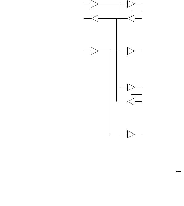
2.3.11Examples of master and slave configurations
The following diagrams show how the SSPMS PL021 Master and Slave peripheral could be connected to other synchronous serial peripherals, when the SPP PL021 is configured as a master or slave.
Note
The SSPMS PL021 does not support dynamic switching between master and slave in a system, each instance is configured and connected either as a master or slave.
ARM DDI 0171B |
Copyright © ARM Limited 1999. All rights reserved. |
2-19 |

Functional Overview
PL021 configured as master
SSPTXD |
|
SSPRXD |
|
||
SSPOE |
|
SSPOE |
SSPRXD |
|
SSPTXD |
SFRMOUT |
|
SFRMIN |
|
|
PL021 configured |
|
|
as slave |
SFRMIN |
|
SFRMOUT |
SCLKOUT |
|
SCLKIN |
SSPCTLOE |
|
SSPCTLOE |
SCLKIN |
|
SCLKOUT |
|
|
|
|
|
|
SSPRXD
SSPOE
SSPTXD
SFRMIN
PL021 configured as slave
SFRMOUT
SCLKIN
SSPCTLOE
SCLKOUT
Figure 2-11 SSPMS (PL021) master coupled to two slaves
Figure 2-11 shows the SSPMS PL021 instanced three times, as a single master and two slaves. It is possible for the master to broadcast to the two slaves via the master SSPTXD line. In response, only one slave will drive its SSPOE signal high, thereby enabling its SSPTXD data onto the masters SSPRXD line.
2-20 |
Copyright © ARM Limited 1999. All rights reserved. |
ARM DDI 0171B |

Functional Overview
|
|
|
|
|
|
|
|
SSPTXD |
|
|
|
|
|
MOSI |
|
SSPOE |
|
|
|
|
|
|
|
SSPRXD |
|
|
|
|
|
MISO |
|
SFRMOUT |
|
|
|
|
|
|
|
PL021 Configured |
|
|
|
|
|
|
SPI Slave |
As Master |
|
|
|
|
|
|
|
SFRMIN |
|
|
|
|
|
|
|
SCLKOUT |
|
|
|
|
|
SCK |
|
SSPCTLOE |
|
|
|
|
|
|
|
|
|
|
|
|
|
SS |
|
SCLKIN |
|
|
|
|
|
|
|
|
|
0V |
|
|
|
||
|
|
|
|
|
|
|
|
|
|
|
|
|
|
|
|
MOSI
MISO
SPI Slave
SCK
SS
0V
Figure 2-12 SSPMS (PL021) master coupled to two SPI slaves
Figure 2-12 shows how an SSPMS PL021, configured as master, would interface to two Motorola SPI slaves. Each SPI Slave Select (SS) signal is permanently tied LOW and configures them as slaves. Similar to the above operation, it is possible for the master to broadcast to the two slaves via the master SSPMS SSPTXD line. In response, only one slave will drive its SPI MISO port onto the master’s SSPRXD line.
ARM DDI 0171B |
Copyright © ARM Limited 1999. All rights reserved. |
2-21 |
Functional Overview
|
|
|
|
|
|
|
|
|
|
|
|
MOSI |
|
|
|
|
|
|
|
SSPRXD |
|||
|
|
|
|
|
|
|
|
|
|
|
SSPOE |
MISO |
|
|
|
|
|
|
|
SSPTXD |
|||
|
|
|
|
|
|
|
|
|
|
|
SFRMIN |
SPI Master |
|
|
|
|
|
|
|
PL021 Configured |
|||
|
|
|
|
|
|
|
|||||
|
|
|
|
0V |
As Slave |
||||||
|
|
|
|
|
|
|
|
||||
|
|
|
|
|
|
|
|
|
|
|
SFRMOUT |
SCK |
|
|
|
|
|
|
|
SCLKIN |
|||
|
|
|
|
|
|
|
|
|
|
|
SSPCTLOE |
|
|
|
|
|
Vdd |
|
|||||
|
|
|
|
|
|
|
|
|
|
|
SCLKOUT |
|
SS |
|
|
|
|
|
|
|
|
||
|
|
|
|
|
|
|
|
|
|
||
|
|
|
|
|
|
|
|
|
|
|
|
|
|
|
|
|
|
|
|
|
|
|
|
|
|
|
|
SSPRXD |
|
|
|
|
SSPOE |
|
|
|
|
SSPTXD |
|
|
|
|
|
|
|
|
|
SFRMIN |
|
|
|
|
PL021 Configured |
|
|
|
|
|
|
0V |
As Slave |
||
|
|
|
|
SFRMOUT |
|
|
|
|
SCLKIN |
|
|
|
|
SSPCTLOE |
|
|
|
|
SCLKOUT |
|
|
|
|
|
Figure 2-13 SPI master coupled to two SSPMS (PL021) slaves
Figure 2-13 shows a Motorola SPI configured as a master and interfaced to two instances of SSP PL021 configured as slaves. In this case the slave Select Signal (SS) is permanently tied HIGH and configures it as a master. It is possible for the master to broadcast to the two slaves through the master SPI MOSI line and in response, only one slave will drive its SSPOE signal HIGH, thereby enabling its SSPTXD data onto the masters MISO line.
2-22 |
Copyright © ARM Limited 1999. All rights reserved. |
ARM DDI 0171B |