


Functional Overview
2.2.3Drive output logic
The drive output logic block converts the duty cycle and frequency coefficients supplied by the control block, into the pulse-width modulated outputs, DCDCDRIVE0OUT and DCDCDRIVE1OUT. This conversion is performed in two stages:
•frequency cycle logic
•duty cycle logic.
In addition to the registers, this block also contains control logic to multiplex the duty cycle and frequency selection for each drive output.
2.2.4Synchronizing registers and logic
The PrimeCell DC-DC Converter Interface supports both asynchronous and synchronous operation of the clocks, PCLK and DCDCCLK. Synchronization registers and handshaking logic have been implemented, and are active at all times. This has a minimal impact on performance or area. Synchronization of control signals is performed on both directions of data flow, that is from the PCLK to the DCDCCLK domain, and DCDCCLK to PCLK.
2.2.5Test registers and logic
There are registers and logic for functional block verification, and manufacturing/ production test using TICTalk vectors.
Test registers should not be accessed during normal use.
The test logic allows generation of a special test clock enable signal to propagate the test vectors applied to the input signal of the block and capture values at the block outputs.
ARM DDI 0147D |
© Copyright ARM Limited 1999. All rights reserved. |
2-5 |

Functional Overview
2.3PrimeCell DC-DC Converter interface operation
The operation of the PrimeCell DC-DC Converter Interface is described in the following sections:
•Interface reset
•Clock signals
•DC-DC external signals on page 2-6.
2.3.1Interface reset
The PrimeCell DC-DC Converter Interface is reset by the global reset signal BnRES and a block-specific reset signal nDCDRST. An external reset controller must use BnRES to assert nDCDRST asynchronously and negate it synchronously to DCDCCLK. BnRES must be asserted LOW for a period long enough to reset the slowest block in the on-chip system, and then be taken HIGH again. The PrimeCell DCDC Converter Interface requires BnRES to be asserted for at least one period of PCLK and nDCDRST to be asserted for at least one period of DCDCCLK.
The values of the registers after reset are decribed in Chapter 3 Programmer’s Model.
2.3.2Clock signals
The PrimeCell DC-DC Converter Interface has two input clock signals, PCLK and
DCDCDCLK.
The DCDCCLK frequency value should be selected to be 16 times the maximum drive switching frequency that is required on the outputs DCDCDRIVE0OUT and DCDCDRIVE1OUT.
DCDCCLK can be driven by the PCLK signal when the frequency value is suitable for the output switching frequency that is required on the outputs. However, separate clock signals are often required due to other system constraints. DCDCCLK may be greater or less than the frequency of PCLK.
2.3.3DC-DC external signals
The PrimeCell DC-DC Converter Interface requires the following connections to the external input and bidirectional input/output pads:
•DCDCDRIVEOE on page 2-7
•DCDCDRIVE0OUT, DCDCDRIVE1OUT on page 2-7
•DCDCDRIVE0IN, DCDCDRIVE1IN on page 2-7
•DCDCFB0, DCDCFB1 on page 2-7
•DCDCDR0SEL, DCDCDR1SEL on page 2-7.
2-6 |
© Copyright ARM Limited 1999. All rights reserved. |
ARM DDI 0147D |
Functional Overview
DCDCDRIVEOE
DCDCDRIVEOE is a bidirectional external input/output pad enable (active HIGH).
DCDCDRIVE0OUT, DCDCDRIVE1OUT
DCDCDRIVE0OUT, DCDCDRIVE1OUT are drive outputs that feed data values through to the outputs of the bidirectional input/output pads. These drive outputs switch according to their programmed frequency and duty cycle, and the state of the select inputs DCDCDR0SEL and DCDCDR1SEL. The polarity of the drive output depends on the state of the captured input values of DCDCDRIVE0IN and DCDCDRIVE1IN during reset. The drive outputs are enabled if the external feedback inputs DCDCFB0 and DCDCFB1 are asserted HIGH, otherwise the drive outputs are negated when the feedback inputs are LOW.
DCDCDRIVE0IN, DCDCDRIVE1IN
DCDCDRIVE0IN, DCDCDRIVE1IN are drive inputs fed from bidirectional input/ output pads. The state of the drive input during reset determines the polarity of the drive output. The two possible conditions are detailed in Table 2-1.
Table 2-1 Setting drive output polarity and converter voltage polarity
State of DCDCDRIVExIN |
Drive output polarity |
Converter voltage polarity |
|
during reset |
|||
|
|
||
|
|
|
|
LOW |
Active HIGH |
Positive |
|
|
|
|
|
HIGH |
Active LOW |
Negative |
|
|
|
|
DCDCFB0, DCDCFB1
DCDCFB0, DCDCFB1 are external feedback drive enable inputs. The drive output is enabled if the feedback input is asserted HIGH. If the feedback input is LOW, then the drive output is negated.
DCDCDR0SEL, DCDCDR1SEL
External drive configuration select inputs. The configuration select inputs are used to select one of two programmed configuration values for the drive output frequency and duty cycle. The input signals could be used for selectable configuration based on the supply source. For example, DCDCDRxSEL being HIGH could indicate battery-
ARM DDI 0147D |
© Copyright ARM Limited 1999. All rights reserved. |
2-7 |

Functional Overview
powered and DCDCDRxSEL being LOW could indicate mains-powered. This would allow different duty cycles for mains/battery operations due to different voltages involved.
The combined effect of capturing the appropriate required polarity and forcing the duty cycle registers to zero during a reset sequence ensures that the external components that complete the DC-DC unit do not draw excessive static current during, or immediately after, removal of the reset signal.
The frequency select bits should be written to the PMPFREQ register to select the output frequency for each drive output.
Four 2-bit values are written to the PMPFREQ register, to select the drive output frequency for each drive output. The 2-bit value selects the frequency output as shown in Table 2-2.
Table 2-2 Frequency selection
Frequency select |
Frequency |
value (2-bits) |
selected |
|
|
00 |
Freq0 = f/16 |
|
|
01 |
Freq1 = f/32 |
|
|
10 |
Freq2 = f/128 |
|
|
11 |
Freq3 = f/304 |
Note that f = Frequency of input clock DCDCCLK.
The drive outputs can then be enabled by writing duty cycle values to PMPCON0 and PMPCON1.
Each drive output can be turned off by writing a zero duty cycle value to the appropriate configuration register PMPCON0 or PMPCON1.
2-8 |
© Copyright ARM Limited 1999. All rights reserved. |
ARM DDI 0147D |
Functional Overview
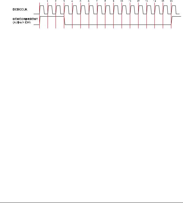
Figure 2-4 illustrates an example drive 0 waveform for an active HIGH output, at 3/16 duty cycle with freq0 (f/16) selected.
Figure 2-4 Example drive 0 waveform
ARM DDI 0147D |
© Copyright ARM Limited 1999. All rights reserved. |
2-9 |

Functional Overview
2-10 |
© Copyright ARM Limited 1999. All rights reserved. |
ARM DDI 0147D |