

Chapter 1
Introduction
This chapter introduces the ARM PrimeCell DC-DC Converter Interface (PL160) and contains the following sections:
•About the ARM PrimeCell DC-DC Converter Interface (PL160) on page 1-2
•AMBA compatibility on page 1-4.
ARM DDI 0147D |
© Copyright ARM Limited 1999. All rights reserved. |
1-1 |
Introduction
1.1About the ARM PrimeCell DC-DC Converter Interface (PL160)
The PrimeCell DC-DC Converter Interface is an Advanced Microcontroller Bus Architecture (AMBA) compliant System-on-a-Chip peripheral that is developed, tested and licensed by ARM.
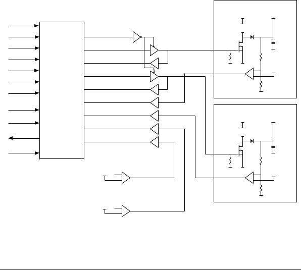
The PrimeCell DC-DC Converter Interface is an AMBA slave module, and connects to the Advanced Peripheral Bus (APB). The PrimeCell DC-DC Converter Interface can be used to implement a configurable dual-output, Pulse Width Modulation (PWM) power converter. Figure 1-1 illustrates a typical interconnection scheme for a PWM controller using the PrimeCell DC-DC Converter Interface.
PCLK
DCDCCLK
BnRES
nDCDCRST
PSEL
PENABLE
PWRITE
PADDR[7:2]
PWDATA[7:0]
PRDATA[7:0]
SCANMODE
DC-DC
Converter
Interface
PAD CONNECTIONS
DCDCDRIVEOE nDCDCDRIVEOE
DCDCDRIVE1OUT |
XDRIVE1 |
|
|
|
|
DCDCDRIVE1IN |
|
|
DCDCDRIVE0OUT |
XDRIVE0 |
|
|
|
|
DCDCDRIVE0IN |
|
|
DCDCFB1 |
|
XFB1 |
|
|
|
DCDCFB0 |
|
XFB0 |
|
|
|
DCDCDR1SEL |
|
XDR1SEL |
|
|
|
DCDCDR0SEL |
|
XDR0SEL |
PSU 1 monitoring |
|
|
Vref |
+ |
|
|
- |
|
PSU 2 monitoring |
|
|
Vref |
+ |
|
|
- |
|
DC-DC Converter 2
VDD |
V2+ |
INDUCTOR 
 L
L
DIODE + C
|
GND |
R |
R |
GND GND |
|
+ |
Vref |
- |
|
|
R |
|
GND |
DC-DC Converter 1
VDD |
V1+ |
INDUCTOR 
 L
L
DIODE + C
|
GND |
R |
R |
GND GND |
|
+ |
Vref |
- |
|
|
R |
|
GND |
Figure 1-1 PrimeCell DC-DC Converter Interface connections diagram
1-2 |
© Copyright ARM Limited 1999. All rights reserved. |
ARM DDI 0147D |

Introduction
1.1.1Features of the PrimeCell DC-DC Converter Interface
The features of the PrimeCell DC-DC Converter Interface are:
•Compliance to the AMBA Specification (Rev 2.0) onwards for easy integration into System-on-a-Chip (SoC) implementation.
•Dual PWM drive outputs, with independent closed loop feedback.
•Software programmable configuration of one of four output frequencies (each being a fixed divide of the input clock). The selectable divide factors are 16, 32, 128, or 304.
•Software programmable configuration of duty cycle from 0 to 15/16, in intervals of 1/16.
•Output polarity (that is, positive or negative voltage generation) is hardware-configured during power-on reset via the polarity select inputs.
•Each PWM drive output can be dynamically switched to one of a pair of preprogrammed frequency/duty cycle combinations via external pins.
ARM DDI 0147D |
© Copyright ARM Limited 1999. All rights reserved. |
1-3 |