- •Preface
- •About this document
- •Feedback
- •1 Introduction to the AMBA Buses
- •1.1 Overview of the AMBA specification
- •1.1.2 Advanced System Bus (ASB)
- •1.1.3 Advanced Peripheral Bus (APB)
- •1.2 Objectives of the AMBA specification
- •1.4 Terminology
- •1.5 Introducing the AMBA AHB
- •1.6 Introducing the AMBA ASB
- •1.7 Introducing the AMBA APB
- •1.8 Choosing the right bus for your system
- •1.8.1 Choice of system bus
- •1.8.2 System bus and peripheral bus
- •1.8.3 When to use AMBA AHB/ASB or APB
- •1.9 Notes on the AMBA specification
- •1.9.1 Technology independence
- •1.9.2 Electrical characteristics
- •1.9.3 Timing specification
- •2 AMBA Signals
- •2.1 AMBA signal names
- •2.1.1 AHB signal prefixes
- •2.1.2 ASB signal prefixes
- •2.1.3 APB signal prefixes
- •2.2 AMBA AHB signal list
- •2.3 AMBA ASB signal list
- •2.4 AMBA APB signal list
- •3 AMBA AHB
- •3.1 About the AMBA AHB
- •3.2 Bus interconnection
- •3.3 Overview of AMBA AHB operation
- •3.4 Basic transfer
- •3.5 Transfer type
- •3.6 Burst operation
- •3.6.1 Early burst termination
- •3.7 Control signals
- •3.7.1 Transfer direction
- •3.7.2 Transfer size
- •3.7.3 Protection control
- •3.8 Address decoding
- •3.9 Slave transfer responses
- •3.9.1 Transfer done
- •3.9.2 Transfer response
- •3.9.4 Error response
- •3.9.5 Split and retry
- •3.10 Data buses
- •3.10.1 HWDATA[31:0]
- •3.10.2 HRDATA[31:0]
- •3.10.3 Endianness
- •3.11 Arbitration
- •3.11.1 Signal description
- •3.11.2 Requesting bus access
- •3.11.3 Granting bus access
- •3.11.4 Early burst termination
- •3.11.5 Locked transfers
- •3.11.6 Default bus master
- •3.12 Split transfers
- •3.12.1 Split transfer sequence
- •3.12.2 Multiple split transfers
- •3.12.3 Preventing deadlock
- •3.12.4 Bus handover with split transfers
- •3.13 Reset
- •3.14 About the AHB data bus width
- •3.15 Implementing a narrow slave on a wider bus
- •3.16 Implementing a wide slave on a narrow bus
- •3.16.1 Masters
- •3.17 About the AHB AMBA components
- •3.18 AHB bus slave
- •3.18.1 Interface diagram
- •3.18.2 Timing diagrams
- •3.18.3 Timing parameters
- •3.19 AHB bus master
- •3.19.1 Interface diagram
- •3.19.2 Bus master timing diagrams
- •3.19.3 Timing parameters
- •3.20 AHB arbiter
- •3.20.1 Interface diagram
- •3.20.2 Timing diagrams
- •3.20.3 Timing parameters
- •3.21 AHB decoder
- •3.21.1 Interface diagram
- •3.21.2 Timing diagram
- •3.21.3 Timing parameter
- •4 AMBA ASB
- •4.1 About the AMBA ASB
- •4.1.2 AMBA ASB and APB
- •4.2 AMBA ASB description
- •4.3 ASB transfers
- •4.3.1 Nonsequential transfer
- •4.3.2 Sequential transfer
- •4.4 Address decode
- •4.5 Transfer response
- •4.6.1 Arbiter
- •4.6.2 Bus master handover
- •4.6.3 Default bus master
- •4.6.4 Locked transfers
- •4.7 Reset operation
- •4.7.1 Exit from reset
- •4.8 Description of ASB signals
- •4.8.1 Clock
- •4.8.2 Reset
- •4.8.3 Transfer type
- •4.8.4 Address and control information
- •4.8.5 Address bus
- •4.8.6 Transfer direction
- •4.8.7 Transfer size
- •4.8.8 Protection information
- •4.8.9 Address and control signal timing
- •4.8.10 Tristate enable of address and control signals
- •4.8.11 Slave select signals
- •4.8.12 Transfer response
- •4.8.13 Data bus
- •4.8.14 Arbitration signals
- •4.9 About the ASB AMBA components
- •4.10 ASB bus slave
- •4.10.1 Interface diagram
- •4.10.2 Bus slave interface description
- •4.10.3 Timing diagrams
- •4.10.4 Timing parameters
- •4.11 ASB bus master
- •4.11.1 Interface diagram
- •4.11.2 Bus master interface description
- •4.11.3 Bus interface state machine
- •4.11.4 Bus master timing diagrams
- •4.11.5 Timing parameters
- •4.12 ASB decoder
- •4.12.1 Interface diagram
- •4.12.2 Decoder description
- •4.12.3 Timing diagrams
- •4.12.4 Timing parameters
- •4.13 ASB arbiter
- •4.13.1 Interface diagram
- •4.13.2 Arbiter description
- •4.13.3 Timing diagrams
- •4.13.4 Timing parameters
- •5 AMBA APB
- •5.1 About the AMBA APB
- •5.2 APB specification
- •5.2.1 State diagram
- •5.2.2 Write transfer
- •5.2.3 Read transfer
- •5.3 About the APB AMBA components
- •5.4 APB bridge
- •5.4.1 Interface diagram
- •5.4.2 APB bridge description
- •5.4.3 Timing diagrams
- •5.4.4 Timing parameters
- •5.5 APB slave
- •5.5.1 Interface diagram
- •5.5.2 APB slave description
- •5.5.3 Timing diagrams
- •5.5.4 Timing parameters
- •5.6 Interfacing APB to AHB
- •5.6.1 Read transfers
- •5.6.2 Write transfers
- •5.6.3 Back to back transfers
- •5.6.4 Tristate data bus implementations
- •5.7 Interfacing APB to ASB
- •5.7.1 Write transfer
- •5.7.2 Read transfer
- •5.8 Interfacing rev D APB peripherals to rev 2.0 APB
- •6 AMBA Test Methodology
- •6.1 About the AMBA test interface
- •6.2 External interface
- •6.2.1 Test bus request A
- •6.2.2 Test bus request B
- •6.2.3 Test acknowledge
- •6.2.4 Test clock
- •6.2.5 Test bus
- •6.3 Test vector types
- •6.4 Test interface controller
- •6.4.1 Test transfer parameters
- •6.4.2 Incremental addressing
- •6.4.3 Entering test mode
- •6.4.4 Address vectors
- •6.4.5 Control vector
- •6.4.6 Write test vectors
- •6.4.7 Read test vectors
- •6.4.8 Burst vectors
- •6.4.9 Changing a burst direction
- •6.4.10 Exiting test mode
- •6.5 The AHB Test Interface Controller
- •6.5.1 Control vector
- •6.6 Example AMBA AHB test sequences
- •6.6.1 Entering test mode
- •6.6.2 Write test vectors
- •6.6.3 Read transfers
- •6.6.4 Control vector
- •6.6.5 Burst vectors
- •6.6.7 Exiting test mode
- •6.7 The ASB test interface controller
- •6.7.1 Control vector bit definitions
- •6.8 Example AMBA ASB test sequences
- •6.8.1 Entering test mode
- •6.8.2 Address vectors
- •6.8.3 Control vectors
- •6.8.4 Write test vectors
- •6.8.5 Changing burst direction
- •6.8.6 Exiting test mode
AMBA APB
5.6Interfacing APB to AHB
Interfacing the AMBA APB to the AHB is described in:
•Read transfers
•Write transfers on page 5-16
•Back to back transfers on page 5-18
•Tristate data bus implementations on page 5-19.
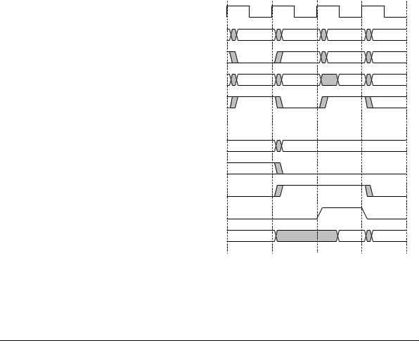
5.6.1Read transfers
Figure 5-9 illustrates a read transfer. |
|
|
|
|
T1 |
T2 |
T3 |
T4 |
T5 |
HADDR |
Addr 1 |
|
|
|
|
|
|
|
|
HWRITE |
|
|
|
|
HRDATA |
|
|
Data 1 |
|
HREADY |
|
|
|
|
PADDR |
|
Addr 1 |
|
|
PWRITE |
|
|
|
|
PSEL |
|
|
|
|
PENABLE |
|
|
|
|
PRDATA |
|
|
Data 1 |
|
Figure 5-9 Read transfer to AHB
5-14 |
© Copyright ARM Limited 1999. All rights reserved. |
ARM IHI 0011A |
AMBA APB
The transfer starts on the AHB at time T1 and the address is sampled by the APB bridge at T2. If the transfer is for the peripheral bus then this address is broadcast and the appropriate peripheral select signal is generated. This first cycle on the peripheral bus is called the SETUP cycle, this is followed by the ENABLE cycle, when the PENABLE signal is asserted.
During the ENABLE cycle the peripheral must provide the read data. Normally it will be possible to route this read data directly back to the AHB, where the bus master can sample it on the rising edge of the clock at the end of the ENABLE cycle, which is at time T4 in Figure 5-9.
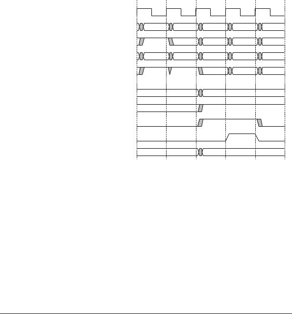
In very high clock frequency systems it may become necessary for the bridge to register the read data at the end of the ENABLE cycle and then for the bridge to drive this back to the AHB bus master in the following cycle. Although this will require an extra wait state for peripheral bus read transfers, it allows the AHB to run at a higher clock frequency, thus resulting in an overall improvement in system performance. A burst of read transfers is shown in Figure 5-10. All read transfers require a single wait state.
T1 |
T2 |
T3 |
T4 |
T5 |
T6 |
T7 |
T8 |
T9 |
T10 |
T11 |
HADDR |
Addr 1 |
Addr 2 |
|
Addr 3 |
|
Addr 4 |
|
|
|
|
|
|
|
|
|
|
|
|
|
|
|
HWRITE |
|
|
|
|
|
|
|
|
|
|
HRDATA |
|
|
Data 1 |
|
Data 2 |
|
Data 3 |
|
Data 4 |
|
|
|
|
|
|
|
|
|
|
|
|
HREADY |
|
|
|
|
|
|
|
|
|
|
PADDR |
|
Addr 1 |
|
Addr 2 |
|
Addr 3 |
|
Addr 4 |
|
|
|
|
|
|
|
|
|
|
|
|
|
PWRITE |
|
|
|
|
|
|
|
|
|
|
PSEL |
|
|
|
|
|
|
|
|
|
|
PENABLE |
|
|
|
|
|
|
|
|
|
|
PRDATA |
|
|
Data 1 |
|
Data 2 |
|
Data 3 |
|
Data 4 |
|
|
|
|
|
|
|
|
|
|
|
Figure 5-10 Burst of read transfers
ARM IHI 0011A |
© Copyright ARM Limited 1999. All rights reserved. |
5-15 |
AMBA APB
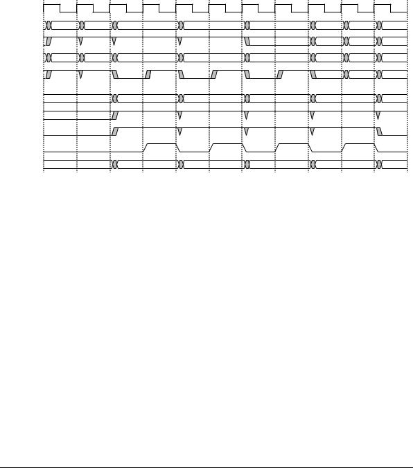
5.6.2Write transfers
Figure 5-11 shows a write transfer.
T1 T2 T3 T4 T5 T6
HADDR |
Addr 1 |
HWRITE |
|
HWDATA |
Data 1 |
HREADY |
|
PADDR |
Addr 1 |
PWRITE |
|
PSEL |
|
PENABLE |
|
PWDATA |
Data 1 |
Figure 5-11 Write transfer from AHB
Single write transfers to the APB can occur with zero wait states. The bridge is responsible for sampling the address and data of the transfer and then holding these values for the duration of the write transfer on the APB.
5-16 |
© Copyright ARM Limited 1999. All rights reserved. |
ARM IHI 0011A |
AMBA APB
A burst of write transfers is shown in Figure 5-12.
T1 |
T2 |
T3 |
T4 |
T5 |
T6 |
T7 |
T8 |
T9 |
T10 |
T11 |
T12 |
HADDR |
Addr 1 |
Addr 2 |
Addr 3 |
|
Addr 4 |
|
|
|
|
|
|
HWRITE |
|
|
|
|
|
|
|
|
|
|
|
HWDATA |
|
Data 1 |
Data 2 |
|
Data 3 |
|
Data 4 |
|
|
|
|
|
|
|
|
|
|
|
|
|
|
|
|
HREADY |
|
|
|
|
|
|
|
|
|
|
|
PADDR |
|
|
Addr 1 |
|
Addr 2 |
|
Addr 3 |
|
Addr 4 |
|
|
|
|
|
|
|
|
|
|
|
|
|
|
PWRITE |
|
|
|
|
|
|
|
|
|
|
|
PSEL |
|
|
|
|
|
|
|
|
|
|
|
PENABLE |
|
|
|
|
|
|
|
|
|
|
|
PWDATA |
|
|
Data 1 |
|
Data 2 |
|
Data 3 |
|
Data 4 |
|
|
|
|
|
|
|
|
|
|
|
|
|
Figure 5-12 Burst of write transfers
While the first transfer can complete with zero wait states, subsequent transfers to the peripheral bus will require a single wait state for each transfer performed.
It is necessary for the bridge to contain two address registers, in order that the bridge can sample the address of the next transfer while the current transfer continues on the peripheral bus.
ARM IHI 0011A |
© Copyright ARM Limited 1999. All rights reserved. |
5-17 |