- •Preface
- •About this document
- •Feedback
- •1 Introduction to the AMBA Buses
- •1.1 Overview of the AMBA specification
- •1.1.2 Advanced System Bus (ASB)
- •1.1.3 Advanced Peripheral Bus (APB)
- •1.2 Objectives of the AMBA specification
- •1.4 Terminology
- •1.5 Introducing the AMBA AHB
- •1.6 Introducing the AMBA ASB
- •1.7 Introducing the AMBA APB
- •1.8 Choosing the right bus for your system
- •1.8.1 Choice of system bus
- •1.8.2 System bus and peripheral bus
- •1.8.3 When to use AMBA AHB/ASB or APB
- •1.9 Notes on the AMBA specification
- •1.9.1 Technology independence
- •1.9.2 Electrical characteristics
- •1.9.3 Timing specification
- •2 AMBA Signals
- •2.1 AMBA signal names
- •2.1.1 AHB signal prefixes
- •2.1.2 ASB signal prefixes
- •2.1.3 APB signal prefixes
- •2.2 AMBA AHB signal list
- •2.3 AMBA ASB signal list
- •2.4 AMBA APB signal list
- •3 AMBA AHB
- •3.1 About the AMBA AHB
- •3.2 Bus interconnection
- •3.3 Overview of AMBA AHB operation
- •3.4 Basic transfer
- •3.5 Transfer type
- •3.6 Burst operation
- •3.6.1 Early burst termination
- •3.7 Control signals
- •3.7.1 Transfer direction
- •3.7.2 Transfer size
- •3.7.3 Protection control
- •3.8 Address decoding
- •3.9 Slave transfer responses
- •3.9.1 Transfer done
- •3.9.2 Transfer response
- •3.9.4 Error response
- •3.9.5 Split and retry
- •3.10 Data buses
- •3.10.1 HWDATA[31:0]
- •3.10.2 HRDATA[31:0]
- •3.10.3 Endianness
- •3.11 Arbitration
- •3.11.1 Signal description
- •3.11.2 Requesting bus access
- •3.11.3 Granting bus access
- •3.11.4 Early burst termination
- •3.11.5 Locked transfers
- •3.11.6 Default bus master
- •3.12 Split transfers
- •3.12.1 Split transfer sequence
- •3.12.2 Multiple split transfers
- •3.12.3 Preventing deadlock
- •3.12.4 Bus handover with split transfers
- •3.13 Reset
- •3.14 About the AHB data bus width
- •3.15 Implementing a narrow slave on a wider bus
- •3.16 Implementing a wide slave on a narrow bus
- •3.16.1 Masters
- •3.17 About the AHB AMBA components
- •3.18 AHB bus slave
- •3.18.1 Interface diagram
- •3.18.2 Timing diagrams
- •3.18.3 Timing parameters
- •3.19 AHB bus master
- •3.19.1 Interface diagram
- •3.19.2 Bus master timing diagrams
- •3.19.3 Timing parameters
- •3.20 AHB arbiter
- •3.20.1 Interface diagram
- •3.20.2 Timing diagrams
- •3.20.3 Timing parameters
- •3.21 AHB decoder
- •3.21.1 Interface diagram
- •3.21.2 Timing diagram
- •3.21.3 Timing parameter
- •4 AMBA ASB
- •4.1 About the AMBA ASB
- •4.1.2 AMBA ASB and APB
- •4.2 AMBA ASB description
- •4.3 ASB transfers
- •4.3.1 Nonsequential transfer
- •4.3.2 Sequential transfer
- •4.4 Address decode
- •4.5 Transfer response
- •4.6.1 Arbiter
- •4.6.2 Bus master handover
- •4.6.3 Default bus master
- •4.6.4 Locked transfers
- •4.7 Reset operation
- •4.7.1 Exit from reset
- •4.8 Description of ASB signals
- •4.8.1 Clock
- •4.8.2 Reset
- •4.8.3 Transfer type
- •4.8.4 Address and control information
- •4.8.5 Address bus
- •4.8.6 Transfer direction
- •4.8.7 Transfer size
- •4.8.8 Protection information
- •4.8.9 Address and control signal timing
- •4.8.10 Tristate enable of address and control signals
- •4.8.11 Slave select signals
- •4.8.12 Transfer response
- •4.8.13 Data bus
- •4.8.14 Arbitration signals
- •4.9 About the ASB AMBA components
- •4.10 ASB bus slave
- •4.10.1 Interface diagram
- •4.10.2 Bus slave interface description
- •4.10.3 Timing diagrams
- •4.10.4 Timing parameters
- •4.11 ASB bus master
- •4.11.1 Interface diagram
- •4.11.2 Bus master interface description
- •4.11.3 Bus interface state machine
- •4.11.4 Bus master timing diagrams
- •4.11.5 Timing parameters
- •4.12 ASB decoder
- •4.12.1 Interface diagram
- •4.12.2 Decoder description
- •4.12.3 Timing diagrams
- •4.12.4 Timing parameters
- •4.13 ASB arbiter
- •4.13.1 Interface diagram
- •4.13.2 Arbiter description
- •4.13.3 Timing diagrams
- •4.13.4 Timing parameters
- •5 AMBA APB
- •5.1 About the AMBA APB
- •5.2 APB specification
- •5.2.1 State diagram
- •5.2.2 Write transfer
- •5.2.3 Read transfer
- •5.3 About the APB AMBA components
- •5.4 APB bridge
- •5.4.1 Interface diagram
- •5.4.2 APB bridge description
- •5.4.3 Timing diagrams
- •5.4.4 Timing parameters
- •5.5 APB slave
- •5.5.1 Interface diagram
- •5.5.2 APB slave description
- •5.5.3 Timing diagrams
- •5.5.4 Timing parameters
- •5.6 Interfacing APB to AHB
- •5.6.1 Read transfers
- •5.6.2 Write transfers
- •5.6.3 Back to back transfers
- •5.6.4 Tristate data bus implementations
- •5.7 Interfacing APB to ASB
- •5.7.1 Write transfer
- •5.7.2 Read transfer
- •5.8 Interfacing rev D APB peripherals to rev 2.0 APB
- •6 AMBA Test Methodology
- •6.1 About the AMBA test interface
- •6.2 External interface
- •6.2.1 Test bus request A
- •6.2.2 Test bus request B
- •6.2.3 Test acknowledge
- •6.2.4 Test clock
- •6.2.5 Test bus
- •6.3 Test vector types
- •6.4 Test interface controller
- •6.4.1 Test transfer parameters
- •6.4.2 Incremental addressing
- •6.4.3 Entering test mode
- •6.4.4 Address vectors
- •6.4.5 Control vector
- •6.4.6 Write test vectors
- •6.4.7 Read test vectors
- •6.4.8 Burst vectors
- •6.4.9 Changing a burst direction
- •6.4.10 Exiting test mode
- •6.5 The AHB Test Interface Controller
- •6.5.1 Control vector
- •6.6 Example AMBA AHB test sequences
- •6.6.1 Entering test mode
- •6.6.2 Write test vectors
- •6.6.3 Read transfers
- •6.6.4 Control vector
- •6.6.5 Burst vectors
- •6.6.7 Exiting test mode
- •6.7 The ASB test interface controller
- •6.7.1 Control vector bit definitions
- •6.8 Example AMBA ASB test sequences
- •6.8.1 Entering test mode
- •6.8.2 Address vectors
- •6.8.3 Control vectors
- •6.8.4 Write test vectors
- •6.8.5 Changing burst direction
- •6.8.6 Exiting test mode
AMBA ASB
4.8.13Data bus
The bidirectional data bus, BD[31:0], is used to transfer data between bus masters and slaves. The size and direction of the transfer is given by the control signals, as described in Address and control information on page 4-27.
The data bus must not be driven during the first BCLK LOW phase of a NONSEQUENTIAL transfer. It may be driven, by the appropriate master or slave, at all other times except reset.
During a write transfer:
•the master drives the data bus during all phases of the transfer, except the first BCLK LOW phase of a NONSEQUENTIAL transfer
•the slave does not drive the bus. During a read transfer:
•The master does not drive the data bus.
•The slave must drive the data bus during the last BCLK HIGH phase of the transfer. For the rest of the transfer, the slave may drive the data bus or leave it tristate, with the provision that it is not driven during the first BCLK LOW phase of a NONSEQUENTIAL transfer.
The following diagrams show some examples of how the data bus is driven.
4-40 |
© Copyright ARM Limited 1999. All rights reserved. |
ARM IHI 0011A |
AMBA ASB
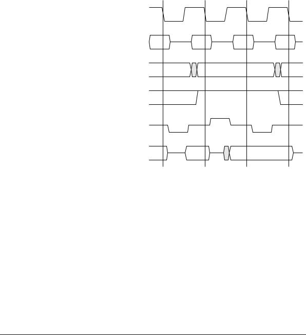
Figure 4-22 shows an example of a NONSEQUENTIAL write transfer.
BCLK |
|
BTRAN[1:0] |
N-TRAN |
BA[31:0] |
Address |
BWRITE |
|
BD[31:0] |
Data |
Figure 4-22 Nonsequential write transfer
The data bus is driven by the bus master, except for the BCLK LOW phase of the first cycle. Not driving the data bus at the start of NONSEQUENTIAL transfers provides a full phase of turnaround between different data bus drivers.
ARM IHI 0011A |
© Copyright ARM Limited 1999. All rights reserved. |
4-41 |
AMBA ASB
When a write transfer is extended using BWAIT, the data remains valid through the BCLK LOW phase of the extra cycles that are required to complete the transfer, as shown in Figure 4-23.
BCLK |
|
BTRAN[1:0] |
N-TRAN |
BA[31:0] |
|
BWRITE |
|
BWAIT |
|
BD[31:0] |
|
Address
Data
Figure 4-23 Extended write transfer
4-42 |
© Copyright ARM Limited 1999. All rights reserved. |
ARM IHI 0011A |
AMBA ASB
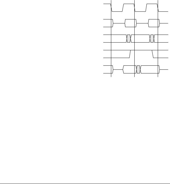
For SEQUENTIAL transfers the bus master may drive data during the LOW phase of BCLK at the start of the transfer, as shown in Figure 4-24. This is permitted as a phase of turnaround is not required for SEQUENTIAL transfers.
BCLK |
|
BTRAN[1:0] |
S-TRAN |
BA[31:0] |
Address |
BWRITE |
|
BD[31:0] |
Data |
Figure 4-24 Sequential write transfer
ARM IHI 0011A |
© Copyright ARM Limited 1999. All rights reserved. |
4-43 |