

AMBA ASB
4.8Description of ASB signals
This section provides more detailed information about all the AMBA ASB signals, including their intended use and phase-accurate timing requirements.
It is necessary to ensure that bus hold cells are provided to prevent floating levels being present on the bus. This is possible because many of the bus signals are shared, and have turnaround periods when there is no active driver.
4.8.1Clock
BCLK is the primary clock, which is used to time all bus transfers. Both edges of the clock are used.
4.8.2Reset
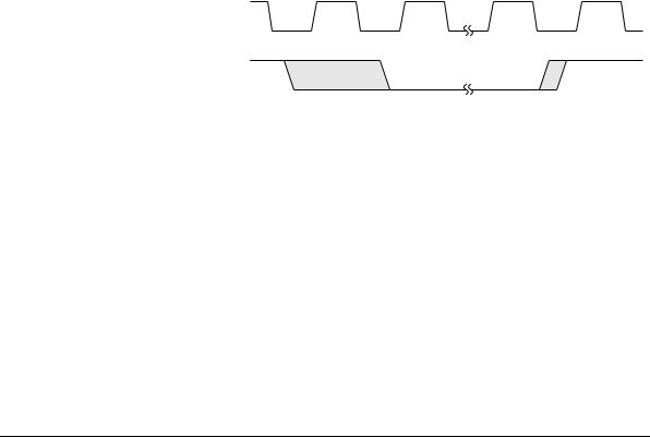
A single active LOW reset signal, BnRES, is supported which is used to reset the bus. The reset signal may be asserted LOW asynchronously during either clock phase, but is always de-asserted during the LOW phase of BCLK.
BCLK
BnRES
Figure 4-12 Reset signal
During reset the following actions occur on the bus:
•the arbiter grants the default bus master
•the default bus master must:
•drive BTRAN to indicate ADDRESS-ONLY transfer
•drive BLOK LOW to allow arbitration.
•all other bus masters tristate shared bus signals
•the decoder must:
•de-assert all slave select signals, DSELx
•provide the appropriate transfer response.
•all slaves tristate shared bus signals.
The BnRES signal may be used to reset the bus during time-out conditions.
ARM IHI 0011A |
© Copyright ARM Limited 1999. All rights reserved. |
4-25 |

AMBA ASB
In the majority of bus masters and slaves the BnRES signal will be used to reset both the bus interface and the main core of the component. However, it is acceptable for some system elements, such as a real-time clock, to use BnRES to only reset the bus interface. Such system elements would typically have a second reset input to allow the component core to be reset at initial power-up and for testing purposes.
4.8.3Transfer type
Before a transfer starts the bus master indicates which type of the transfer it is, using BTRAN[1:0]. The following transfer types can be set:
•ADDRESS-ONLY
•NONSEQUENTIAL
•SEQUENTIAL.
Table 4-1 shows the encoding of the BTRAN[1:0] signals:
Table 4-1 BTRAN encoding
BTRAN
|
|
Transfer type |
Description |
|
[1] |
[0] |
|
|
|
|
|
|
|
|
0 |
0 |
ADDRESS-ONLY |
Used when no data movement is required. The three |
|
|
|
|
main uses for ADDRESS-ONLY transfers are: |
|
|
|
|
• |
for IDLE cycles |
|
|
|
• |
for bus master handover cycles |
|
|
|
• |
for speculative address decoding without |
|
|
|
|
committing to a data transfer. |
|
|
|
|
|
0 |
1 |
- |
Reserved |
|
|
|
|
|
|
1 |
0 |
NONSEQUENTIAL |
Used for single transfers or for the first transfer of a |
|
|
|
|
burst. The address of the transfer is unrelated to the |
|
|
|
|
previous bus access. |
|
|
|
|
|
|
1 |
1 |
SEQUENTIAL |
Used for successive transfers in a burst. The address of |
|
|
|
|
a SEQUENTIAL transfer is always related to the |
|
|
|
|
previous transfer. |
|
|
|
|
|
|
From the table it can be deduced that BTRAN[1] can be used to determine that a data transfer is required next cycle.
4-26 |
© Copyright ARM Limited 1999. All rights reserved. |
ARM IHI 0011A |
AMBA ASB
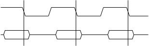
The BTRAN signals are driven by a bus master during the HIGH phase of BCLK when the AGNTx input is HIGH (see Figure 4-13).
BCLK
BTRAN[1:0]
Transfer
type
Figure 4-13 BTRAN timing
In a multi-master system, the bus master that drives BTRAN may change during an extended transfer. Therefore, BTRAN must only be considered valid when the previous transfer has completed, as indicated by BWAIT LOW.
4.8.4Address and control information
The address and control signals are:
•address bus - BA[31:0]
•transfer direction - BWRITE
•transfer size - BSIZE[1:0]
•protection information - BPROT[1:0].
4.8.5Address bus
The 32-bit address bus, BA[31:0], provides the address of the transfer. All transfers are memory-mapped and therefore all memory and peripherals within the system must have an address range within which they are accessed. The decoder uses the address bus (usually the higher order bits) to determine which bus slave is to be accessed.
4.8.6Transfer direction
The BWRITE signal is used to indicate the direction of the transfer (see Table 4-2). When BWRITE is LOW the transfer is a read access and when BWRITE is HIGH the transfer is a write access.
|
|
Table 4-2 BWRITE encoding |
|
|
|
|
BWRITE |
Transfer direction |
|
|
|
|
0 |
Read transfer |
|
|
|
|
1 |
Write transfer |
|
|
|
|
|
|
ARM IHI 0011A |
© Copyright ARM Limited 1999. All rights reserved. |
4-27 |

AMBA ASB
4.8.7Transfer size
BSIZE[1:0] encodes the size of a transfer (see Table 4-3). Byte, halfword and word are all defined, with the final encoding being reserved for future use.
|
|
Table 4-3 BSIZE encoding |
|
|
|
|
BSIZE |
|
|
|
Transfer width |
[1] |
[0] |
|
|
|
|
0 |
0 |
Byte (8 bits) |
|
|
|
0 |
1 |
Halfword (16 bits) |
|
|
|
1 |
0 |
Word (32 bits) |
|
|
|
1 |
1 |
Reserved |
|
|
|
When performing transfers that are narrower than the data bus, such as a byte or halfword transfer, the bus master may replicate the data across the bus, making the bus master effectively bi-endian. When responding to read cycles, a typical slave will not replicate the data on the bus and therefore it is important that the master is expecting data on the same byte lane as that which the slave is driving.
4.8.8Protection information
The bus master may use the BPROT signals to provide additional information about the transfer it is performing (see Table 4-4). This information is primarily intended for use by the decoder when it is acting as a bus protection unit and the majority of bus slaves will not use these signals.
|
|
Table 4-4 BPROT encoding |
|
|
|
BPROT |
|
|
|
|
Transfer privilege |
[1] |
[0] |
|
|
|
|
- |
0 |
Opcode fetch |
|
|
|
- |
1 |
Data access |
|
|
|
0 |
- |
User access |
|
|
|
1 |
- |
Privileged access |
|
|
|
4-28 |
© Copyright ARM Limited 1999. All rights reserved. |
ARM IHI 0011A |