
- •Preface
- •About this document
- •Feedback
- •1 Introduction to the AMBA Buses
- •1.1 Overview of the AMBA specification
- •1.1.2 Advanced System Bus (ASB)
- •1.1.3 Advanced Peripheral Bus (APB)
- •1.2 Objectives of the AMBA specification
- •1.4 Terminology
- •1.5 Introducing the AMBA AHB
- •1.6 Introducing the AMBA ASB
- •1.7 Introducing the AMBA APB
- •1.8 Choosing the right bus for your system
- •1.8.1 Choice of system bus
- •1.8.2 System bus and peripheral bus
- •1.8.3 When to use AMBA AHB/ASB or APB
- •1.9 Notes on the AMBA specification
- •1.9.1 Technology independence
- •1.9.2 Electrical characteristics
- •1.9.3 Timing specification
- •2 AMBA Signals
- •2.1 AMBA signal names
- •2.1.1 AHB signal prefixes
- •2.1.2 ASB signal prefixes
- •2.1.3 APB signal prefixes
- •2.2 AMBA AHB signal list
- •2.3 AMBA ASB signal list
- •2.4 AMBA APB signal list
- •3 AMBA AHB
- •3.1 About the AMBA AHB
- •3.2 Bus interconnection
- •3.3 Overview of AMBA AHB operation
- •3.4 Basic transfer
- •3.5 Transfer type
- •3.6 Burst operation
- •3.6.1 Early burst termination
- •3.7 Control signals
- •3.7.1 Transfer direction
- •3.7.2 Transfer size
- •3.7.3 Protection control
- •3.8 Address decoding
- •3.9 Slave transfer responses
- •3.9.1 Transfer done
- •3.9.2 Transfer response
- •3.9.4 Error response
- •3.9.5 Split and retry
- •3.10 Data buses
- •3.10.1 HWDATA[31:0]
- •3.10.2 HRDATA[31:0]
- •3.10.3 Endianness
- •3.11 Arbitration
- •3.11.1 Signal description
- •3.11.2 Requesting bus access
- •3.11.3 Granting bus access
- •3.11.4 Early burst termination
- •3.11.5 Locked transfers
- •3.11.6 Default bus master
- •3.12 Split transfers
- •3.12.1 Split transfer sequence
- •3.12.2 Multiple split transfers
- •3.12.3 Preventing deadlock
- •3.12.4 Bus handover with split transfers
- •3.13 Reset
- •3.14 About the AHB data bus width
- •3.15 Implementing a narrow slave on a wider bus
- •3.16 Implementing a wide slave on a narrow bus
- •3.16.1 Masters
- •3.17 About the AHB AMBA components
- •3.18 AHB bus slave
- •3.18.1 Interface diagram
- •3.18.2 Timing diagrams
- •3.18.3 Timing parameters
- •3.19 AHB bus master
- •3.19.1 Interface diagram
- •3.19.2 Bus master timing diagrams
- •3.19.3 Timing parameters
- •3.20 AHB arbiter
- •3.20.1 Interface diagram
- •3.20.2 Timing diagrams
- •3.20.3 Timing parameters
- •3.21 AHB decoder
- •3.21.1 Interface diagram
- •3.21.2 Timing diagram
- •3.21.3 Timing parameter
- •4 AMBA ASB
- •4.1 About the AMBA ASB
- •4.1.2 AMBA ASB and APB
- •4.2 AMBA ASB description
- •4.3 ASB transfers
- •4.3.1 Nonsequential transfer
- •4.3.2 Sequential transfer
- •4.4 Address decode
- •4.5 Transfer response
- •4.6.1 Arbiter
- •4.6.2 Bus master handover
- •4.6.3 Default bus master
- •4.6.4 Locked transfers
- •4.7 Reset operation
- •4.7.1 Exit from reset
- •4.8 Description of ASB signals
- •4.8.1 Clock
- •4.8.2 Reset
- •4.8.3 Transfer type
- •4.8.4 Address and control information
- •4.8.5 Address bus
- •4.8.6 Transfer direction
- •4.8.7 Transfer size
- •4.8.8 Protection information
- •4.8.9 Address and control signal timing
- •4.8.10 Tristate enable of address and control signals
- •4.8.11 Slave select signals
- •4.8.12 Transfer response
- •4.8.13 Data bus
- •4.8.14 Arbitration signals
- •4.9 About the ASB AMBA components
- •4.10 ASB bus slave
- •4.10.1 Interface diagram
- •4.10.2 Bus slave interface description
- •4.10.3 Timing diagrams
- •4.10.4 Timing parameters
- •4.11 ASB bus master
- •4.11.1 Interface diagram
- •4.11.2 Bus master interface description
- •4.11.3 Bus interface state machine
- •4.11.4 Bus master timing diagrams
- •4.11.5 Timing parameters
- •4.12 ASB decoder
- •4.12.1 Interface diagram
- •4.12.2 Decoder description
- •4.12.3 Timing diagrams
- •4.12.4 Timing parameters
- •4.13 ASB arbiter
- •4.13.1 Interface diagram
- •4.13.2 Arbiter description
- •4.13.3 Timing diagrams
- •4.13.4 Timing parameters
- •5 AMBA APB
- •5.1 About the AMBA APB
- •5.2 APB specification
- •5.2.1 State diagram
- •5.2.2 Write transfer
- •5.2.3 Read transfer
- •5.3 About the APB AMBA components
- •5.4 APB bridge
- •5.4.1 Interface diagram
- •5.4.2 APB bridge description
- •5.4.3 Timing diagrams
- •5.4.4 Timing parameters
- •5.5 APB slave
- •5.5.1 Interface diagram
- •5.5.2 APB slave description
- •5.5.3 Timing diagrams
- •5.5.4 Timing parameters
- •5.6 Interfacing APB to AHB
- •5.6.1 Read transfers
- •5.6.2 Write transfers
- •5.6.3 Back to back transfers
- •5.6.4 Tristate data bus implementations
- •5.7 Interfacing APB to ASB
- •5.7.1 Write transfer
- •5.7.2 Read transfer
- •5.8 Interfacing rev D APB peripherals to rev 2.0 APB
- •6 AMBA Test Methodology
- •6.1 About the AMBA test interface
- •6.2 External interface
- •6.2.1 Test bus request A
- •6.2.2 Test bus request B
- •6.2.3 Test acknowledge
- •6.2.4 Test clock
- •6.2.5 Test bus
- •6.3 Test vector types
- •6.4 Test interface controller
- •6.4.1 Test transfer parameters
- •6.4.2 Incremental addressing
- •6.4.3 Entering test mode
- •6.4.4 Address vectors
- •6.4.5 Control vector
- •6.4.6 Write test vectors
- •6.4.7 Read test vectors
- •6.4.8 Burst vectors
- •6.4.9 Changing a burst direction
- •6.4.10 Exiting test mode
- •6.5 The AHB Test Interface Controller
- •6.5.1 Control vector
- •6.6 Example AMBA AHB test sequences
- •6.6.1 Entering test mode
- •6.6.2 Write test vectors
- •6.6.3 Read transfers
- •6.6.4 Control vector
- •6.6.5 Burst vectors
- •6.6.7 Exiting test mode
- •6.7 The ASB test interface controller
- •6.7.1 Control vector bit definitions
- •6.8 Example AMBA ASB test sequences
- •6.8.1 Entering test mode
- •6.8.2 Address vectors
- •6.8.3 Control vectors
- •6.8.4 Write test vectors
- •6.8.5 Changing burst direction
- •6.8.6 Exiting test mode

AMBA AHB
3.8Address decoding
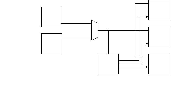
A central address decoder is used to provide a select signal, HSELx, for each slave on the bus. The select signal is a combinatorial decode of the high-order address signals, and simple address decoding schemes are encouraged to avoid complex decode logic and to ensure high-speed operation.
A slave must only sample the address and control signals and HSELx when HREADY is HIGH, indicating that the current transfer is completing. Under certain circumstances it is possible that HSELx will be asserted when HREADY is LOW, but the selected slave will have changed by the time the current transfer completes.
The minimum address space that can be allocated to a single slave is 1kB. All bus masters are designed such that they will not perform incrementing transfers over a 1kB boundary, thus ensuring that a burst never crosses an address decode boundary.
In the case where a system design does not contain a completely filled memory map an additional default slave should be implemented to provide a response when any of the nonexistent address locations are accessed. If a NONSEQUENTIAL or SEQUENTIAL transfer is attempted to a nonexistent address location then the default slave should provide an ERROR response. IDLE or BUSY transfers to nonexistent locations should result in a zero wait state OKAY response. Typically the default slave functionality will be implemented as part of the central address decoder.
Figure 3-12 shows a typical address decoding system and the slave select signals.
|
|
|
Slave |
Master |
|
|
# 1 |
|
|
|
|
# 1 |
HADDR_M1[31:0] |
|
|
|
|
|
|
|
HADDR to all slaves |
|
|
|
HADDR_M2[31:0] |
|
Slave |
Master |
|
|
# 2 |
Address and |
|
|
|
# 2 |
control mux |
|
|
|
|
HSEL_S1 |
|
|
Decoder |
HSEL_S2 |
Slave |
|
HSEL_S3 |
# 3 |
|
|
|
Figure 3-12 Slave select signals
ARM IHI 0011A |
© Copyright ARM Limited 1999. All rights reserved. |
3-19 |