

AMBA AHB
3.2Bus interconnection
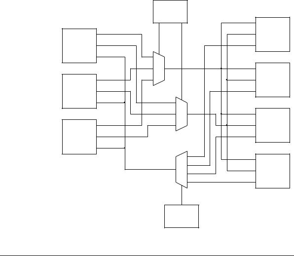
The AMBA AHB bus protocol is designed to be used with a central multiplexor interconnection scheme. Using this scheme all bus masters drive out the address and control signals indicating the transfer they wish to perform and the arbiter determines which master has its address and control signals routed to all of the slaves. A central decoder is also required to control the read data and response signal multiplexor, which selects the appropriate signals from the slave that is involved in the transfer.
Figure 3-2 illustrates the structure required to implement an AMBA AHB design with three masters and four slaves.
|
|
Arbiter |
|
|
|
|
|
HADDR |
|
|
HADDR |
|
HWDATA |
Slave |
Master |
HWDATA |
|
HRDATA |
# 1 |
|
|
|||
# 1 |
HRDATA |
|
|
|
|
|
|
|
|
|
|
|
HADDR |
|
|
HADDR |
|
HWDATA |
Slave |
Master |
HWDATA |
|
HRDATA |
# 2 |
Address and |
|
|||
# 2 |
HRDATA |
control mux |
|
|
|
|
|
|
|
|
|
|
HADDR |
|
|
HADDR |
|
HWDATA |
Slave |
Master |
HWDATA |
|
HRDATA |
# 3 |
Write data mux |
|
|||
# 3 |
HRDATA |
|
|
|
|
Read data mux |
|
|
|
|
|
|
|
|
|
|
|
HADDR |
|
|
|
|
HWDATA |
Slave |
|
|
|
HRDATA |
# 4 |
|
|
|
|
|
|
|
Decoder |
|
|
Figure 3-2 Multiplexor interconnection
3-4 |
© Copyright ARM Limited 1999. All rights reserved. |
ARM IHI 0011A |

AMBA AHB
3.3Overview of AMBA AHB operation
Before an AMBA AHB transfer can commence the bus master must be granted access to the bus. This process is started by the master asserting a request signal to the arbiter. Then the arbiter indicates when the master will be granted use of the bus.
A granted bus master starts an AMBA AHB transfer by driving the address and control signals. These signals provide information on the address, direction and width of the transfer, as well as an indication if the transfer forms part of a burst. Two different forms of burst transfers are allowed:
•incrementing bursts, which do not wrap at address boundaries
•wrapping bursts, which wrap at particular address boundaries.
A write data bus is used to move data from the master to a slave, while a read data bus is used to move data from a slave to the master.
Every transfer consists of:
•an address and control cycle
•one or more cycles for the data.
The address cannot be extended and therefore all slaves must sample the address during this time. The data, however, can be extended using the HREADY signal. When LOW this signal causes wait states to be inserted into the transfer and allows extra time for the slave to provide or sample data.
During a transfer the slave shows the status using the response signals, HRESP[1:0]:
OKAY |
The OKAY response is used to indicate that the transfer is |
|
progressing normally and when HREADY goes HIGH this shows |
|
the transfer has completed successfully. |
ERROR |
The ERROR response indicates that a transfer error has occurred |
|
and the transfer has been unsuccessful. |
RETRY and SPLIT |
Both the RETRY and SPLIT transfer responses indicate that the |
|
transfer cannot complete immediately, but the bus master should |
|
continue to attempt the transfer. |
In normal operation a master is allowed to complete all the transfers in a particular burst before the arbiter grants another master access to the bus. However, in order to avoid excessive arbitration latencies it is possible for the arbiter to break up a burst and in such cases the master must re-arbitrate for the bus in order to complete the remaining transfers in the burst.
ARM IHI 0011A |
© Copyright ARM Limited 1999. All rights reserved. |
3-5 |
AMBA AHB
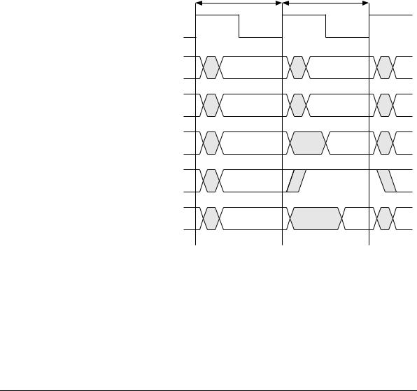
3.4Basic transfer
An AHB transfer consists of two distinct sections:
•The address phase, which lasts only a single cycle.
•The data phase, which may require several cycles. This is achieved using the HREADY signal.
Figure 3-3 shows the simplest transfer, one with no wait states.
Address phase |
Data phase |
HCLK |
|
|
HADDR[31:0] |
A |
|
Control |
Control |
|
HWDATA[31:0] |
Data |
|
(A) |
||
|
||
HREADY |
|
|
HRDATA[31:0] |
Data |
|
(A) |
||
|
||
|
Figure 3-3 Simple transfer |
In a simple transfer with no wait states:
•The master drives the address and control signals onto the bus after the rising edge of HCLK.
•The slave then samples the address and control information on the next rising edge of the clock.
3-6 |
© Copyright ARM Limited 1999. All rights reserved. |
ARM IHI 0011A |
AMBA AHB
•After the slave has sampled the address and control it can start to drive the appropriate response and this is sampled by the bus master on the third rising edge of the clock.
This simple example demonstrates how the address and data phases of the transfer occur during different clock periods. In fact, the address phase of any transfer occurs during the data phase of the previous transfer. This overlapping of address and data is fundamental to the pipelined nature of the bus and allows for high performance operation, while still providing adequate time for a slave to provide the response to a transfer.
A slave may insert wait states into any transfer, as shown in Figure 3-4, which extends the transfer allowing additional time for completion.
Address phase |
Data phase |
HCLK
HADDR[31:0]
Control
HWDATA[31:0]
HREADY
HRDATA[31:0]
A
Control
Data
(A)
Data
(A)
Figure 3-4 Transfer with wait states
Note
For write operations the bus master will hold the data stable throughout the extended cycles.
For read transfers the slave does not have to provide valid data until the transfer is about to complete.
ARM IHI 0011A |
© Copyright ARM Limited 1999. All rights reserved. |
3-7 |
AMBA AHB
When a transfer is extended in this way it will have the side-effect of extending the address phase of the following transfer. This is illustrated in Figure 3-5 which shows three transfers to unrelated addresses, A, B & C.
HCLK
HADDR[31:0]
Control
HWDATA[31:0]
HREADY
HRDATA[31:0]
A |
B |
C |
|
Control |
Control |
Control |
|
(A) |
(B) |
(C) |
|
|
Data |
Data |
Data |
|
(A) |
(B) |
(C) |
Data |
Data |
Data |
(A) |
(B) |
(C) |
Figure 3-5 Multiple transfers
In Figure 3-5:
•the transfers to addresses A and C are both zero wait state
•the transfer to address B is one wait state
•extending the data phase of the transfer to address B has the effect of extending the address phase of the transfer to address C.
3-8 |
© Copyright ARM Limited 1999. All rights reserved. |
ARM IHI 0011A |