- •Table of Contents
- •1.1. Introduction
- •1.2. Problems
- •2. Behavior and Structure models
- •2.1. Introduction
- •2.2. Problems
- •3. State Machines and Programmable Logic Devices
- •3.1. Introduction
- •3.2. Mealy and Moore State Machines
- •3.4. Problems
- •4. Digital Device Modeling
- •4.1. Introduction
- •4.2. SRAM Memory
- •4.3. VHDL SRAM Memory Design
- •4.5. Problems
- •5.1. Introduction
- •5.2. VHDL Features
- •5.3. ALU Functions
- •5.6. Problems
- •6.1. Introduction
- •6.2. Instruction Set Architecture (ISA)
- •6.3. A Computer Architecture Implementation
- •6.5. Problems
- •7. Appendices
- •7.1. Install Warp on PC
Digital Design VHDL Laboratory
4.VHDL - Hardware Design Software Approach
pepe, 4/30/96
signal datain, dataout: bit_vector (word_width-1 downto 0); signal memory_word: memory_elmt;
signal w: integer; begin
-- Memory read cycle
process (nce) begin
ReadMemory(nce, nwrite, address, memory_word, dataout); end process;
-- Memory write cycle
process (nce) begin
WriteMemory(nce, nwrite, address, memory_word, datain); end process;
-- Tristate input and output
bif0: bufoe port map(dataout(0), nwrite, bidata(0), datain(0)); bif1: bufoe port map(dataout(1), nwrite, bidata(1), datain(1));
end sram0arch;
Listing 4-1. SRAM VHDL Code
4.5 Problems
1)The Cypress Warp tool uses the time unit tick. Figure 4-2 shows an example of tick value 68. From Figure 4-1, use the Warp simulator to determine the minimum times for signals Tnce2datain, Tnce2nwr and Tnce2addr that produce a valid Tnce2dataout. Also, what is the value of Tnce2dataout?
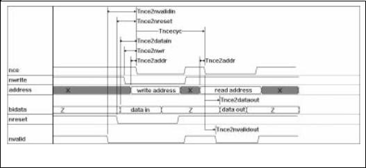
2)The timing diagram in Figure 4-3 below shows a modified SRAM that contains an extra field for storing a valid bit. This memory is to be named SRAMvc (SRAM with valid control) memory. To put data into a memory location, the signal nvalid has to be set to zero prior to signal nce’s going during the SRAMvc reading cycle, if the signal nvalid at the requested address location is high, bidata should output zero. During the SRAMvc writing cycle, data will write into the memory along with the nvalid signal. If the signal nvalid is high, the maximum data value (all bits set to one) should write into the corresponding memory location.
Before using SRAMvc, a signal nreset should be applied to invalidate signal nvalid all memory locations (for example, nvalid<=‘0’). In result, all nvalid bits will be set to zero, and all bidata value will be set to max. See Figure 4-3 for the timing relationship of nreset and nce.
Construct SRAMvc using VHDL and prove its functional by simulation. The simulator should produce timing waveforms similar to those shown in Figure 4-3.
From the simulation, find all the timing parameters in Figure 4-3 based on the simulation of your SRAMvc VHDL model.
30 |
Copyright 1996, CERL / EE, V1.00 |

Digital Design VHDL Laboratory 4.VHDL - Hardware Design Software Approach pepe, 4/30/96
Figure 4-3. SRAMvc Timing Diagram
31 |
Copyright 1996, CERL / EE, V1.00 |

Digital Design VHDL Laboratory
5.Digital Design using Divide and Conquer
pepe, 4/30/96
5. Digital Design using Divide and Conquer
5.1 Introduction
As the demand for digital system complexity increases, one needs to rely on traditional divide and conquer methodologies for constructing complex digital systems. VHDL contains features that support the divide and conquer technique for designing complex system design.
Some of the VHDL features that that permit the designer to build sub-systems have already been introduced in previous lessons: for example, the use of VHDL component block and procedure and functions statements. In addition, there is a benefit to breaking a large problem into many smaller problems because the solution for each small problem can be reused and applied to other problems similar in nature. For example, the design of an automobile fuel mixer controller might require the use of a two stage 5 bit D flip flop. By coincidence, this same odd device (2-stages, 5-bit D flip flop) is also used inside traffic light controller. One can imagine that the design for this device should not have to be implemented twice, provided the design tool (I.e. VHDL) allows it. This is the concept of hardware reuse, and for a long time it has been employed in the object oriented software world. In this lesson, the VHDL package and library between which support “hardware reuse” will be introduced.
5.2 VHDL features
The use of VHDL component and procedure statements in previous lessons gave the VHDL designer a systematic way of breaking a large and complicated problem into smaller, and simpler problems to solve. The VHDL package clause feature lets the digital designer pack tested digital parts into a library (storage). Then, he/she can use the VHDL keyword use or library to retrieve these parts for any design afterwards. This enables designer to build more complex systems and also encourages the digital design divide and conquer methodologies.
5.3 ALU Functions
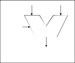
The Arithmetic logic unit (ALU) is the most important part of the computation engine because it directly affects the system performance. All computational arithmetic or logic operations are done in the ALU. Therefore, it is clear that ALU output latency will affect the overall input to output delay. Figure 5-1 shows the general block diagram of an ALU.
Operand 1 |
Operand 2 |
Function Select
ALU
ALU Output
Figure 5-1. ALU Block Diagram
The types of functions built into an ALU depends on the nature of computation. For example, a number crunching ALU such as a digital signal processor (DSP) will devote a good portion of ALU resources for floating point number manipulation such as floating point add, multiply, etc. An intelligent embeded
32 |
Copyright 1996, CERL / EE, V1.00 |

Digital Design VHDL Laboratory
5.Digital Design using Divide and Conquer
pepe, 4/30/96
controller, on the other hand, would probably have an overall balanced arithmetic and logic functions, with emphasis on integer manipulation.
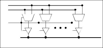
There are many ways to construct an ALU. During the 1980’s, when Large Scale Integration (LSI) Integrated Chip (IC) and Medium Scale Integration IC were popular, bit-slice ALU design was the main technology due to its modularity for LSI and MSI design. The bit-slice design concept was used because it reduced computations to individual bits as to minimize each bit’s overlapping functionality. In the current trend of integrated circuit technology (e.g. VLSI), ALU designers focus less on the ALU’s bit versatility and more towards the its overall speed performance. An ALU design example is shown in Figure 5-2.
Operand 1
Operand 2
F0 |
|
F1 |
|
Fn |
|
|
Function Select
ALU Output
Figure 5-2. An ALU Design
Figure 5-2 is a simplified ALU design, nevertheless, it shows a good overall ALU structure. In the ALU, function boxes, F0, F1, to Fn are dedicated for specified ALU functions such as add, multiply, shift, etc. The inputs to each function box are delivered by two buses, operand1 and operand2. Output of each function box is tapped onto the output bus via tri-state buffers. In addition to the resulting data outputs, there are also ALU flag outputs such as divide by zero, arithmetic overflow, underflow, etc. Each function box is controlled by the control input bits. When functions are similar in nature, for example, left circular and right circular shifts, control bits are used to distinguish these functions.
There are many arithmetic and logic functions that a computer architecture designer might like to put into an ALU. However, due to design requirements and technology limitations the designer must compromise all the factors for an optimal area and speed tradeoff.
5.4 ALU Component Implementation Examples
For simple laboratory work, one might like to design a 4-bit, 2’s complement ALU which consists a 4-bit adder for integer arithmetic, left circular shift, right circular shift, and bitwise AND and OR logic functions.
VHDL supports modular hardware implementation by using the objected oriented software concept of reusability. In VHDL, code or program pieces such as a procedure, function or component can be stored into a library for later use. Whenever the parts are needed, they can be linked into the main VHDL program and reused again. The VHDL feature that supports part reuse is called Package, and it is described in the ALU implementation example.
5.4.1 Ripple Carry Adder Implementation
A ripple carry adder is the simplest adder and it is easiest to build. To implement a 4-bit adder, one starts by paralleling a half adder with full adders. Ripple carry adder implementation can be found in many digital design text books. this laboratory, half adder and full adder components were implemented and
33 |
Copyright 1996, CERL / EE, V1.00 |

Digital Design VHDL Laboratory
5.Digital Design using Divide and Conquer
pepe, 4/30/96
they have been placed inside of the library, Arith_parts_pkg package. The listing of the Arith_parts_pkg package is shown in Section 5.4.2.
In Arith_parts_pkg, components half_adder and full_adder were combined to produce a 4-bit ripple carry adder ripp_adder4. One example of hardware reuse is to test the functionality of ripp_adder4 without reimplementing the same module. This is done by creating a VHDL module, addtest.vhd, which is listed in Section 5.4.3. In file addtest.vhd, after the entity declaration, the line beginning with the VHDL key word use tells the VHDL compiler that all modules (procedure, function, and component) inside of the package iarith_parts_pkg are visible to file addtest.vhd and therefore are available for use.
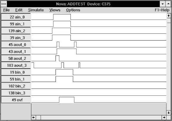
Only the module ripp_adder4 is used structurally inside of the addtest module. Remaining modules such as full_adder and half adder are not shown inside of the addtest module; nevertheless, they were important in building the ripple carry adder ripp_adder4. The test wave form which illustrates the adder’s functionality is shown in Figure 5-3. In Figure 5-3, ain is set to “1111” and bin is set to “0011”. The output aout becomes “0010” with the overflow flag set to 1. Notice the glitches on the at aout lines caused by the asynchronous ain and bin input signals.
Figure 5-3. Ripple Carry Adder Waveform
5.4.2 Package Iarith_parts_pkg Listing
package iarith_parts_pkg is
component half_adder port(signal Ain, Bin: in bit;
signal Cout, Sout: out bit);
end component;
component full_adder
port(signal Cin, Ain, Bin: in bit;
34 |
Copyright 1996, CERL / EE, V1.00 |
Digital Design VHDL Laboratory 5.Digital Design using Divide and Conquer pepe, 4/30/96
signal Cout, Sout: out bit); end component;
component ripp_adder4
port(signal Ain, Bin: in bit_vector (3 downto 0); signal Sout: out bit_vector (3 downto 0); signal OverFlow: out bit);
end component; end iarith_parts_pkg;
----------------------------------------------------------
-- Half adder component
entity half_adder is port(signal Ain, Bin: in bit;
signal Cout, Sout: out bit); end half_adder;
architecture half_adder_arch of half_adder is
begin
process (Ain, Bin) begin
if Ain='1' and Bin='1' then Sout <= '0';
Cout <= '1'; else
Cout <= '0';
Sout <= Ain or Bin; end if;
end process; end half_adder_arch;
----------------------------------------------------------
-- Full adder component
entity full_adder is
port(signal Cin, Ain, Bin: in bit; signal Cout, Sout: out bit);
end full_adder;
architecture full_adder_arch of full_adder is begin
process (Ain, Bin, Cin) begin
if Ain='1' and Bin='1' and Cin='1' then Sout <= '1';
Cout <= '1'; elsif Cin='0' then
if Ain='1' and Bin='1' then
Sout |
<= '0'; |
Cout |
<= '1'; |
else |
|
Sout |
<= Ain or Bin; |
Cout |
<= '0'; |
end if;
else -- |
Cin='1' and either Ain='1' or Bin='1' |
Sout |
<= not (Ain or Bin); |
Cout <= Ain or Bin; end if;
end process;
end full_adder_arch;
----------------------------------------------------------
35 |
Copyright 1996, CERL / EE, V1.00 |
Digital Design VHDL Laboratory 5.Digital Design using Divide and Conquer pepe, 4/30/96
-- 4 bit adder component
entity ripp_adder4 is
port(signal Ain, Bin: in bit_vector (3 downto 0);
signal Sout: out bit_vector (3 downto 0); signal OverFlow: out bit);
end ripp_adder4;
architecture ripp_adder4_arch of ripp_adder4 is signal Cout: bit_vector (3 downto 1);
begin
ha0: half_adder
port map(Ain=>Ain(0), Bin=>Bin(0),
Cout=>Cout(1), Sout=>Sout(0));
fa1: full_adder
port map(Cin=>Cout(1), Ain=>Ain(1), Bin=>Bin(1), Cout=>Cout(2), Sout=>Sout(1));
fa2: full_adder
port map(Cin=>Cout(2), Ain=>Ain(2), Bin=>Bin(2), Cout=>Cout(3), Sout=>Sout(2));
fa3: full_adder
port map(Cin=>Cout(3), Ain=>Ain(3), Bin=>Bin(3), Cout=>OverFLow, Sout=>Sout(3));
end ripp_adder4_arch;
Listing 5-1. Iarith_parts_pkg VHDL Code Listing
5.4.3 Testadd.vhd Listing
---------------------------------------------------
--to test ripple adder routine using component
--"ripp_adder4" of vhdl file iar.vhd.
---------------------------------------------------
entity addtest is
generic( data_wd: integer := 3);
port ( |
Ain: in bit_vector (data_wd downto 0); |
|
Bin: in bit_vector (data_wd downto 0); |
|
Aout:out bit_vector(data_wd downto 0); |
|
OVF: out bit); |
end addtest; |
|
use work.iarith_parts_pkg.all;
architecture addtest_arch of addtest is
begin
op4: ripp_adder4 port map(Ain, Bin, Aout, OVF);
end;
Listing 5-2. Testadd.vhd VHDL Code Listing
36 |
Copyright 1996, CERL / EE, V1.00 |
Digital Design VHDL Laboratory
5.Digital Design using Divide and Conquer
pepe, 4/30/96
5.4.4 Circular Shifter Implementation
The circular shifter unit is more difficult to implement than simple bitwise logical operations. To make the implementation more challenging, the shifter was implemented in generalized fashion so it could accommodate various bus widths. Again, by applying the concept of reuse, the implementation of the circular shifter was put into a library for test. The library that contains the shifter is called logic_parts_pkg, and the VHDL code is listed in Section 5.4.6. Again, the testing of circular shift logic can be performed similar to the ripple carry adder test. The trace file for doing two right circular shifts on ain bits “0010” is “1000” and is shown in the Section 5.4.5. Notice that the output “1000” took 3 ticks to come out after applying inputs ain and bin. Ain is the bit to be shifted and bin is the shifted value. In the cshift component of logic_parts_pkg, input bit RL was used to indicate shift direction: RL=’0’ for left circular shift and ‘1’ for right circular shift.
5.4.5 Circular Shift Trace Data
NOVA Simulation Printout
File: TEST.psd - View: PINS and REGS
Printout produced: Thu Jun 13 01:46:57 1996
b b a a a a a a a a i i i i i i o o o o n n n n n n u u u u
_ _ _ _ _ _ t t t t 0 1 0 1 2 3 _ _ _ _
| | | | | | 0 1 2 3
| | | | | | | | | |
^^^^^^^^^^^^^^^^^^^^^^^^^^^
0:0 1 0 0 1 0 L L L L
1:0 1 0 0 1 0 L L L L
2:0 1 0 0 1 0 L L L L
3:0 1 0 0 1 0 H L L L
4:0 1 0 0 1 0 H L L L
5:0 1 0 0 1 0 H L L L
6:0 1 0 0 1 0 H L L L
7:0 1 0 0 1 0 H L L L
8:0 1 0 0 1 0 H L L L
9:0 1 0 0 1 0 H L L L
10:0 1 0 0 1 0 H L L L
11:0 1 0 0 1 0 H L L L
12:0 1 0 0 1 0 H L L L
13:0 1 0 0 1 0 H L L L
14:0 1 0 0 1 0 H L L L
Listing 5-3. Circular Shift Trace Listing
5.4.6 Package Logic_parts_pkg Listing
package logic_parts_pkg is component cshift
generic (data_wd: integer:= 3);
port (Ain: in bit_vector (data_wd downto 0); Sin: in bit_vector (1 downto 0); RL : in bit;
Sout: out bit_vector(data_wd downto 0));
end component;
component bAND
port (Ain: in bit_vector (3 downto 0);
Bin: in bit_vector (3 downto 0); Cout: out bit_vector (3 downto 0));
37 |
Copyright 1996, CERL / EE, V1.00 |
Digital Design VHDL Laboratory 5.Digital Design using Divide and Conquer pepe, 4/30/96
end component;
component bOR
port (Ain: in bit_vector (3 downto 0);
Bin: in bit_vector (3 downto 0); Cout: out bit_vector (3 downto 0));
end component;
end logic_parts_pkg;
-- Use Cypress library
use work.bv_math.all; use work.int_math.all;
-----------------------------------------------------
--Circular right or left shift
--Input:
--Ain - Input bits
--Sin - Number of shift
--RL - 0: left circular shift
--1: right circular shift
--Output:
--Sout - Output bits
-----------------------------------------------------
entity cshift is
generic(data_wd: integer := 3);
port( Ain: in bit_vector (data_wd downto 0); Sin: in bit_vector (1 downto 0); RL : in bit;
Sout: out bit_vector(data_wd downto 0));
end cshift;
-----------------------------------------------------
architecture cshift_arch of cshift is
signal temp: bit_vector (data_wd downto 0); begin
process (Ain, Sin, RL) variable i, j, k, l: integer := 0; begin
-- i is the shifted value
for i in 0 to data_wd loop
if i=bv2i(Sin) then
for j in 0 to data_wd loop
-- Find right circular shift index k
if RL='1' then
k := j+(data_wd+1)-i;
-- Find left circular shift index k
else
k := j+i; end if;
38 |
Copyright 1996, CERL / EE, V1.00 |
Digital Design VHDL Laboratory 5.Digital Design using Divide and Conquer pepe, 4/30/96
-- Assign Output
if k > data_wd then
k := k-(data_wd+1); end if;
for l in 0 to data_wd loop if k=l then
temp(l) <= Ain(j); end if;
end loop;
end loop;
end if;
end loop;
Sout <= temp;
end process;
end cshift_arch;
-----------------------------------------------------
-- Bitwise AND
----------------------------------------------------
entity bAND is
port( Ain: in bit_vector (3 downto 0);
Bin: in bit_vector (3 downto 0); Cout: out bit_vector (3 downto 0));
end bAND;
----------------------------------------------------
architecture bAND_arch of bAND is begin
process (Ain, Bin) begin
Cout(3 downto 0) <= Ain(3 downto 0) and Bin(3 downto 0); end process;
end bAND_arch;
-----------------------------------------------------
-- Bitwise OR
-----------------------------------------------------
entity bOR is
port(Ain: in bit_vector (3 downto 0);
Bin: in bit_vector (3 downto 0); Cout: out bit_vector (3 downto 0));
end bOR;
----------------------------------------------------
architecture bOR_arch of bOR is begin
process (Ain, Bin) begin
Cout(3 downto 0) <= Ain(3 downto 0) or Bin(3 downto 0); end process;
end bOR_arch;
Listing 5-4. Logic_parts_pkg VHDL Code Listing
39 |
Copyright 1996, CERL / EE, V1.00 |
Digital Design VHDL Laboratory
5.Digital Design using Divide and Conquer
pepe, 4/30/96
5.5 ALU Implementation Example
Using components from Section 5.4 and the block diagram in Figure 5-2, one should be able effortlessly to construct an ALU. See the ALU VHDL code in Listing 5-5.
use work.logic_parts_pkg.all; use work.iarith_parts_pkg.all;
-----------------------------------------------------
--alu_comp
--Input:
--
--Ain, Bin - Input bits
--sel_bit - Calculation type selection bit
--0001 - Bitwise AND operation
--0010 - Bitwise OR operation
--0100 - Left circular shift
--0101 - Right circular shift
--1000 - Integer add.
--
--Output:
--flags - Bit 0 for Ain all zero flag, all time
--Bit 1 for Bin all zero flag, all time
--Bit 2 for latched adder overflow flag
-----------------------------------------------------
entity alu_comp is
generic ( data_wd: integer := 3);
port( Ain, Bin: in bit_vector (data_wd downto 0);
sel_bit: in bit_vector (data_wd downto 0);
clk: |
in bit; |
Aout: |
out bit_vector (data_wd downto 0); |
flags: |
out bit_vector (2 downto 0)); |
end alu_comp; |
|
-----------------------------------------------------
architecture alu_body of alu_comp is
-----------------------------------------------------
--calc_ctrl
--Calculation type decoder
--logic_ctrl - * Bit 0 for Bitwise AND tri-buffer
--* Bit 1 for Bitwise OR tri-buffer
--* Bit 2,3 for circular shift controller
--Bit 4 for circular shift tri-buffer
--* Bit 5 for integer add tri-buffer
-----------------------------------------------------
procedure calc_ctrl
(sel_bit: in bit_vector (3 downto 0); ctrl: out bit_vector (5 downto 0)) is
begin
case sel_bit is
when "0001" => -- Bitwise AND operation ctrl <= "000001";
when "0010" => -- Bitwise OR operation ctrl <= "000010";
when "0100" => -- Left circular shift operation
40 |
Copyright 1996, CERL / EE, V1.00 |
Digital Design VHDL Laboratory 5.Digital Design using Divide and Conquer pepe, 4/30/96
ctrl <= "010100";
when "0101" => -- Right circular shift operation ctrl <= "011000";
when "1000" => -- Integer add operation ctrl <= "100000";
when others => -- Invalid operation ctrl <= "000000";
end case; end calc_ctrl;
signal Ain_lat, Bin_lat: bit_vector (data_wd downto 0); signal sel_bit_lat: bit_vector (3 downto 0);
signal ctrl: bit_vector (5 downto 0);
signal bAND_out: bit_vector (data_wd downto 0); signal bOR_out: bit_vector (data_wd downto 0); signal cshift_out:bit_vector (data_wd downto 0);
signal ripp_adder4_out: bit_vector (data_wd downto 0); signal overflow: bit;
begin
-- Synchronize data
process(clk) begin
if clk='1' and clk'event then
Ain_lat(3 downto 0) <= Ain(3 downto 0); Bin_lat(3 downto 0) <= Bin(3 downto 0); sel_bit_lat(3 downto 0) <= sel_bit(3 downto 0);
end if; end process;
-- Input select line decode
process(sel_bit_lat) begin
calc_ctrl(sel_bit_lat, ctrl); end process;
-- Operations assignment
op1: bAND port map(Ain_lat, Bin_lat, bAND_out); op2: bOR port map(Ain_lat, Bin_lat, bOR_out);
op3: cshift port map(Ain_lat, Bin_lat (1 downto 0), ctrl(3), cshift_out); op4: ripp_adder4 port map(Ain_lat, Bin_lat, ripp_adder4_out, overflow);
-- Output stage
process(ctrl) begin
if ctrl(0)='1' then
Aout <= bAND_out; elsif ctrl(1)='1' then
Aout <= bOR_out; elsif ctrl(4)='1' then
Aout <= cshift_out; elsif ctrl(5)='1' then
Aout <= ripp_adder4_out;
else
Aout <= Ain; end if;
end process;
-- Setting alu flags
41 |
Copyright 1996, CERL / EE, V1.00 |
