

Digital Design VHDL Laboratory
2.VHDL Behavior and Structure models
pepe, 5/23/96
2. VHDL Behavior and Structure models
2.1 Introduction
The ability to “remember” is important in the field of digital systems. The digital memory element is a necessary and fundamental block for building complex digital systems. Despite its importance, it takes no more than basic digital logic for its construction. There are many ways to construct a digital memory element using basic logic gates such as NOT, AND, and OR.
There are three ways to model a digital system using VHDL. A piece of VHDL hardware can be modeled in structural, data flow and behavior methodologies. In this lesson, methods of building memory elements such as latches and flip flops are studied using both single and mixed methodologies.
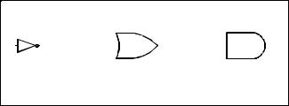
A natural way to describe discrete components is to use a data flow model. Discrete gates such as a one input and one output NOT gate, INV1, two inputs and one output AND gate, AND2, and two inputs and one output OR gate, OR2, can be modeled fairly easily, and they are illustrated in Figure 2-1. The logic gates in Figure 2-1 have their inputs and outputs labeled. These components will be used to illustrate more examples of elaborate logic devices, such as a digital memory element.
Example of Discrete Components
n nx |
x |
|
|
|
z |
x |
|
|
|
z |
|
|
|||||||||
y |
|
|
|
y |
|
|
|
|||
INV1 Gate |
|
|
|
|
|
|
|
|
||
|
OR2 Gate |
|
AND2 Gate |
|
||||||
Figure 2-1. Example of Discrete Components
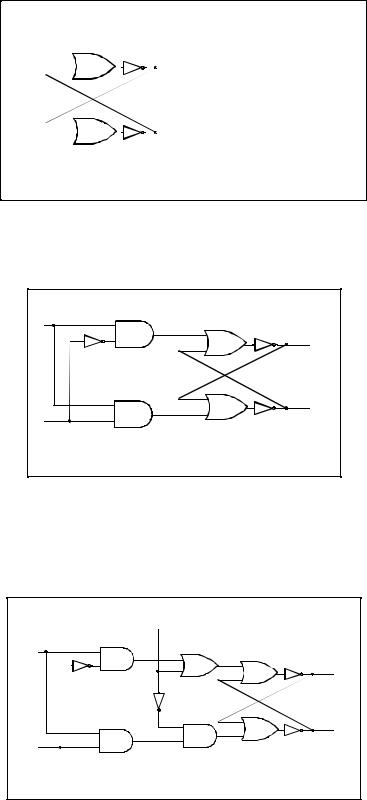
There are many types of memory elements that one can create using the basic gates shown in Figure 2-1. A simple memory block that one can make is an RS flip flop which uses two OR2 and INV1 gates. For the sake of consistency with the previous example, NOR2 is not included for now. Even though OR2 is used to create an RS flip flop, DeMorgan’s law would also permit AND2 to be used as well.
Notice the flip flop is named RS because the flip and flop can be set (output=1) or reset (output=0) depending on the inputs (R and S). When both R and S inputs are set to zero, outputs (q and nq) will be suspended to the previous values of R and S. Be aware that both R and S, at the same time, can’t be set to one for two reasons. The first reason is that once R and S become one, output q and nq will no longer be complementary to each other. Both q and nq will become zero, and this violates the assumption of complementing flip flop output. Second, once the output q and nq become zero, the next state after R and S change, outputs q and nq are impossible to predict due to the feedback of q and nq values. See Figure 2- 2 for the RS flip flop logic truth table.
Although an RS flip flop is easy to implement, it is not an ideal memory device due to its incomplete input states. From the perspective of a digital designer, it is cumbersome to guarantee the partial input state. A better way to use the same memory block is to modify the RS flip flop to take care of the partial input problem. One simple solution is to add two AND2 gates at the front of RS flip flop to prevent R and S from becoming one at the same time. The resulting circuitry is called a D latch. See Figure 2-3 for this modified memory element..
13 |
Copyright 1996, CERL / EE, V1.00 |
Digital Design VHDL Laboratory
2.VHDL Behavior and Structure models
pepe, 5/23/96
|
|
RS Flip Flop |
|
|
|
|
||||||
|
|
|
|
|
|
|
|
|
|
|
|
(next) |
|
|
o1 |
R S |
q -> q |
||||||||
R |
|
|
|
|
n2 |
0 0 |
0 |
0 |
||||
|
|
|
|
|||||||||
|
|
|
|
|
|
|
|
q |
0 0 |
1 |
1 |
|
|
|
|
|
|
|
|
||||||
|
|
|
|
|
|
|
|
|
0 |
1 |
0 |
1 |
|
|
|
|
|
|
|
|
|
0 |
1 |
1 |
1 |
|
|
|
|
|
|
|
|
|
1 |
0 |
0 |
0 |
S |
|
|
|
|
|
|
|
nq |
1 |
0 |
1 |
0 |
|
|
|
|
|
|
|
1 |
1 |
0 |
x |
||
|
|
|
|
|
||||||||
|
|
|
|
|
n3 |
|||||||
|
|
|
o2 |
1 |
1 |
1 |
x |
|||||
|
|
|
|
|
|
|
|
|
||||
Figure 2-2. RS Flip-flop
A D latch functions very similar to an RS flip flop because it remembers past states. However, it works differently because output is triggered by the level of the input signal instead of the input signal edge. As a matter of fact, a flip flop works differently from a latch because the flip flop output signal is triggered at the clock edge and the latch output signal is triggered at the level of clock signal.
|
|
D Latch |
c |
|
o1 |
|
|
n2 |
n1 |
a1 |
q |
|
||
d |
|
n_q |
|
n3 |
|
|
a2 |
o2 |
|
|
Figure 2-3. D Latch
Digital circuitry during the beginning of operation, especially memory elements, will go to erroneous states unless provision is made for startup operation. At the initial stage of the memory operation, the value stored inside of the memory element is unknown, and, if this unknown is to be applied to rest of the system, the system will almost be guaranteed to produce error. The modification to D latch is shown in Figure 2-4. The new latch get reset circuitry so the internal value stored can be set to zero (low) whenever the reset signal goes high.
|
D Latch with Reset Control |
|
|
reset |
|
|
|
c |
|
o3 |
o1 |
|
|
||
|
|
|
n2 |
n1 |
a1 |
|
q |
|
|
||
|
|
n3 |
|
|
|
|
n_q |
d |
|
|
n3 |
a2 |
a3 |
o2 |
|
|
|
||
|
|
|
|
Figure 2-4. D Latch with Reset Control
although the difference between flip flops and latches have been discussed, it is important to note the application side of these memory elements. In the world of digital design, the majority of digital system is
14 |
Copyright 1996, CERL / EE, V1.00 |
Digital Design VHDL Laboratory
2.VHDL Behavior and Structure models
pepe, 5/23/96
running synchronously with the system clock. Since flip flops activate at an instance in time to acquire data, relatively speaking, flip flops are more useful than latches because the output of flip flops is held constant for a full clock cycle instead of half a clock cycle.
Cascading two D latches can produce a D flip flop. The clock signal that runs through these two latches is inverted so data can pass through the latches in pipeline fashion. Due to the holding of input data at the lower phase clock signal, input signal of the first latch is preserved for the instance when the clock signal goes down. Simultaneously, the signal output from the first latch is acquired by the second latch, and the signal is held constant until the second latch’s clock goes down. A D flip flop drawing made by cascading two D latches is shown below in Figure 2-5.
D Flip Flip
reset
d
|
reset |
|
|
reset |
d |
q |
|
d |
q |
|
||||
c |
nq |
|
c |
nq |
D Latch |
D Latch |
c
Figure 2-5. D Flip-flop
Now the memory basics have been explained, and it is time to model some of the memory block using VHDL. The difference between structure, dataflow, and behavior models will be shown in later examples. For example, in Listing 2-1, each discrete logic component, AND2, OR2 and INV1, is defined at the beginning using the dataflow model as state before. Notice that VHDL programming structure is declared with entity statement first and followed by an architecture statement. Signals defined in the entity block under the keyword port are visible inside of the architecture block.
-- INV1 Gate |
|
-- |
|
entity inv1 is |
|
port( |
x: in bit; |
|
nx: out bit); |
end inv1; |
|
architecture behav of inv1 is begin
nx <= not x; end behav;
--AND2 Gate |
|
-- |
|
entity and2 is |
|
port( |
x, y: in bit; |
|
z: out bit); |
end and2; |
|
architecture behav of and2 is begin
z <= x and y; end behav;
-- OR2 Gate |
|
-- |
|
entity or2 is |
|
port( |
x, y: in bit; |
|
z: out bit); |
end or2; |
|
15 |
Copyright 1996, CERL / EE, V1.00 |
Digital Design VHDL Laboratory
2.VHDL Behavior and Structure models
pepe, 5/23/96
architecture behav of or2 is begin
z <= x or y; end behav;
Listing 2-1. Dataflow Modeling of AND2, OR2 and INV1 Gates
As its name implies, structures modeling uses the gates defined above to connect to others to make into a system. The process of describing the system structure in gate connection is shown in Listing 2-2. The VHDL code after the gate definitions shown in Listing 2-1 shows how to connect gates, and this is done through the use of VHDL statement map.
--
-- structure modeling of D latch
--
entity lat_ds1 is
port( c, d: in bit; -- input data q, nq: inout bit);
end lat_ds1;
architecture struct of lat_ds1 is
signal i1_nx: bit; signal i2_nx: bit; signal i3_nx: bit; signal a1_z: bit; signal a2_z: bit; signal o1_z: bit; signal o2_z: bit;
component and2
port(x, y: in bit; z: out bit); end component;
component or2
port(x, y: in bit; z: out bit); end component;
component inv1
port(x: in bit; nx: out bit); end component;
begin
-- structure connection
a1: and2 port map(c, i1_nx, a1_z); a2: and2 port map(c, d, a2_z); o1: or2 port map(a1_z, nq, o1_z); o2: or2 port map(a2_z, q, o2_z); i1: inv1 port map(d, i1_nx);
i2: inv1 port map(o1_z, q); i3: inv1 port map(o2_z, nq);
end struct;
Listing 2-2. D Latch Structure Modeling
The variables inside of the mapping statements are declared after the D latch architecture declaration, architecture struct of lat_ds1 is, and before the begin statement. These signals can only be used here, and they are not accessible by other architecture code blocks.
16 |
Copyright 1996, CERL / EE, V1.00 |
Digital Design VHDL Laboratory
2.VHDL Behavior and Structure models
pepe, 5/23/96
Gate components used here are also required to be declared. The declaration of a component is similar to C, FORTRAN or Pascal programming where all procedures or subroutines are required to be declared before use. However, it is not exactly the same as doing programming because each component declared could be physical part rather than a conceptual abstract. For example, the ports declared by component do have corresponding physical meaning, namely wires to carry signals. This concept should be understood from the digital hardware engineer perspective.
Now, consider taking the same D latch circuit and describing or modeling it behaviorally in VHDL. This code is shown in Listing 2-3. As we have noticed, the VHDL code here is shorter than its corresponding structure model because the circuit behavior is directly described. It is a higher level modeling, and it can be done easily if the designer knows exactly how his circuit behaves. Many times, the digital circuit designer knows how the circuit should behave but is not sure if the actual circuit behaves as he predicts. Therefore, it is useful to construct the circuit as a structure model and verifies its working order. Behavior modeling saves time and it is based on the assumption that the designer knows his circuit’s behavior well. If the assumption about the circuit is wrong, then behavior modeling can lead to a disastrous result. Remember, behavior modeling should be used as much as possible when modeling digital circuits because it will save much development time.
In the field of VLSI design, the translation of a behavior model to a structure model is called hardware synthesis, and it relies much on the software intelligence. During the process of mapping a VHDL circuit to the actual hardware, it is best to specify as much structure as possible if the speed and the size requirement of the circuit are a concern. As an analogy, think of a programmer who wants his code to be as fast and efficient as possible. The programmr does better write the code in assembly (or even better - machine language) instead of relying on a the high level language compiler. For the exercises here, problems mainly focus on translating VHDL code to hardware. In other words, VHDL will be used as a programming language to map into hardware. Again, remember the concept of hardware synthesis. In hardware synthesis, the digital designer needs to be conscious of the final form of the mapped circuit.
--
-- behavior modeling of D latch
--
entity lat_db1 is
port( c, d: in bit; -- input data q, nq: inout bit
);
end lat_db1;
architecture behavior of lat_db1 is
begin
-- behavior model
behavior: process (c) begin
if c='1' then
q |
<= d; |
nq |
<= not d; |
end if; |
|
end process behavior;
end behavior;
Listing 2-3. D Latch Behavior Modeling
17 |
Copyright 1996, CERL / EE, V1.00 |