

12.Phase Lock Loops
.pdfPLL DESIGN EQUATIONS |
267 |
Using Eq. (12.52) to replace Rs above,
Cωn2 |
D 2Cωn |
2ωn |
|
Cωn2 |
|
|
|
||
|
KtFdc |
1 |
|
KtFdc |
|
FdcKt |
|
Rp |
12.54 |
|
|
|
|
|
|
|
|
||
If, in addition to the damping ratio and the natural frequency, values for C and the dc gain are chosen, then the required resistance values can be found as summarized below. Solution of Eq. (12.54) gives the value for Rp.
|
D KpdKvcoC |
|
|
|
|
ωn |
C |
|
|
Nωn2 |
Fdc |
|||||||||||
Rp |
|
|
|
1 |
|
|
|
|
|
2 KpdKvco |
|
|
|
KpdKvcoFdc |
|
N |
||||||
D KtC |
ωn |
|
|
C |
|
Nωn2 Fdc |
|
|
||||||||||||||
|
|
|
|
|
|
|||||||||||||||||
|
|
1 |
|
|
2 Kt |
|
|
|
|
KtFdc |
|
|
|
1 |
|
12.55 |
||||||
Rs D |
KpdKvcoFdc |
Rp |
|
|
|
|
|
|||||||||||||||
|
|
|
|
|
|
|
||||||||||||||||
|
NCωn2 |
|
|
|
|
|
|
|
|
|
||||||||||||
|
|
|
KtFdc |
|
|
|
|
|
|
|
|
|
|
|
|
12.56 |
||||||
|
D |
|
|
Rp |
|
|
|
|
|
|
|
|
||||||||||
|
Cωn2 |
|
|
|
|
|
|
|
|
|||||||||||||
Rin D |
Rp |
|
|
|
|
|
|
|
|
|
|
|
|
12.57 |
||||||||
Fdc |
|
|
|
|
|
|
|
|
|
|
|
|
|
|||||||||
The type 2 PLL equations are found by allowing Rp ! 1.
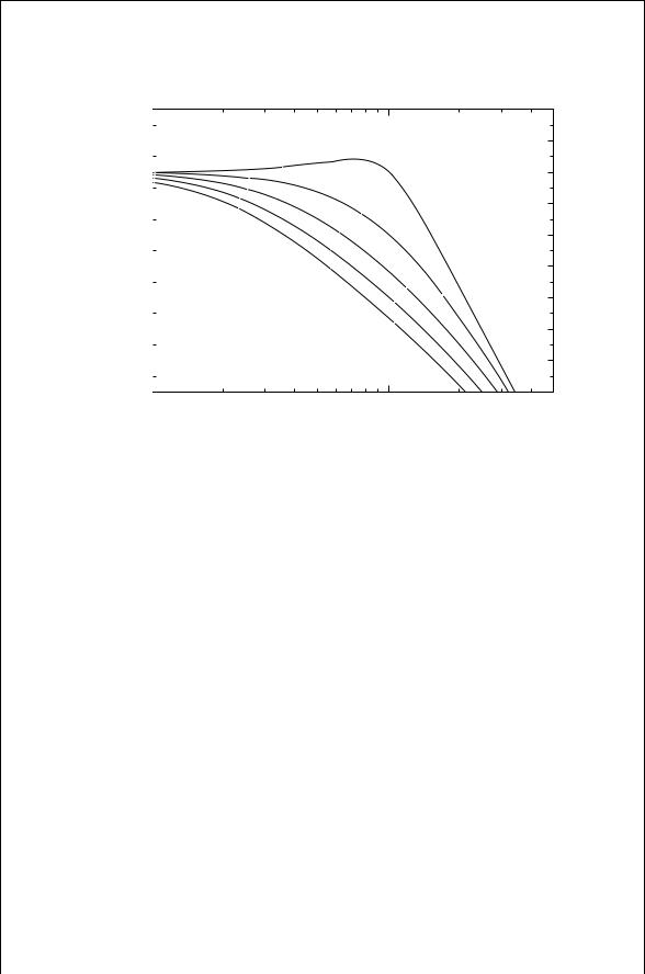
Figure 12.13 illustrates the expected PLL bandwidth verses frequency for several values of damping ratio. These results are calculated for a second-order loop with a natural frequency of 1 Hz. The results can be easily scaled for loops requiring higher natural frequencies. When < 1, the PLL is under damped and peaking occurs. The response of such a loop to a disturbance will be a damped oscillation that finally converges to the final answer. When > 1, the PLL is overdamped. The 3 dB gain frequency for a damping of 1.0 is 2.4 Hz. If a 3 dB frequency of 50 kHz were required with a damping of 1.0, then a natural frequency of 20.833 kHz would be chosen. The requirements of the PLL design and the available parts will determine the best choice for the natural frequency and damping ratio.
A second-order loop can be built either as type 1 or type 2 with either an inverting or noninverting loop filter. The actual loop order may be several orders higher than 2 when all the extraneous poles are considered. A good design procedure initially ignores these poles and assumes ideal VCOs, phase detectors, op-amps, and so on, with which it determines a set of loop filter values based on the second-order model. Subsequently nonideal parts can then be added to the model and the analysis refined as more values become available. Computer modeling is encouraged for this process.
268 PHASE LOCK LOOPS
|
6.0 |
|
|
|
|
|
|
|
|
|
3.0 |
|
|
|
|
|
|
|
|
|
0.0 |
|
|
|
|
|
|
|
|
dB |
–3.0 |
|
|
|
|
|
|
||
|
|
|
|
|
Gain, |
–6.0 |
|
|
|
|
|
|
|
|
Loop |
–9.0 |
|
|
|
|
|
|
||
–12.0 |
|
|
|
|
|
|
|
|
|
|
|
|
|
|
|
–15.0 |
|
|
|
|
|
|
|
|
|
–18.0 |
|
|
|
|
|
|
|
|
|
–21.0 |
|
|
|
|
|
|||
|
0.1 |
|||
FIGURE 12.13 ratios.
Damping Ratio |
0.5 |
1.0
1.5
2.0
2.5
1.0 Frequency, Hz
PLL response with natural frequency of 1 Hz and various damping
12.11.2Noninverting Loop Filter
Design equations can be developed for a noninverting loop filter like that shown in Fig. 12.5. The filter transfer function is
F s |
D |
1 |
C |
Rpjj[Rs C 1/sC ] |
|
|
|
Rin |
|
||||||
|
|
|
|
||||
|
D |
|
1 C Rp/Rin C sC[ RpRs/Rin C Rp C Rs] |
12.58 |
|||
|
|
|
|||||
|
|
|
|
1 C sC Rp C Rs |
|
||
The closed loop gain is found by substituting Eq. (12.58) into Eq. (12.37) while making use of Eq. (12.50):
H s |
D |
NKtf1 C Rp/Rs C sC[ RpRs/Rin C Rp C Rs]g |
|
12.59 |
|
s[1 C sC Rp C Rs ] C f1 C Rp/Rin |
|||||
|
|
||||
|
|
C sC[1 C RpRs/Rin C Rp C Rs]gKt |
|
||
|
D |
[NKt/C Rp C Rs ]f1 C Rp/Rs C sC[ RpRs/Rin C Rp C Rs]g |
12.60 |
||
|
s2 C sf[1/C Rp C Rs ] C [RpRsKt/ Rp C Rs Rin] |
||||
|
|
||||
C Ktg C [ Rin C Rp/ Rp C Rs ]Kt/C

PLL DESIGN EQUATIONS |
269 |
From this the loop natural frequency and damping ratio can be identified:
ωn D |
|
|
Rpin CRs |
pRinCt |
|
12.61 |
||
|
|
|
|
|
R R |
K |
|
|
|
|
|
|
|
C |
|
|
|
|
D |
|
Rin C CRpRsKt C Rin Rp C Rs CKt |
12.62 |
||||
|
|
|||||||
|
|
|
|
2ωnC Rp C Rs Rin |
|
|||
The typical synthesis procedure is to design a PLL with a given natural frequency and damping ratio using a specified capacitance, C. Solving Eq. (12.61) for Rp C Rs and substituting this into Eq. (12.62) gives an equation in terms of one unknown, Rp. First, from Eq. (12.61),
|
|
|
|
R |
|
|
Kt Rp C Rin |
|
|
R |
|
|
|
12.63 |
|||||
|
|
|
|
|
|
|
|
|
|
|
|||||||||
|
|
|
|
|
s |
D |
RinCωn2 |
|
p |
|
|
||||||||
then substitution gives |
|
|
|
|
|
|
|
|
|
|
|
|
|
|
|
|
|||
|
Kt Rp C Rin |
|
|
1 |
|
|
|
Rin |
|
CRpKt |
|
Kt Rin C Rs |
|
Rp |
|||||
|
RinCωn2 |
D 2 ωnCRin |
C |
RinCωn2 |
|
||||||||||||||
|
|
|
|
|
|
|
|||||||||||||
|
|
|
C |
CKtRin |
Kt Rin C Rp |
|
|
|
|
|
|
12.64 |
|||||||
|
|
|
RinCωn2 |
|
|
|
|
|
|||||||||||
|
|
|
|
|
|
|
|
|
|
|
|
|
|
||||||
This has one unknown, Rp, that can be solved by the quadratic formula as follows:
0 D Rp2 Kt2 CKtRinωn2 C Rp2KtRin Kt ωn |
|
C Rin2 ωn2 C Kt2 2 Ktωn |
12.65 |
So, if |
|
a D Kt2 CKtRinωn2 |
12.66 |
b D 2KtRin Kt ωn |
12.67 |
c D Rin2 ωn2 C Kt2 2 Ktωn |
12.68 |
then |
p |
b C b2 4ac
Rp D 12.69 2a
Again, the value of Rin is associated with the voltage gain of the noninverting loop filter:
Rp |
12.70 |
Rin D Fdc 1 |
The value for Rs is obtained from Eq. (12.63).

270 PHASE LOCK LOOPS
The type 2 PLL parameters with the noninverting loop filter can be found by letting Rp ! 1. Thus the design equations for a given natural frequency, damping ratio, and capacitance are
|
ωn2 |
D |
|
|
Kt |
|
|
|||
|
RinC |
|
|
|
||||||
or |
|
|
|
|
|
|
Kt |
|
|
|
|
Rin D |
|
|
|
||||||
|
Cωn2 |
|
|
|
||||||
and the damping ratio is |
|
|
|
|
|
|
|
|
|
|
2ωn D 0 C |
RsKt |
C Kt |
||||||||
|
||||||||||
Rin |
||||||||||
or |
|
|
|
2ωn Kt |
|
|||||
R |
s D |
R |
|
|
||||||
|
|
|||||||||
|
|
in Kt |
|
|
||||||
The value for Kt is given by Eq. (12.50).
12.71
12.72
12.73
12.74
12.12PLL OSCILLATORS
A phase lock loop will have a least two oscillators associated with it: the reference oscillator and the voltage controlled oscillator. The reference is typically a fixed frequency, but in some applications it may change over a wide frequency range. In any event, the VCO must be able to follow it.
The types of oscillators used depend on the design requirements and the frequency range. Low-frequency oscillators use a resistor capacitor combination to set the frequency. A larger charging current in the capacitor results in a higher-oscillation frequency. These oscillators can be used from a few hertz to several megahertz. They can sweep a wide frequency range, but the output is usually noisy and drifts rapidly with temperature. This oscillator is frequently found in simple PLL ICs.
An LC oscillator’s frequency is set by a combination of inductors and capacitors in a resonant circuit. This oscillator is useful from about 100 kHz to somewhat above 5 GHz. A high Q network will produce a very clean output with a small tuning range. Frequency control of a voltage-controlled version can be built either by varying a dc voltage in the circuit or, more commonly, by adding a voltage-controlled capacitor, called a varactor diode, to the resonant network. A varactor is a low-loss reverse-biased diode whose depletion capacitance has been optimized for large change with changes in bias. Reverse-biased voltages range from about 2 volts to 28 volts. Capacitance values range from fractions of a pF to 500 pF.

PHASE DETECTOR TYPES |
271 |
Oscillator design at any frequency is a specialized area. The design or purchase of either the reference oscillator or the VCO is an activity that should be completed before the PLL design is attempted. Available power supply voltages will determine the tuning voltage available for the VCO. Simulations can determine an approximate tuning rate for the VCO, from which an appropriate oscillator type can be picked from the various available types and manufacturer’s data sheets. The characteristics of both oscillators should be well defined.
12.13PHASE DETECTOR TYPES
Previous sections have introduced both the mixer and flip-flop-based phase detectors. These are the two main configurations that are widely used, although there are many specialized variations of each type. A sampling phase detector is a third type that is frequently used in RF and microwave applications. A careful study of the design requirements will usually point to the correct choice.
12.13.1Mixer Phase Detectors
Mixers with a dc coupled output make an excellent phase detector. At high frequencies, a mixer may be either active (with transistors) or passive (with diodes). The diode versions provide better dc stability and are generally preferred. The diode mixer is the best choice for low-noise designs or when the PLL reference input is a low-level signal buried in noise. When the PLL is locked and running closed loop, both frequencies will be exactly the same. The two inputs are applied to the RF and local oscillator (LO) ports of the mixer, and the beat note output comes from the intermediate frequency (IF) port. The IF port is loaded with a total resistance of 50 to 1000 ". Blocking capacitors are used to ac couple the signals into the two input ports, but the IF output port must not be ac coupled. A mixer must be chosen that is appropriate for the frequency range and power level of the inputs. The beat note output is typically 100 mV to 1 volt peak to peak, depending on the mixer type and application. The mixer type phase detector is the best choice when the input signal is pulsed or noncontinuous. The ability of this type of detector to resolve an angular difference is limited to š90°. It has no ability to determine which input is the higher frequency. Thus it is not capable of frequency discrimination.
12.13.2Sampling Phase Detectors
Sampling phase detectors (SPD) can be used in a phase lock loop to produce an output frequency that is an integer multiple of the reference frequency. This mixer relies on a device to generate a comb of frequencies at multiples of the reference. The VCO then mixes with the correct spectral line to produce an error signal. A SPD is used in a phase lock loop where the output frequency is an integer multiple of the input frequency. If fout D N Ð fin C f, the SPD output

272 PHASE LOCK LOOPS
is a cosine wave of frequency f. If fout is exactly N times fin, the SPD output is a dc level proportional to the phase difference between its two inputs. The input frequency, fin, is typically between 50 and 200 MHz at a power level of C20 dBm or higher, and fout can be at any harmonic of fin up to 18 GHz. The low-frequency high-power input signal produces a comb of spectral lines inside the SPD where lines up to the 150th multiple are useful.
A sampling phase detector is one of the best choices for a very high frequency PLL where excellent phase noise is a requirement. However, an external circuit is usually required to bring the VCO into lock range. Additionally provisions must be made to ensure that the VCO will be locked to the correct multiple of fin.
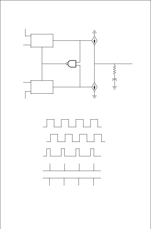
12.13.3Flip-Flop Phase Detector with Frequency Acquisition Aiding
All of the other phase detectors previously discussed have a major drawback. They produce an output equal to the difference between the two input frequencies, either a cosine wave or a triangle wave. However, this output does not have information about whether the VCO is too high in frequency or too low. A PLL using these phase detectors must also include a sweep or search circuit to initially bring the VCO close enough to lock. This can involve a substantial amount of circuitry. The phase detector circuit shown in Fig. 12.14a uses positive edge triggered D type flip-flops to overcome this problem. The D inputs are connected to a logic 1. Figure 12.14b illustrates the timing sequence. The signal, f1 positive edge arrives first causing Q1 to clock high. Later positive edge of f2 causes Q2 to clock high. Two 1’s at the NAND gate’s input cause its output to go low and clear both Q1 and Q2. The output at Q2 is a pulse whose duty cycle represents the time delay between f1 and f2. The pulse at Q2 is very short, being the sum of the propagation times through the flip-flops and gates. Of course, if f2 arrives before f1, then the output pictures are reversed.
The outputs, Q1 and Q2, turn on the current sources. These current sources either source or sink current to the capacitor which ramps up or down the phase detector output voltage. The action of this circuit is identical to the op-amp integrator. So the phase detector has added another integrator to the PLL. A PLL using this circuit will be at least a type 2 loop.
The advantage to this circuit is the self-searching capability. If f1 is higher than f2, the output voltage will go to the positive voltage limit. If f1 is lower than f2, the output voltage will go to the negative voltage limit. If f1 equals f2, the output voltage will be proportional to the phase difference. Thus this circuit can sense which input frequency is higher. The output voltage can then be used to drive the VCO in the correct direction to bring the loop into lock. Once the two frequencies are the same, this circuit becomes a phase detector and drives the VCO for no phase error.
This phase detector circuit is used in many present-day frequency synthesizer ICs, where its built-in search capability makes it ideal for a variety of applications. However, there are at least two drawbacks to this circuit that force limits on its usage. The largest problem is the short pulse on one of the flip-flop
PHASE DETECTOR TYPES |
273 |
High |
Current Source |
|
D
Q 1
D
Flip-Flop
f 1
Ck
Phase Detector
Clear
R
Ck |
C |
f 2
D
Flip-Flop
Q 2
D
High |
Current Sink |
(a )
f 1
f 2
Q 1
Q 2
Clear
(b )
FIGURE 12.14 (a) Phase detector using a D flip-flop and (b) the timing chart.
274 PHASE LOCK LOOPS
outputs. With high-speed logic, this pulse is only a few nanoseconds long. If f1 and f2 are high in frequency, this may be a significant part of their period. This pulse dead time due to propagation delays results in a nonlinear phase detector transfer curve. In older versions there were flat spots with zero gain and regions where the gain reversed its slope. The pulse also contributes heavily to the output noise, and it can easily add 20 dB of noise to the PLL output even in the most modern devices. The second problem is that the searching
capability |
can become confused |
if there is any interruption in |
either |
f1 or |
f2. This |
circuit should be used |
in applications where very low |
phase |
noise |
is not required and the inputs are continuous. For this phase detector the gain is
Kpd D 1/4 .
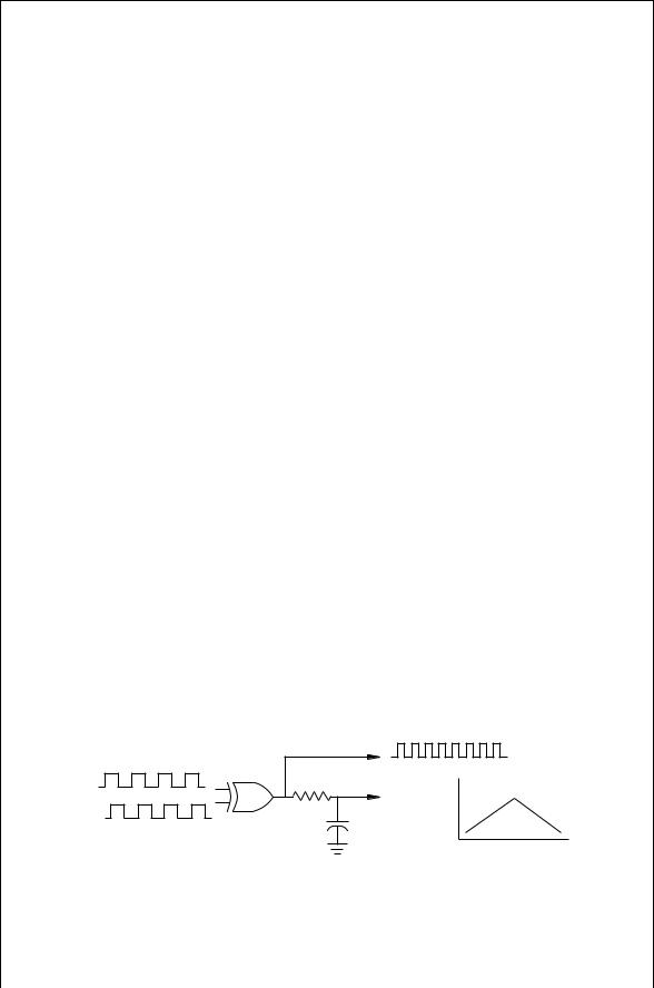
12.13.4Exclusive OR Phase Detector
An exclusive OR gate works as a frequency doubler and phase detector. Figure 12.15 illustrates a typical connection for the phase detector. For correct operation, both inputs f1 and f2 must be at the same frequency, and both must have 50% duty cycles. The XOR output will be a logic level waveform at twice the input frequency. The duty cycle of the output depends on the phase difference between the two inputs. Phase shifts of 90° or 270° produce a 50% output. The RC low-pass filter produces a dc value proportional to the duty cycle. For a 90° or a 270° phase difference, the filter output is one-half the difference between the logic highand logic low-output voltages.
The XOR gate is the functional equivalent of the balanced mixer. This circuit is useful for PLL applications requiring a high-frequency VCO to be divided down and locked to a low-frequency logic level frequency reference. This phase detector is suitable for low-phase noise applications, but it frequently requires an external search circuit to initially achieve lock. The gain, Kpd, of this phase detector is 1/ volts/rad.
Doubled
Frequency
Output
f 1 |
R |
Phase |
|
|
Detector |
f 2 |
|
Output |
|
|
C |
0 |
360 |
|
Phase Difference |
FIGURE 12.15 Exclusive OR phase detector.
DESIGN EXAMPLES |
275 |
12.14DESIGN EXAMPLES
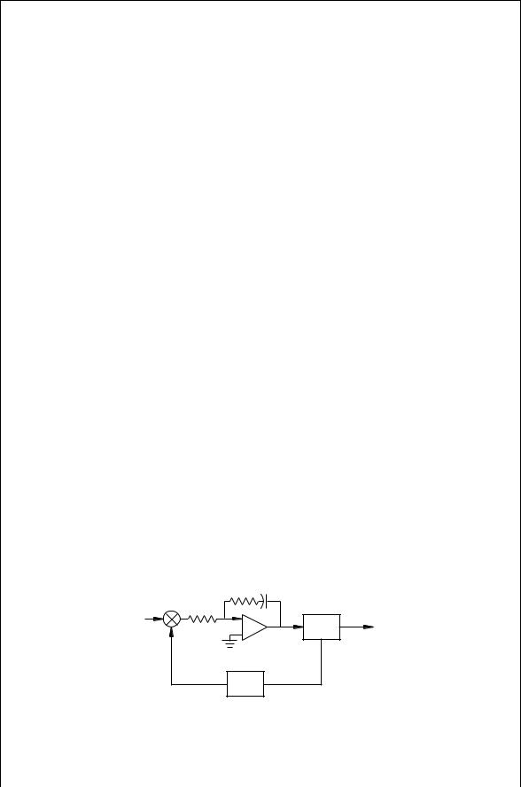
Example 1. The phase lock loop design shown in Fig. 12.16 requires an output frequency of 1600 MHz and the reference oscillator is 100 MHz. The design approach chosen is to use an inverting type-2 loop filter with a frequency divider and a mixer phase detector. The VCO chosen shows a typical tuning slope of 1 MHz/volt. Measurements of the phase detector output show a cosine wave that is 100 mV peak to peak. A 3 dB bandwidth of 100 kHz is required with a damping ratio of 1.
a.Using a 100 pF capacitor, find the remaining loop filter values.
b.Using a 10 k" Rin, find the remaining loop filter values.
Solution 1. From the graph in Fig. 12.13, the 3 dB frequency for a damping ratio of 1 is at 2.45 Hz. The type 2 circuit for this example is shown in Fig. 12.16. If 100 kHz 3 dB frequency is required, the natural frequency is found from scaling the graph. Thus fn D 100 kHz/2.45 D 41 kHz. The output frequency is 16 times the input frequency, so N D 16. The value for Kvco is specified at 1 MHz/volt. The phase detector output is a cosine wave. If the loop locks at 90° or 270°, the phase detector output voltage is zero. For a positive Rin, the slope is the first derivative evaluated at 270°, so Kpd D 50 mV/rad.
For part a, use the equations derived earlier with C set at 100 pF. Then Kt D [ 1 Ð 50 /16] Ð 2 Ð 103, and from Eq. (12.48), Rin D 2.96 k". Finally Eq. (12.49)
gives Rs D 77.6 k".
For part b, Rin D 10 k". With Rin set, C D 29.6 pF and Rs D 262.4 k".
Example 2. The synthesizer design shown in Fig. 12.17 requires an output frequency from 900 to 920 MHz. The output frequency can be changed in 1 kHz steps by changing the divide ratio. Design a PLL using a synthesizer IC and an external VCO. The synthesizer IC data sheet lists the current mode phase detector output as 5 mA/rad. The VCO data sheet lists the tuning rate at 10 MHz/volt.
Solution 2. The output frequency must be an integer multiple of the reference frequency, so the reference frequency is 1 kHz. The circuit diagram is shown
Phase |
R s |
C |
|
Detector |
R in |
|
|
f ref = 100 MHz |
|
|
|
– |
VCO |
f out = 1600 MHz |
|
|
+ |
||
|
16 |
|
|
FIGURE 12.16 PLL for Example 1.
276 PHASE LOCK LOOPS
|
Synthesizer |
|
IC |
f ref = 1 kHz |
VCO |
|
R s |
|
C |
|
Divide by |
|
N Control |
f out
900 –920 MHz
FIGURE 12.17 Synthesizer design for Example 2.
in Fig. 12.17. The divide ratio must change from 900 MHz/1 kHz or 9 Ð 105 to 920 MHz/1 kHz or 9.2 Ð 105. The midpoint value, 9.1 Ð 105, can be used for the design. A damping ratio of 1 is chosen for a rapid settling time when the divide ratio changes. The loop filter must attenuate the pulses from the phase detector output running at 1 kHz. Figure 12.13 shows that 14 dB of attenuation can be expected at 10 times the natural frequency. With a slope of 20 dB/decade, 34 dB attenuation can be expected at 100 times the natural frequency. Choosing fn D 10 Hz will work with a 1 kHz reference frequency. Here the value of Kt is in dimensions of V/A:
Kt D |
KvcoKpd |
Ð |
MHz |
Ð |
mA |
Ð |
2 rad |
N |
volt |
Hz |
Hz |
Evaluation of this gives Kt D 0.345 A/V. To find Rs and C, Kt must be multiplied by Rin. This will cancel the Rin in Eqs. (12.46) and (12.47). Thus from the design equations Rs D 364 " and C D 87.45 F.
Example 3. A frequency synthesizer contains a phase lock loop circuit. Inspection shows that the loop filter is to be a type 1 noninverting configuration. The data sheets for the phase detector show that the output waveform has a slope of 100 mV/rad. The VCO nominal output frequency is 3 GHz with a tuning rate of 100 MHz/volt. The reference is a 100 MHz crystal oscillator. If Rin D 620 ", Rs D 150 ", Rp D 56 k", and C D 1 nF, what is the expected 3 dB bandwidth and damping ratio for this PLL?
Solution 3. With a 3 GHz output and a 100 MHz reference, the frequency divide ratio N must be 30. Also Kt D 2.094 Ð 106. Substituting the given circuit values into the analysis equations show that fn D 293.7 kHz and the damping ratioD 0.709. The curve for D 0.709 is not shown in Fig. 12.13, but a value can be found by interpolation. The 3 dB frequency for D 0.5 is 1.8 Hz. The 3 dB frequency for D 1 is 2.45 Hz. A linear approximation for 0.709 is 2.07 Hz. The 3 dB frequency for this PLL is approximately 2.07 Ð fn D 608 kHz.