

12.Phase Lock Loops
.pdfLINEAR ANALYSIS OF THE PLL [1] |
257 |
If the Laplace transform of 1 t is represented by Q s and the Laplace transform
of t |
is represented by Q s , then the Laplace transform of Eq. (12.19) is |
|
|
s Q s C KF s Q s D s Q 1 s |
12.21 |
This linear frequency domain equation for the PLL can be represented as shown in Fig. 12.7.
The solution for the phase error gives
Q s D |
|
|
Q 1 s |
12.22 |
1 |
C |
KF s /s |
||
|
|
|
|
so that the phase shift at the output of the PLL is
Q 2 s D Q 1 s Q s |
|
||||
Q 2 s |
|
G s |
12.23 |
||
|
D P s D |
|
|
|
|
Q 1 s |
1 |
C |
G s |
||
|
|
|
|
||
where G s D VaVbKm/2F s /s. The phase error can in turn be written in terms of this transfer function:
Q s D Q 1 s Q 2 s D [1 P s ] Q 1 s |
12.24 |
If, for example, the phase of the incoming signal is 1 t D ωt C 0 and the PLL has no filter, F s D 1. Readjusting the phase reference as was done in Eqs. (12.16) and (12.17) gives
1 D 1 ω0t
|
|
|
D ω ω0 t C 0 |
||||||
In the frequency domain this becomes |
|
|
|
||||||
|
|
Q 1 |
s |
|
ω ω0 |
0 |
|
||
|
|
|
D |
|
s2 |
C |
s |
|
|
~ |
~ |
|
|
|
|
|
|
|
|
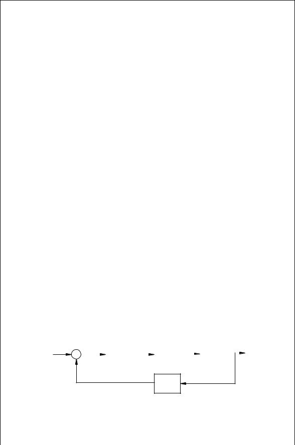
f1(s) |
∆f(s) |
|
|
|
|
|
|
|
|
|
+ |
|
K |
|
|
|
|
|
F (s) |
|
|
|
|
|
|
|
|
||
|
− |
|
|
|
|
|
|
|
|
|
~ |
|
|
|
|
|
|
|
|
|
f2(s) |
|
|
|
|
|
|
|
|
|
|
1/s |
|
|
|
|
|
||
|
|
|
|
|
|
|
|
||
|
|
|
|
|
|
|
|
|
|
12.25
12.26
12.27
FIGURE 12.7 Frequency domain linear phase lock loop.
258 PHASE LOCK LOOPS
The phase error is found from Eq. (12.22):
Q |
D K/s |
s2 |
|
C s |
|
|
s |
1 |
|
ω |
ω0 |
0 |
12.28 |
|
|
|
|
|
||
The inverse transform in this case is straightforward and gives the phase error in the time domain:
t |
D |
ω ω0 |
1 |
|
e Kt |
C |
e Kt |
12.29 |
|||
|
|||||||||||
|
K |
|
|
0 |
|
||||||
The steady state phase error is found by allowing t ! 1: |
|
||||||||||
|
t |
D 1 D |
|
ω ω0 |
|
12.30 |
|||||
|
|
|
|
K |
|
|
|
|
|||
Clearly, the phase will change when the incoming frequency changes, so that phase lock is not achieved.
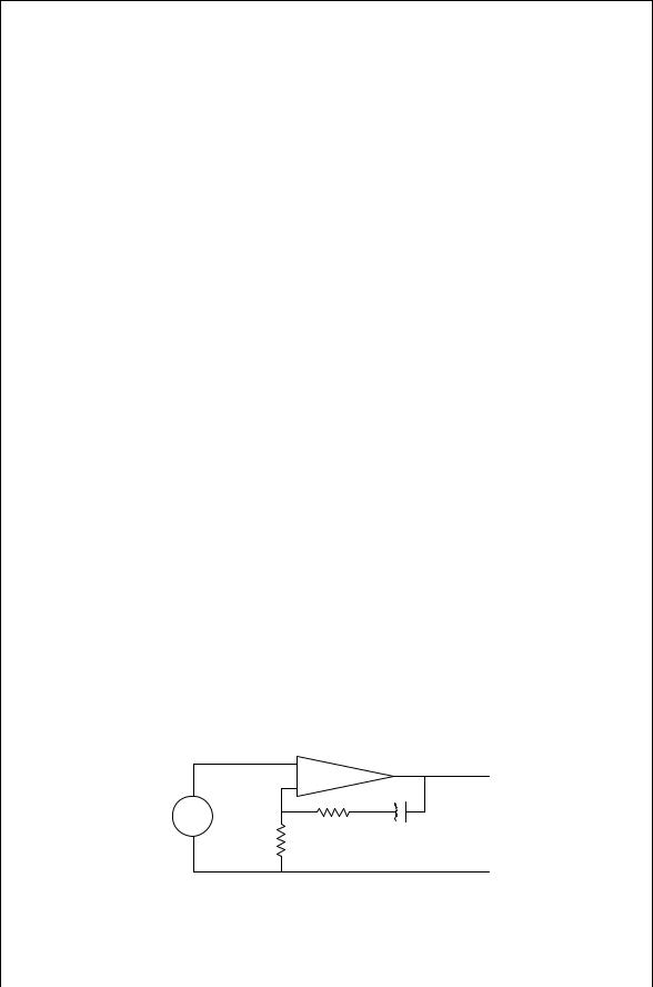
The insertion of a low-pass filter into the PLL will produce lock. An active filter such as that shown in Fig. 12.8 is recognized as basically a noninverting amplifier. The inverting amplifier has right half-plane poles and is therefore unstable. For the noninverting case the voltage gain can be found by writing node equations at the input nodes of the operational amplifier:
|
D |
Vi |
D |
|
C |
R1 |
D |
|
C R1 |
C sCR1 |
|
F s |
|
Vo |
|
1 |
|
R2 C 1/sC |
|
1 |
|
R2 |
1 |
|
|
|
|
|
|
|
|
|
|||
The phase transfer factor is found from Eq. (12.23):
P s |
D |
Q 2 s |
D |
K[ 1 C R2/R1 R1Cs C 1] |
|
Q 1 s |
s2CR1 C CR1K 1 C R2/R1 s C K |
Thus, using Eq. (12.24), the phase error is easily obtained:
Q [1 ]
s D P s 1 s
|
+ |
|
|
− |
|
Vi |
R2 |
C |
|
||
|
R1 |
|
12.31
12.32
12.33
+
V0
−
FIGURE 12.8 Possible active low-pass filter for the PLL.
LOCKING A PHASE LOCK LOOP |
259 |
s |
|
ω ω0 CR1 C 0CR1s |
|
|
12.34 |
||||||||
|
|
|
|
||||||||||
Q |
D s2CR |
1 C |
CR |
K 1 |
C |
R |
/R |
1 |
s |
C |
K |
||
|
|
|
1 |
|
2 |
|
|
|
|
||||
Rather than find the inverse transform this time, the final value theorem may be used to find the steady state phase error:
tlim t |
lim s Q s |
D |
0 |
12.35 |
!1 |
D s 0 |
|
|
|
! |
|
|
|
In this case the phase error is independent of frequency and in the steady state is zero.
12.8LOCKING A PHASE LOCK LOOP
The previous sections examined each of the elements in a PLL. As an example of how these parts go together, consider a simple loop with no frequency divider. Also assume that initially the loop is not locked and that the reference frequency is 100 MHz. A VCO tuning voltage of 5 volts is required to make the VCO frequency be 100 MHz. The phase detector can produce a cosine wave beat note of 1 volt peak to peak.
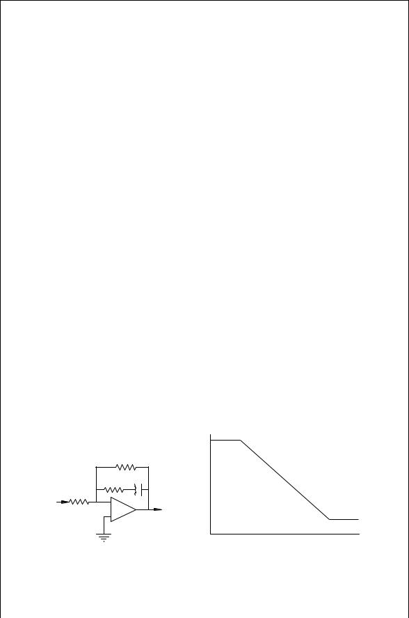
To simplify the design, a type 1 loop filter will be used. This is an inverting op-amp circuit with a gain of 100 at low frequency and a gain of 0.1 at high frequency (Fig. 12.9). With the loop unlocked, the VCO frequency could be anywhere within its operating limits. Assume that it is operating at 101 MHz, so that there is a 1 MHz beat note at the phase detector output when the reference frequency is first applied. This beat note frequency is high enough to only be amplified with a gain of 0.1 by the loop filter. The VCO tuning voltage will be modulated by the phase detector output of 0.1 volt peak to peak, but this voltage will not cause any significant change in the VCO frequency.
With the VCO frequency too far away from the reference frequency, there is not enough gain in the loop to bring the loop into lock. However, if the VCO
|
|
|
+60 |
|
|
Rp |
|
|
|
C |
dB |
|
Rs |
Gain, |
|
Vpd |
Rin |
|
|
|
− |
|
Vtune |
|
+ |
|
−20 |
|
|
|
Beatnote Frequency, kHz
FIGURE 12.9 (a) Type 1 loop filter and (b) its frequency response.
260 PHASE LOCK LOOPS
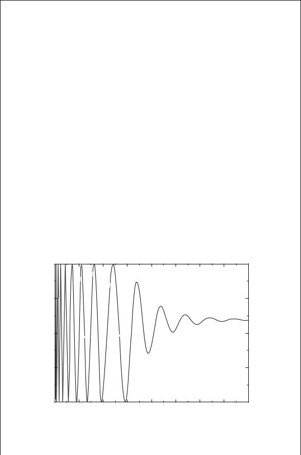
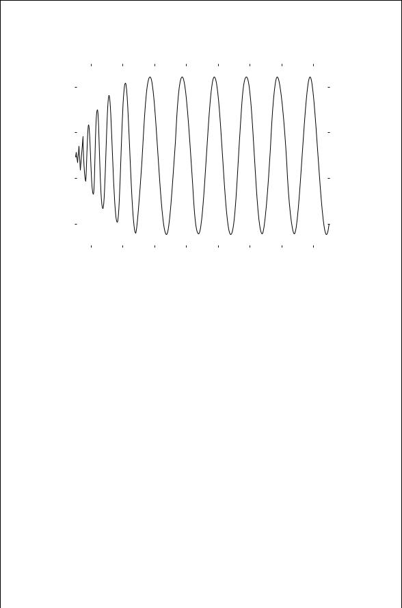
frequency is 100.1 MHz when the reference frequency was applied, the beat note frequency would be 100 kHz. That is well within the high-gain frequency range of the loop filter for this design. The amplified beat note voltage modulates the VCO frequency. As the VCO frequency swings closer to the reference frequency, the beat note frequency gets even lower, it enters an even higher-gain region of the loop filter. This action accelerates the VCO frequency change until it crosses the reference frequency. At this point the beat note frequency is zero. The PLL has been designed as a stable closed loop system, and the VCO is at the same frequency as the reference. The transient phase detector output voltage and the VCO tuning voltage are shown in Figs. 12.10 and 12.11, respectively. The input voltage to the VCO is 5 volts when the PLL is at frequency lock. Since the loop filter has a dc inverting gain of 100, the voltage at the phase detector output is
Ve D |
|
4 |
D 50 mV |
12.36 |
|
100 |
|||
|
|
|
|
The maximum voltage it could reach is 1.0 volt, so from Eq. (12.4) the phase difference is D arccos Ve/0.5 Ð 1.0 D 95.7°. The loop filter will keep the VCO at 100 MHz and maintain a 95.7° phase difference between the two phase detector inputs.
An oscillator accumulates 360° of phase rotation in each cycle. If the frequency increases it will accumulate more phase rotation in a given period of time. If the VCO tries to drift higher in frequency, it will quickly accumulate more phase rotation. The phase detector output voltage will go up, and the loop filter will amplify this change, which will lower the VCO control voltage. The VCO output
FIGURE 12.10 Phase detector voltage as the PLL pulls into lock.
|
|
|
|
|
|
|
LOOP TYPES |
261 |
||
|
|
|
|
|
|
|
|
|
|
|
|
|
|
|
|
|
|
|
|
|
|
|
|
|
|
|
|
|
|
|
|
|
|
|
|
|
|
|
|
|
|
|
|
|
|
|
|
|
|
|
|
|
|
|
|
|
|
|
|
|
|
|
|
|
|
|
|
|
|
|
|
|
|
|
|
|
FIGURE 12.11 VCO tuning voltage as PLL pulls into lock.
frequency will drop and return to 100 MHz. The situation is similar for the VCO trying to move lower in frequency. This is the effect of the negative feedback within the loop. The battle for control goes on continuously. Small changes in the VCO due to temperature, noise, or even gravity cause small frequency changes. The PLL will not tolerate errors due to frequency or phase changes. When an error voltage develops at the phase detector output, the loop filter will amplify it, and the VCO frequency and phase will return to the correct value. The corrective action of the loop will make whatever adjustments are required to hold the phase and frequency constant.
It is important to understand that the initial beat note frequency must be well within the loop filter’s bandwidth to achieve lock without frequency aiding. In any loop the first event is to bring the VCO frequency in line with the reference frequency. Once the circuit is in lock, a steady state phase relationship that satisfies the loop feedback and dc requirements is found and that will hold its lock frequency.
12.9LOOP TYPES
The PLL is a closed loop system controlled by negative feedback. The closed loop gain P(s) is described by
|
G s |
|
H s D |
|
12.37 |
|
||
|
1 C G s /N |
|

262 PHASE LOCK LOOPS
where G s is the open loop or forward gain, and G s /N is called the loop gain. For this discussion, the forward gain G(s) is the product of the phase detector gain, the loop filter gain, and the VCO gain. The frequency divide ratio is N.
The number of pure integrators (or number of poles at the frequency origin) in the denominator of Eq. (12.37) determines the type of the system. This can be produced by an op-amp integrator with near-infinite dc gain. Obviously this cannot be produced with a passive filter where the maximum gain is 1. A VCO is a pure phase integrator that will contribute one pole to the type determination. Therefore a PLL will be at least type 1. A loop filter with a finite dc gain will not increase the type number. A loop filter with an integrator will increase the type to 2.
The order of the PLL is the degree of the denominator polynomial of Eq. (12.37). The loop filter op-amp has at least two significant breakpoints: one at a frequency between 1 and 100 kHz and a second above 10 MHz. The VCO has frequency roll-offs in its modulation performance. A low-pass filter may be included in the phase detector output to further reduce the unwanted high frequencies.
In the previous example using a type 1 loop, the only pure integrator is the VCO, so there is only one pole at dc. The loop filter has a dc inverting gain of 100. If the VCO gain is 1 MHz/volt and the reference frequency is changed to 103 MHz, the VCO tuning voltage will now be 8 volts. With a gain of 100, the phase detector voltage must be Ve D 8/ 100 D 80 mV.
This represents an angular difference of D arccos Ve/0.5 Ð 1.0 D 99.7° in contrast to 95.7° found earlier when the reference frequency was 100 MHz. The phase difference between the VCO and reference frequency was 95.7 degrees. If the reference frequency continues to change, the VCO frequency will change to match it, which in turn will change the phase detector output voltage. As the reference frequency changes in a type 1 loop, the phase difference changes. This is an important characteristic that is sometimes desirable and other times unacceptable.
If the dc gain of the loop filter is increased to 1000, the phase detector output voltage for a 100 MHz lock is only 5 mV. For phase lock at 103 MHz, the phase detector output voltage is 8 mV. These values represent phase differences, , of 90.57° and 90.92°, respectively. If the dc gain is further increased, the change of with frequency will further decrease. If the gain is increased to the limit, the dc feedback resistor, Rp, will approach an open circuit, and the loop filter dc gain will increase to infinity. The loop filter in Fig. 12.5b is transformed to that shown in Fig. 12.5a.
This loop filter is now a pure integrator. The total number of integrators for the PLL with this loop filter is two: one for the VCO and one for the loop filter. This loop filter used in a PLL creates a type-2 loop. Among the features of this loop is the constant phase shift between the VCO and reference frequency that is maintained with a change in frequency.
Type-1 and type-2 loops constitute the majority of applications. Type-3 and higher loops are required to solve frequency change problems in unusual

NEGATIVE FEEDBACK IN A PLL |
263 |
situations. For example, a ground-launched missile must track an orbiting satellite during its own launch and orbital insertion. During the launch phase, the rocket is consuming fuel and thus reducing its mass. With a constant force, its acceleration will be increasing at an increasing rate. As the satellite comes overhead its transmit frequency is shifted due to the relative motion with the rocket. This shift is constantly changing at an increasing rate. Then the booster separates from the rocket, and the force goes to zero during coast. To track the satellite frequency with no phase error requires a PLL type of at least four. Most hightype loops are used to solve complicated motional problems. This discussion will not cover the design details of loops of a type higher than two.
12.10NEGATIVE FEEDBACK IN A PLL
A frequency change that generates a change in the phase of a stable negative feedback loop generates a correction for the phase error. In the previous example the type 1 loop filter was described as having a dc inverting gain of 100. The VCO requires 5 volts to produce a 100 MHz output. An open loop connection of the PLL components will demonstrate what is called the “sense” of the loop. For open loop testing the VCO is connected to a manually adjustable power supply. With the power supply set at 5 volts, there will be a low-frequency beat note observed at the phase detector output. If the voltage is changed to either 4 or 6 volts, the beat note will be 1 MHz. With a mixer as the loop phase detector, the beat note will be a cosine wave at the difference frequency, 1 MHz. The frequency of the VCO cannot be determined from looking at the beat note. The beat note shows the frequency difference between the two signals, but it does not tell which signal is the higher or lower frequency. A complete description of the difference frequency between the VCO and reference requires both a direction and a magnitude. With the loop out of lock, this type of phase detector can only determine magnitude, j j. The VCO frequency must be forced close enough to the reference frequency for the beat note to be inside the loop bandwidth for a PLL with this type of phase detector to pull into phase lock.
In the previous example the VCO frequency increased as the tuning voltage increased. Many VCOs have the opposite characteristic; that is, the frequency decreases with increased tuning voltage. This difference does not change the stability or operation of the closed loop if a mixer is used as the phase detector. If the loop locked up at 90° difference between the two inputs with the positive slope VCO, it will lock up at 270° with the negative slope VCO. The phase detector output in either case will be correct to speed up or slow down the VCO to match the reference input frequency and phase.
Most synthesizer ICs and PLLs using frequency dividers or logic ICs have a different type of phase detector. Using flip-flops to count the input edges, these phase detectors produce an error voltage that has not only a magnitude but also a sense of the direction between the two inputs. The output is a series of voltage or current pulses. The loop filter averages these pulses to form the control voltage
264 PHASE LOCK LOOPS
for the VCO. A pulse duty cycle above 50% indicates that the VCO frequency is higher than the reference frequency, and a duty cycle of less than 50% indicates that the VCO frequency is lower. If the VCO is running faster than the reference frequency, the control voltage will force it toward the correct value. If the VCO is running too low, the error voltage will drive the frequency higher. This type of phase detector can drive a PLL into lock even when the VCO and reference frequencies are a great distance apart, far outside the loop bandwidth. The typical IC synthesizer will have a pin available to reverse the sense of the error voltage to accommodate VCOs of either positive or negative tuning slope.
12.11PLL DESIGN EQUATIONS
A phase lock loop design requires the basic understanding of the locking mechanism as previously discussed. However, the values for the loop filter and other components must be carefully selected to assemble a stable loop. These values can be both analyzed and synthesized using basic closed loop equations and linear algebra.
The normal phase lock loop model includes a phase detector, a loop filter, a VCO and a frequency divider connected as shown in Fig. 12.12. Each block is described by a gain value that may be a constant or a function of frequency. The frequency response of the closed loop is typically displayed as a Bode plot with a minimum frequency of 1 Hz and a maximum frequency between 10 kHz and 10 MHz. This describes the filtering bandwidth and in turn the transient response of the PLL to the input voltage spectrum, Vin.
12.11.1Inverting Loop Filter
The analysis proceeds by writing the voltage equations at points Ve and Vo. Combining these equations produces the well-known equation for closed loop gain of a system with negative feedback. When Kpd is the phase detector gain, F s , is the noninverting loop filter function, and Kvco/s is the VCO gain, the
Vin
|
|
|
|
Phase |
Loop |
|
|
|
|
|
||
|
|
|
|
Detector |
Filter |
|
|
VCO |
|
|
||
+ |
|
|
|
Ve |
|
Vtune |
|
|
Vo |
|||
|
|
Kpd |
F(s) |
Kvco/s |
|
|||||||
|
|
|
|
|
|
|
||||||
|
|
|
|
|
|
|
|
|
||||
– |
|
|
|
|
|
|
||||||
|
|
|
|
|
|
|
|
|
|
|||
N
FIGURE 12.12 Frequency domain closed loop model for a PLL.

PLL DESIGN EQUATIONS |
265 |
error voltage is easily found:
Ve D Vin
Vo D Vin
No Kpd |
|
|
||
V |
|
|
|
|
No |
Ð KpdF s |
s |
|
|
V |
|
Kvco |
|
|
This is solved for the voltage transfer function:
H s |
|
|
Vo |
|
|
|
KpdF s Kvco/s |
|
D |
|
|
D |
|
|
|||
Vin |
|
1 C f[KpdF s Kvco/s]/Ng |
||||||
|
D |
|
|
|
G s |
|
|
|
|
|
|
|
|
|
|||
|
1 |
C |
G s /N |
|||||
|
|
|
|
|
|
|
||
12.38
12.39
12.40
A similar analysis for a PLL with an inverting loop filter gives a similar equation except for a sign reversal. Positive feedback is used at the summer block since the sign reversal has already occurred in the inverting amplifier:
H s D |
|
G s |
12.41 |
|
1 |
|
G s /N |
||
|
|
|
|
|
In either case, when the gain, G s , is large, jH s j ³ N.
These equations for closed loop gain can now be used to determine the loop filter values required for a desired bandwidth and damping ratio. The procedure initially assumes a second-order type-1 loop, since that is most frequently used. A type 2 loop can then be easily derived. The transfer function for the filter in
Fig. 12.5b is |
|
|
|
|
|
|
|
|
|
F s |
D |
Rpjj[Rs C 1/Cs ] |
|
|
|||||
|
|
|
Rin |
|
|||||
|
|
RpRs/Rin sC C Rp/Rin |
12.42 |
||||||
|
|
|
|
|
|
||||
|
D |
Rp C Rs sC C 1 |
|
||||||
The open loop gain is |
|
|
|
F s KpdKvco |
|
||||
|
G s |
D |
12.43 |
||||||
|
|
|
|
|
|||||
|
|
s |
|||||||
For a type 1 PLL, Rp ! 1 and |
|
|
|
|
|
|
|
||
|
F s |
D |
RssC C 1 |
|
12.44 |
||||
|
RinsC |
||||||||
|
|
|
|
||||||
When Eqs. (12.43) and (12.44) are substituted into the expression for the gain of the closed loop PLL, Eq. (12.41), the result is clearly of second order in

266 PHASE LOCK LOOPS
the denominator: |
|
|||
H s |
|
[KpdKvco Rp C sCRs Rp/Rin]/C Rp C Rs |
12.45 |
|
D s2 C s[1/C Rp C Rs C KpdKvco/NRin RpRs/Rp C Rs ] |
||||
|
|
|||
C [KpdKvcoRp/NRinC Rp C Rs ]
The denominator can be converted to the familiar form used in control theory, s2 C 2 ωns C ωn2 where is the damping factor and ωn is the natural frequency of the system. In this case,
ωn D |
|
|
NRinC Rp |
|
Rs |
|
12.46 |
||||||||
|
|
|
|
|
KpdKvcoRp |
|
|||||||||
|
|
|
|
|
|
|
|
|
C |
|
|
|
|
|
|
|
D |
|
1/C C KpdKvcoRpRs/NRin |
12.47 |
|||||||||||
|
|
|
|
|
|
|
|
||||||||
|
|
|
|
2ωn Rp C Rs |
|
||||||||||
For the type-2 PLL when Rp ! 1, |
|
|
|
|
|
|
|
||||||||
|
|
|
|
|
|
|
|
|
|
|
|||||
|
|
|
|
|
ωn D |
|
NCRin |
|
12.48 |
||||||
|
|
|
|
|
|
|
|
KpdKvco |
|
|
|||||
and |
|
|
|
|
|
KpdKvcoRs |
|
||||||||
|
|
|
|
|
D |
12.49 |
|||||||||
|
|
|
|
|
NRin2ωn |
|
|||||||||
The design specification for a PLL is typically given in terms of a damping ratio and natural frequency. The design task is to determine circuit values that will meet these specifications. For ease of writing, define
|
KpdKvco |
|
12.50 |
|||||||||
|
Kt D |
|
|
|
|
|
|
|
|
|
||
N |
|
|||||||||||
Furthermore, the filter response at dc is |
|
|
||||||||||
|
Fdc D |
Rp |
|
12.51 |
||||||||
|
|
|
|
|
|
|
||||||
Rin |
|
|||||||||||
Thus Eq. (12.46) can be rearranged to give |
|
|
||||||||||
Rp C Rs D |
KtFdc |
|
12.52 |
|||||||||
Cωn2 |
|
|
||||||||||
and this substituted into Eq. (12.47) to give |
|
|
||||||||||
Rp C Rs D |
KtFdc |
1 |
|
|
|
KtFdcRs |
12.53 |
|||||
|
|
D |
|
|
|
|||||||
Cωn2 |
2Cωn |
2ωn |
||||||||||