

H.O. Pierson. Handbook of carbon, graphite, diamond and fullerenes. Properties, processing and applications. 1993
.pdf316 |
Carbon, Graphite, |
Diamond, and Fullerenes |
|
|
|
|
|
|||||||||
|
The plasma jet can be cooled rapidly just priorto |
coming |
in contact with |
|||||||||||||
the |
substrate by using |
a blast |
of cold |
inert |
gas fed |
into an annular fixture. |
||||||||||
Gaseous boron or phosphorus |
compounds |
can be introduced into the gas |
||||||||||||||
feed |
for the deposition |
of doped-semiconductor |
diamond.[28] |
|
|
|
||||||||||
|
The sudden expansion |
of the gases |
as they |
are |
heated |
in the |
arc |
|||||||||
plasma causes |
the |
formation |
of a high-speed |
arc jet |
so that |
the atomic |
||||||||||
hydrogen and the reactive carbon species |
are transported almost |
instantly |
||||||||||||||
to the deposition |
surface |
and the chances |
of hydrogen |
recombination |
and |
|||||||||||
of vapor-phase |
reactions |
are minimized. |
|
|
|
|
|
|
|
|
||||||
|
The substrate |
may |
be heated |
to unacceptable |
levels by |
the |
high |
|||||||||
temperature |
of the gases |
and cooling |
is usually |
necessary. |
Temperature |
|||||||||||
control and substrate |
cooling |
remain |
a problem in arc-plasma |
|
systems. |
|||||||||||
However, deposition |
is rapid and efficient, |
high rates of deposition |
(80 J1m/ |
|||||||||||||
h or higher) |
are possible, and thick deposits |
are routinely |
produced.[29] |
The |
||||||||||||
availability |
of free-standing |
shapes, 15 cm in diameter and 1 mm thick, |
has |
|||||||||||||
recently been announced.[30][31] Typical shapes |
are shown |
in Fig. 13.5. |
||||||||||||||
Figure 13.5. Typical |
free-standing |
CVD diamond shapes. |
(Photograph |
courtesy |
GE Superabrasives, |
Worthington, |
OH.) |
|
|
CVD Diamond 317
3.5 Thermal CVD (Hot Filament)
In the processes described above, the plasma is generated by an electric current. A plasma can also be generated by high temperature which, in the case of diamond deposition, is obtained by a resistively heated wire or tube made of tungsten or tantalum.t1flf321t33] A schematic of the equipment is shown in Fig. 13.6.
Gas Manifold
Heater
4
/
Heater
AC h
SUPPlY 0
I Tungsten
1/ Filament
--P
To Vacuum Pump
Thermocouple
Figure 13.6. Schematic of hot-filament apparatus for the deposition of diamond.f321[331
318 |
Carbon, |
Graphite, |
Diamond, |
and |
Fullerenes |
|
|
|
|
|
|
|
|||||||||||||||
|
The |
metal |
temperature is |
maintained |
|
at |
2000°C |
or |
slightly |
|
higher. |
||||||||||||||||
Atomic |
hydrogen |
isformed and the carbon |
species |
become |
activated |
in the |
|||||||||||||||||||||
vicinity |
of |
the |
hot |
metal. |
|
The |
deposition |
|
rate |
and |
the |
composition |
and |
||||||||||||||
morphology |
of the deposit |
are functions of the temperature |
and the distance |
||||||||||||||||||||||||
between |
the |
hot |
metal |
and the |
substrate. |
This |
distance |
is usually |
|
1 cm or |
|||||||||||||||||
less. |
Much |
beyond that, |
most |
of the |
atomic |
hydrogen |
recombines |
|
and no |
||||||||||||||||||
diamond |
is formed. |
|
|
|
|
|
|
|
|
|
|
|
|
|
|
|
|
|
|
|
|
||||||
|
The |
substrate |
temperature |
|
should |
be kept between |
800 and |
1000°C |
|||||||||||||||||||
and cooling |
may |
be necessary. |
|
Gas |
composition |
|
and |
other |
deposition |
||||||||||||||||||
parameters |
are |
similar |
to |
those |
|
used |
in |
a |
microwave-plasma |
|
|
system. |
|||||||||||||||
Deposition |
rate is low, |
reported |
as 0.5 to 1 pm/h. |
A disadvantage |
of the hot- |
||||||||||||||||||||||
filament |
process |
|
is the |
short |
life |
of |
the |
metallic heater, which tends to |
|||||||||||||||||||
carburize, |
distort, |
and |
embrittle |
rapidly. |
In this |
respect, tantalum |
|
performs |
|||||||||||||||||||
better |
than |
tungsten |
with |
an |
estimated |
|
life of 600 hrs (vs. 100 hrs for |
||||||||||||||||||||
tungsten) |
PI |
|
The |
heated |
metal |
may |
also |
evaporate |
and contaminate |
the |
|||||||||||||||||
diamond |
film. |
Furthermore, |
it is not advisable |
to add |
oxygen or an oxygen |
||||||||||||||||||||||
compound |
as mentioned |
in Sec. 2.4 since, |
at these |
temperatures, |
|
tungsten |
|||||||||||||||||||||
(or most |
other |
refractory |
|
metals) |
would |
oxidize |
rapidly. |
However, |
the |
||||||||||||||||||
equipment |
is |
relatively |
inexpensive |
|
and |
experiments |
are |
readily |
carried |
||||||||||||||||||
out. Other |
heating-element |
|
materials |
such |
as graphite |
or rhenium |
are being |
||||||||||||||||||||
investigated.f34t
3.6Combustion Synthesis (Oxy-Acetylene Torch)
Diamond |
is |
grown |
in air with |
a |
simple |
unmodified |
oxy-acetylene |
|
||||||||||||||
brazing/welding |
torch.t35)f361 |
Substrates |
such |
as |
silicon |
can |
be |
rapidly |
||||||||||||||
coated |
when exposed |
to the reducing |
|
portion |
of the |
flame |
but |
uniformity |
in |
|||||||||||||
structure |
and |
composition |
is not readily |
achieved. |
|
|
|
|
|
|
|
|
||||||||||
The |
high |
gas temperature |
(>2000°C) |
makes it mandatory |
to cool |
the |
||||||||||||||||
substrate. |
|
As |
a result, |
large |
thermal |
|
gradients |
are |
produced |
which |
are |
|||||||||||
difficult |
to |
control. |
|
The |
deposition |
|
efficiency |
is |
extremely |
|
low |
with |
a |
|||||||||
nucleation |
|
rate of |
l/l |
06. |
This |
means |
high |
gas |
consumption, |
high |
energy |
|||||||||||
requirements, |
and |
high |
cost. |
The |
deposition |
mechanism |
is |
not |
clearly |
|||||||||||||
understood |
at this |
time. |
|
|
|
|
|
|
|
|
|
|
|
|
|
|
|
|
||||
3.7 Diamond |
from |
l*C |
Isotope |
|
|
|
|
|
|
|
|
|
|
|
|
|
|
|||||
CVD |
|
diamond |
has been produced |
|
from the single |
carbon |
isotope, |
‘*C. |
||||||||||||||
As a reminder, |
normal |
diamond |
is composed |
of 98.89% |
l*C |
and 1.I 08% 13C |
||||||||||||||||
|
|
|
|
|
|
|
|
|
|
|
|
|
|
|
|
CVD Diamond |
|
319 |
|||
(see |
Ch. 2, Sec. |
2.1). |
The deposition |
of 12C diamond |
|
is accomplished |
by |
||||||||||||||
the decomposition |
|
in a microwave |
plasma |
of methane |
|
in which the |
carbon |
||||||||||||||
atom |
is |
99.97% |
12C. |
The |
resulting |
polycrystalline |
|
deposit |
is |
crushed, |
|||||||||||
processed |
to |
a |
single crystal with molten iron and |
aluminum |
at high |
||||||||||||||||
temperature |
and |
pressure, |
and |
recovered |
by leaching |
|
out the |
metalst3fi[38] |
|||||||||||||
(See |
Ch. 12, Sec. |
3.0). |
|
|
|
|
|
|
|
|
|
|
|
|
|
|
|||||
|
In diamond, |
thermal conductivity |
occurs by a flow |
|
of phonons |
(see Ch. |
|||||||||||||||
11, Sec. |
5.2). |
These |
phonons |
|
are scattered |
by imperfections |
such |
as |
|||||||||||||
isotopic |
imperfections |
and |
the scattering |
|
varies |
as the |
fourth |
power |
of the |
||||||||||||
phonon frequency. |
Thus, |
the |
exclusion |
|
of 13C should |
result in a significant |
|||||||||||||||
increase |
in thermal |
conductivity. |
|
This |
increase |
was confirmed |
experimen- |
||||||||||||||
tally |
as 12C diamond is reported |
to have |
a 50% |
higher |
thermal |
conductivity |
|||||||||||||||
than |
natural |
diamond.t37)t38j |
It is |
also |
reported |
to be |
harder |
than |
natural |
||||||||||||
diamond |
by a few |
|
percent |
as determined |
by the |
relation |
between |
hardness |
|||||||||||||
and the |
elastic |
coefficients |
(see |
Ch. 11, |
Sec. 10.2). |
|
|
|
|
|
|
||||||||||
3.8Nucleation and Structure
|
CVD diamond |
|
is a polycrystalline |
material |
with |
grain |
size ranging |
from |
|||||||||||||||||
a few |
nanometers |
|
to a few |
micrometers. |
|
The |
polycrystallinity |
results |
from |
||||||||||||||||
the formation |
of separate |
nuclei on the |
|
deposition |
surface. |
As |
deposition |
||||||||||||||||||
proceeds, these |
nuclei |
eventually |
coalescetoform |
acontinuousfilm. |
Some |
||||||||||||||||||||
grow |
in size while |
other |
are crowded |
out |
and the |
average |
crystal |
size |
often |
||||||||||||||||
becomes |
larger as thickness |
increases. |
|
Some |
degree |
of crystal |
orientation |
||||||||||||||||||
(texture) |
|
can be achieved. |
A cross-section |
of a coating |
is shown in Fig. 13.7. |
||||||||||||||||||||
|
As |
|
mentioned |
|
in Ch. 11, the |
most |
|
prevalent |
crystal |
surfaces |
in CVD |
||||||||||||||
diamond |
|
are |
the |
(111) |
octahedral |
and |
the |
(100) |
cubic. |
Cubo-octahedral |
|
||||||||||||||
crystals |
|
combining |
|
both |
of these |
surfaces |
are |
also |
common. |
Twinning |
|||||||||||||||
occurs |
frequently |
|
at the |
(111) surface. |
|
The |
6H |
structure |
may |
also |
be |
||||||||||||||
present. |
|
|
|
|
|
|
|
|
|
|
|
|
|
|
|
|
|
|
|
|
|
|
|
|
|
3.9 |
Substrate |
|
Preparation |
and |
Adhesion |
|
|
|
|
|
|
|
|
|
|
||||||||||
|
The |
nature |
of |
the |
substrate |
and |
its |
predeposition |
treatment |
play |
a |
||||||||||||||
major |
role in determining |
|
the surface |
nucleation |
rate |
but not necessarily |
the |
||||||||||||||||||
rate of |
subsequent |
|
growth |
(after |
the immediate |
surface |
layer |
is |
depos- |
||||||||||||||||
ited) .t13)t3QlThe most widely |
used substrate |
is still silicon, but other materials |
|||||||||||||||||||||||
perform |
|
successfully |
such |
as the |
refractory |
metals |
(W, Ta, |
MO), carbides |
|||||||||||||||||
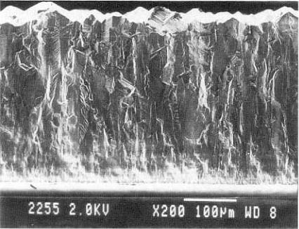
320 Carbon, Graphite, Diamond, and Fullerenes
Figure |
13.7. |
Cross-section |
of diamond |
coating |
(Photograph courtesy of |
|
Diamonex, |
Allentown, |
PA.) |
|
|
|
|
(WC, SiC) , and other metals such as Cu, Au and Ni and their alloys.[40] |
Of |
|||||||||||||||
particular |
industrial importance |
is the deposition |
on tool-steel substrate |
(see |
||||||||||||
Sec.5.0). |
Cubic boron nitride (c-BN) |
is also a suitable substrate |
with |
good |
||||||||||||
lattice matching |
but is only available |
as small |
single |
crystals. |
|
|
|
|
||||||||
The |
nucleation |
rate and |
the |
adhesion |
vary |
with the nature |
of |
the |
||||||||
substrate |
and appear |
to be related |
to the ability |
of the substrate |
material |
to |
||||||||||
form an |
intermediate |
carbide. |
Surface |
treatments |
such as |
etching |
or |
|||||||||
mechanical working (scratching |
with a diamond |
powder or diamond |
polish) |
|||||||||||||
help promote adhesion. |
|
|
|
|
|
|
|
|
|
|
|
|
|
|||
3.10 Oriented |
and Epitaxial Growth |
|
|
|
|
|
|
|
|
|
||||||
The |
properties |
of |
diamond |
are |
affected |
by |
|
impurities |
and |
lattice |
||||||
defects. |
In addition, |
they |
are influenced |
by |
crystal |
boundaries, |
especially |
|||||||||
CVD Diamond 321
if high-angle boundaries are dominant. A polycrystalline |
material |
such as |
CVD diamond has many such boundaries and various |
crystallite |
orienta- |
tions and grain sizes. As a result, its properties (particularly thermal, |
optical, |
|
and electrical) do not quite match those of single-crystal diamond, as shown
in Table 13.6.
The ability to deposit single-crystal diamond, or at least a material with
a high degree of crystalline orientation and with properties equal to the high-
purii |
single crystal material, would be an important factor in the develop- |
|||||
ment |
of CVD |
diamond in electronic, semiconductor, |
optical, |
and other |
||
applications. |
|
|
|
|
|
|
|
The epitaxial growth |
of single-crystal diamond |
by CVD |
could |
be |
|
accomplished |
by selecting |
a substrate with a crystal lattice parameters |
that |
|||
closely matches that of diamond and that would have the same atomic
bonding characteristic.t2s1 Single-crystal |
diamond is the |
only substrate |
|||
found suitable |
so far but it is limited |
by its small |
size and |
high cost. The |
|
development |
of other suitable substrates |
for epitaxial growth would allow |
|||
the production of diamond semiconductor wafers. |
Indications are that some |
||||
nickel alloys such as nickel-copper |
have |
a crystal structure that is suffi- |
|||
ciently close to that of diamond to allow the deposition of epitaxial films.t4’1
3.11 Morphology
The as-deposited surface of CVD diamond is rough as shown in Fig. 13.8 and a polishing step is required for many applications. Polishing to less than 5 nm radius without chipping or grain pulling is normally a difficult task. A smooth surface is now possible with the development of an ion-implan- tation technique with an energy range of up to 5000 keV, which softens the surface. This step is followed by a mechanical polishing with diamond paste.t42l
4.0PROPERTIES OF CVD DIAMOND
4.1Summary of Properties
CVD diamond is a recent material |
and, like single-crystal diamond, it |
|
is expensive |
and available only in small quantities and mostly in the form |
|
of coatings. |
As a result, the evaluation |
of its properties is still limited. The |
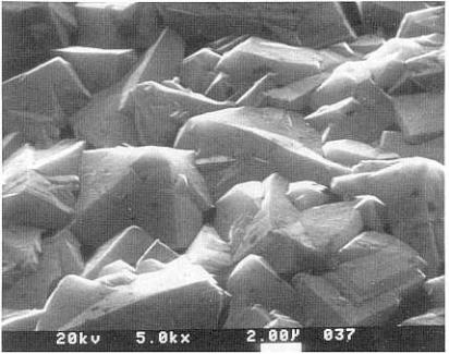
322 Carbon, Graphite, Diamond, and Fullerenes
Figure 13.8. Scanning electron micrographofCVD-diamond |
coating. (Photograph |
courtesy Norton Diamond Film, Northboro, MA.)
difficulty in testing, the effect of impurities and structural defects, and the differences between the various deposition processes may contribute to the uncertainty and spread found in the reported property values.
These properties are summarized and compared to single-crystal diamond in Table 13.6.[30]-[33][43]
4.2Thermal Properties
The mechanism of thermal conductivity in CVD diamond was reviewed in Secs. 3.6 and 3.9. In spite of crystal boundaries and resulting phonon scattering, the thermal conductivity is remarkably high which makes CVD diamond particularly suitable for heat-sink applications (see Sec.5.4).
CVD Diamond 323
Table 13.6. Properties of CVD diamond
|
|
|
|
|
|
CVD |
Single-Crystal |
||
|
|
|
|
|
|
Diamond |
Diamond |
||
Density, |
g/cm3 |
|
|
3.51 |
3.515 |
||||
Thermal |
conductivity |
at 25”C, W/m*K |
2100 |
2200 |
|||||
Thermal |
expansion |
|
coefficient |
|
|
|
|
||
x 1OS/C |
@ 25 - 200°C |
|
2.0 |
1.5 - 4.8 |
|||||
Bangap, |
eV |
|
|
|
5.45 |
5.45 |
|||
Index |
of refraction |
|
at 10 pm |
2.34 |
- 2.42 |
2.40 |
|||
Electrical |
resistivity, |
ohmcm |
lo’*- |
10’6 |
10’6 |
||||
Dielectric |
constant |
|
(45 MHz - 20 GHz) |
|
5.6 |
5.70 |
|||
Dielectric |
strength, |
|
V/cm |
106 |
|
106 |
|||
Loss tangent |
(45 MHz - 20 GHz) |
<0.0001 |
|
|
|||||
Saturated |
electron |
|
velocity |
2.7 |
|
2.7 |
|||
Carrier |
mobilities |
(cm*/Vs) |
|
|
|
|
|||
electron |
(n) |
|
|
1350 |
- 1500 |
2200 |
|||
positive |
hole |
(p) |
480 |
1600 |
|||||
Vickers |
hardness |
range*, kg/mm* |
5000 |
- 10000 |
5700 |
- 10400 |
|||
Coefficient of friction |
0.05 |
- 0.15 |
0.05 |
- 0.15 |
|||||
* Varies |
with |
crystal |
orientation |
|
|
|
|
||
4.3Optical Properties
In many optical,electronic, |
and opto-electronic |
applications, |
the |
main |
||||||||
emphasis |
is |
not |
so |
much |
on thickness |
since |
the |
required thickness is |
||||
submicron |
or |
at the |
most |
a few |
pm, but |
more |
on |
the |
deposition |
of |
pure |
|
diamond |
crystals |
without carbon, |
graphite, |
or metallic |
impurities. |
This |
has |
|||||
324 |
|
Carbon, |
Graphite, |
|
Diamond, |
and |
Fullerenes |
|
|
|
|
|
|
|||||||
yet |
to |
be |
achieved and |
present |
materials |
are opaque |
or |
translucent |
and |
|||||||||||
certainly |
not |
on |
par with |
gem-quality |
materialt3Q) (see |
Ch. 11, Sec. |
6.0). |
|||||||||||||
4.4 |
Electronic |
|
and |
Semiconductor |
|
Properties |
|
|
|
|
|
|
|
|||||||
|
The |
semiconductor |
|
characteristics |
of CVD |
diamond |
are |
similar |
to |
|||||||||||
those |
of the |
single crystal |
|
(see Ch. 11, Sec. 9.3). |
It is an indirect-bandgap, |
|||||||||||||||
high-temperaturesemiconductor |
which |
can be changed |
from |
an intrinsic |
to |
|||||||||||||||
an |
extrinsic |
semiconductor |
at |
room |
|
temperature |
by |
doping |
with |
other |
||||||||||
elements |
such |
as boron |
or phosphorus. |
f6)f2s) This |
doping |
is accomplished |
||||||||||||||
during |
deposition |
by introducing |
diborane |
(B2Hs) or phosphine (PHs) |
in the |
|||||||||||||||
deposition |
chamber. |
The |
semiconductor |
properties of CVD |
diamond |
are |
||||||||||||||
similar |
to those |
|
of the |
single crystal. |
|
|
|
|
|
|
|
|
|
|
||||||
4.5Mechanical Properties
The |
hardness |
of |
single-crystal |
diamond |
varies |
as a function |
of the |
||||||||
crystal |
orientation |
by |
almost |
a factor |
of two. |
This |
is |
also |
true of |
CVD |
|||||
diamond, |
and |
the |
hardness |
values |
depend |
on which |
crystal |
face |
is in |
||||||
contact |
with the |
indenter of the testing |
device. |
|
|
|
|
|
|
||||||
Wear |
resistance |
of CVD |
diamond |
is generally |
superior |
to that |
of the |
||||||||
single-crystal |
material |
since the wear of diamond occurs |
by chipping. |
Since |
|||||||||||
CVD diamond |
|
is |
a polycrystalline |
material, |
chipping |
stops |
at |
the |
grain |
||||||
boundary |
while, |
in a single-crystal, |
the |
entire |
crystal |
is sheared |
off. |
|
|||||||
4.6Chemical Properties
The chemical properties of CVD |
diamond |
are |
similar to those of the |
||
single-crystal material |
reviewed |
in Ch. |
11, Sec. |
11 |
.O. |
5.0 APPLICATIONS |
OF CVD |
DIAMOND |
|
|
|
5.1Status of CVD Diamond Applications
The applications of natural and high-pressure synthetic diamond were reviewed in Ch. 12. Although these applications have a very large market, particularly in gemstones, they are limited because of the small size and
|
|
|
|
|
|
|
|
|
|
|
|
|
|
|
|
|
|
CVD |
|
Diamond |
325 |
|||||
high cost |
of the |
crystals. |
CVD diamond, |
|
on the |
other |
hand, |
offers a broader |
||||||||||||||||||
potential |
since |
size, |
and |
eventually |
cost, |
are |
less |
of |
a limitation. |
|
It also |
|||||||||||||||
opensthe |
door |
to applications |
that |
would |
take full advantage |
of the |
intrinsic |
|||||||||||||||||||
properties |
of diamond |
in such |
areas assemiconductors, |
lasers, |
optics, |
opto- |
||||||||||||||||||||
electronics, |
wear |
and |
corrosion |
coatings, |
and |
others. |
|
|
|
|
|
|
|
|
||||||||||||
To estimate |
a market |
would |
be no more than a guessing |
|
game |
since |
||||||||||||||||||||
few applications |
at this time |
(1993) |
have |
reached the commercial |
stage and |
|||||||||||||||||||||
there |
is no historical |
background |
in patterns |
of growth |
and |
market |
size |
to |
||||||||||||||||||
buttress |
any predictions. |
|
|
|
|
|
|
|
|
|
|
|
|
|
|
|
|
|
|
|
|
|||||
Some |
actual |
and potential |
applications |
of CVD diamond |
|
are |
listed |
in |
||||||||||||||||||
Table 13.7.tsc)-tZ) |
|
|
|
|
|
|
|
|
|
|
|
|
|
|
|
|
|
|
|
|
|
|
||||
In the |
following |
sections, |
several |
typical |
applications |
|
are |
described. |
|
|||||||||||||||||
Table |
13.7. |
Actual and |
Potential |
Applications |
|
of CVD |
Diamond |
|
|
|
||||||||||||||||
Grinding, |
cutting: |
|
|
Inserts |
|
|
|
|
|
|
|
|
Oil |
drilling |
|
tools |
|
|
|
|||||||
|
|
|
|
|
|
|
Twist |
drills |
|
|
|
|
|
|
Slitter |
blades |
|
|
|
|||||||
|
|
|
|
|
|
|
Whetstones |
|
|
|
|
|
|
Surgical |
scalpels |
|
|
|||||||||
|
|
|
|
|
|
|
Industrial |
knives |
|
|
|
Saws |
|
|
|
|
|
|
|
|||||||
|
|
|
|
|
|
|
Circuit-board |
|
drills |
|
|
|
|
|
|
|
|
|
|
|
||||||
Wear |
parts: |
|
|
|
|
Bearings |
|
|
|
|
|
|
|
Engine |
parts |
|
|
|
||||||||
|
|
|
|
|
|
|
Jet-nozzle |
coatings |
|
|
Medical |
implants |
|
|
||||||||||||
|
|
|
|
|
|
|
Slurry |
valves |
|
|
|
|
|
Ball bearings |
|
|
|
|||||||||
|
|
|
|
|
|
|
Extrusion |
dies |
|
|
|
|
|
Drawing |
dies |
|
|
|
||||||||
|
|
|
|
|
|
|
Abrasive |
pump |
seals |
|
Textile |
|
machinery |
|
||||||||||||
|
|
|
|
|
|
|
Computer |
disk |
coatings |
|
|
|
|
|
|
|
|
|
||||||||
Acoustical: |
|
|
|
|
Speaker |
diaphragms |
|
|
|
|
|
|
|
|
|
|
|
|||||||||
Diffusion, |
corrosion: |
|
Crucibles |
|
|
|
|
|
|
|
Fiber |
coatings |
|
|
|
|||||||||||
|
|
|
|
|
|
|
Ion |
barriers |
(sodium) |
|
|
Reaction |
vessels |
|
|
|||||||||||
Optical |
coatings: |
|
|
Laser |
protection |
|
|
|
|
Antireflection |
|
|
|
|||||||||||||
|
|
|
|
|
|
|
Fiber |
optics |
|
|
|
|
|
|
UV to IR windows |
|
||||||||||
|
|
|
|
|
|
|
X-ray |
windows |
|
|
|
|
|
Radomes |
|
|
|
|
|
|||||||
Photonic |
devices: |
|
|
Radiation |
detectors |
|
|
Switches |
|
|
|
|
|
|||||||||||||
Thermal |
management: |
|
Heat-sink |
diodes |
|
|
|
Thermal |
printers |
|
|
|||||||||||||||
|
|
|
|
|
|
|
Heat-sink |
PC |
boards |
|
|
Target |
|
heat-sinks |
|
|
||||||||||
Semiconductor: |
|
|
|
High-power |
transistors |
|
Field-effect |
|
transistors |
|||||||||||||||||
|
|
|
|
|
|
|
High-power |
microwave |
|
UV sensors |
|
|
|
|
||||||||||||
|
|
|
|
|
|
|
Photovoltaic |
elements |
|
|
|
|
|
|
|
|
|
|
||||||||