

9 Additional Circuit Designs
In the preceding chapters, we saw a series of complete design examples utilizing VHDL code. Each design included:
Top-level diagram of the circuit, with description;
Review of basic concepts whenever necessary;
Complete VHDL code;
Simulation results; and
Additional comments when needed.
This chapter concludes Part I of the book. In it, a series of additional design examples are presented. These examples, like all the other designs shown so far, are also at the circuit level (that is, self-contained in the main code). In Part II, we will do the same; that is, we will conclude Part II with a chapter containing additional system design examples.
The designs presented in this chapter are the following:
Barrel shifter (section 9.1)
Signed and unsigned comparators (section 9.2)
Carry ripple and carry look ahead adders (section 9.3)
Fixed-point division (section 9.4)
Vending machine controller (section 9.5)
Serial data receiver (section 9.6)
Parallel-to-serial converter (section 9.7)
Playing with a SSD (section 9.8)
Signal generators (section 9.9)
Memories (section 9.10)
Finally, a list of problems is also included (section 9.11).
Note: A complete list of all designs presented in the book is shown in section 1.5.
9.1Barrel Shifter
The diagram of a barrel shifter is shown in figure 9.1. The input is an 8-bit vector. The output is a shifted version of the input, with the amount of shift defined by the ‘‘shift’’ input (from 0 to 7). The circuit consists of three individual barrel shifters, each similar to that seen in example 6.9. Notice that the first barrel has only one ‘0’
TLFeBOOK

188
inp(7)
|
|
|
|
|
|
MUX |
|
|
|
|
|
|
|
|
|
|
|
|
|
|
|
|
|
|
|
|
|
|
|
|
||
|
|
|
|
|
|
|
|
|
|
|
|
|
|
|
|
|
|
|
|
|
|
|
|
|
|
|
|
|
|
|
|
|
inp(6) |
|
|
|
|
|
|
|
|
|
|
|
|
|
|
|
|
|
MUX |
|
|
|
|
|
|
|
|
|
|
||||
|
|
|
|
|
|
|
|
|
|
|
|
|
|
|
|
|
|
|
|
|
|
|
|
|
|
|
||||||
|
|
|
|
|
|
|
|
|
|
|
|
|
|
|
|
|
|
|
|
|
|
|
|
|
|
|
|
MUX |
||||
|
|
|
|
|
|
|
|
|
|
|
|
|
|
|
|
|
|
|
|
|
|
|
|
|
|
|
|
|
|
|
|
|
|
|
|
|
|
|
MUX |
|
|
|
|
|
|
|
|
|
|
|
|
|
|
|
|
|
|
|
|
|
|
|
|
||
|
|
|
|
|
|
|
|
|
|
|
|
|
|
|
|
|
|
|
|
|
|
|
|
|
|
|
|
|
|
|
|
|
inp(5) |
|
|
|
|
|
|
|
|
|
|
|
|
|
|
|
|
MUX |
|
|
|
|
|
|
|
|
|
|
|
||||
|
|
|
|
|
|
|
|
|
|
|
|
|
|
|
|
|
|
|
|
|
|
|
|
|||||||||
|
|
|
|
|
|
|
|
|
|
|
|
|
|
|
|
|
|
|
|
|
|
|
|
|
|
|
|
|
|
|
|
|
|
|
|
|
|
|
|
|
|
|
|
|
|
|
|
|
|
|
|
|
|
|
|
|
|
|
|
|
MUX |
||||
|
|
|
|
|
|
|
|
|
|
|
|
|
|
|
|
|
|
|
|
|
|
|
|
|
|
|
|
|
|
|
|
|
|
|
|
|
|
|
|
|
|
|
|
|
|
|
|
|
|
|
|
|
|
|
|
|
|
|
|
|
|
|
|
|
|
|
|
|
|
|
|
MUX |
|
|
|
|
|
|
|
|
|
|
|
|
|
|
|
|
|
|
|
|
|
|
|
|
||
|
|
|
|
|
|
|
|
|
|
|
|
|
|
|
|
|
|
|
|
|
|
|
|
|
|
|
|
|
|
|
|
|
inp(4) |
|
|
|
|
|
|
|
|
|
|
|
|
|
|
|
|
|
MUX |
|
|
|
|
|
|
|
|
|
|
||||
|
|
|
|
|
|
|
|
|
|
|
|
|
|
|
|
|
|
|
|
|
|
|
|
|
||||||||
|
|
|
|
|
|
|
|
|
|
|
|
|
|
|
|
|
|
|
|
|
|
|
|
|
|
|
|
|
|
|
|
|
|
|
|
|
|
|
|
|
|
|
|
|
|
|
|
|
|
|
|
|
|
|
|
|
|
|
|
|
MUX |
||||
|
|
|
|
|
|
|
|
|
|
|
|
|
|
|
|
|
|
|
|
|
|
|
|
|
|
|
|
|
|
|
|
|
|
|
|
|
|
|
MUX |
|
|
|
|
|
|
|
|
|
|
|
|
|
|
|
|
|
|
|
|
|
|
|
|
||
|
|
|
|
|
|
|
|
|
|
|
|
|
|
|
|
|
|
|
|
|
|
|
|
|
|
|
|
|
|
|
|
|
inp(3) |
|
|
|
|
|
|
|
|
|
|
|
|
|
|
|
|
|
MUX |
|
|
|
|
|
|
|
|
||||||
|
|
|
|
|
|
|
|
|
|
|
|
|
|
|
|
|
|
|
|
|
|
|
|
|
|
|
|
|
|
|
|
|
|
|
|
|
|
|
|
|
|
|
|
|
|
|
|
|
|
|
|
|
|
|
|
|
|
|
|
|
MUX |
||||
|
|
|
|
|
|
|
|
|
|
|
|
|
|
|
|
|
|
|
|
|
|
|
|
|
|
|
|
|
|
|
|
|
|
|
|
|
|
|
|
|
|
|
|
|
|
|
|
|
|
|
|
|
|
|
|
|
|
|
|
|
|
|
|
|
|
|
|
|
|
|
|
MUX |
|
|
|
|
|
|
|
|
|
|
|
|
|
|
|
|
|
|
|
|
|
|
|
|
||
|
|
|
|
|
|
|
|
|
|
|
|
|
|
|
|
|
|
|
|
|
|
|
|
|
|
|
|
|
|
|||
|
|
|
|
|
|
|
|
|
|
|
|
|
|
|
|
|
|
|
|
|
|
|
|
|
|
|
|
|
|
|
|
|
inp(2) |
|
|
|
|
|
|
|
|
|
|
|
|
|
|
|
|
|
MUX |
|
|
|
|
|
|
|
|
||||||
|
|
|
|
|
|
|
|
|
|
|
|
|
|
|
|
|
|
|
|
|
|
|
|
|
|
|
|
|
|
|
|
|
|
|
|
|
|
|
|
|
|
|
|
|
|
|
|
|
|
|
|
|
|
|
|
|
|
|
‘0’ |
|
MUX |
||||
|
|
|
|
|
|
|
|
|
|
|
|
|
|
|
|
|
|
|
|
|
|
|
|
|
|
|
||||||
|
|
|
|
|
|
|
|
|
|
|
|
|
|
|
|
|
|
|
|
|
|
|
|
|
|
|
|
|
||||
|
|
|
|
|
|
MUX |
|
|
|
|
|
|
|
|
||||||||||||||||||
|
|
|
|
|
|
|
|
|
|
|
|
|
|
|
|
|
|
|
|
|
|
|
|
|
|
|
|
|||||
|
|
|
|
|
|
|
|
|
|
|
|
|
|
|
|
|
|
|
|
|
|
|
|
|
|
|
|
|
|
|
|
|
inp(1) |
|
|
|
|
|
|
|
|
|
|
|
|
|
|
|
|
|
MUX |
|
|
|
|
|
|
|
|
|
|
||||
|
|
|
|
|
|
|
|
|
|
|
|
|
|
|
|
|
|
|
|
|
|
|
|
|
||||||||
|
|
|
|
|
|
|
|
|
|
|
|
|
|
|
|
|
|
|
|
|
|
|
|
|
|
|
|
|
|
|
|
|
|
|
|
|
|
|
|
|
|
|
|
|
|
|
|
|
|
|
|
|
|
|
|
|
|
|
‘0’ |
|
MUX |
||||
|
|
|
|
|
|
|
|
|
|
|
|
|
|
|
|
|
|
|
|
|
|
|
|
|
|
|
|
|
||||
|
|
|
|
|
|
MUX |
|
|
|
|
|
|
|
|
||||||||||||||||||
|
|
|
|
|
|
|
|
|
|
|
|
|
|
|
|
|
|
|
|
|
|
|
|
|
|
|
|
|||||
|
|
|
|
|
|
|
|
|
|
|
|
|
|
|
|
|
|
|
|
|
|
|
|
|
|
|
|
|
|
|
|
|
inp(0) |
|
|
|
|
|
|
|
|
|
|
|
|
|
|
|
|
|
MUX |
|
|
|
|
|
|
|
|
||||||
|
|
|
|
|
|
|
|
|
|
|
|
|
|
|
|
|
|
|
|
|
|
|
|
|
|
|
|
|
|
|
|
|
|
|
|
|
|
|
|
|
|
|
|
|
|
|
‘0’ |
|
|
|
|
|
|
|
|
|
|
|
‘0’ |
|
MUX |
||||
|
|
|
|
|
|
|
|
|
|
|
|
|
|
|
|
|
|
|
|
|
|
|
|
|
|
|||||||
|
|
|
|
|
|
|
|
|
|
|
|
|
|
|
|
|
|
|
|
|
|
|
|
|
|
|
|
|
||||
|
|
|
|
|
|
MUX |
|
|
|
|
|
|
|
|
||||||||||||||||||
|
|
|
|
|
|
|
|
|
|
|
|
|
|
|
|
|
|
|
|
|
|
|
|
|
|
|
|
|||||
|
|
|
|
|
|
|
|
|
|
|
|
|
|
|
|
|
|
|
|
|
|
|
|
|
|
|
|
|
|
|
|
|
|
‘0’ |
|
|
|
|
|
|
|
|
|
|
|
|
MUX |
|
|
|
|
|
|
|
|
|
|||||||||
|
|
|
|
|
|
|
|
|
|
|
|
|
|
|
|
|
|
|
|
|
|
|
||||||||||
shift(0) |
|
|
|
|
|
|
|
|
|
|
|
|
|
|
‘0’ |
|
|
|
|
|
|
|
|
|
|
|
‘0’ |
|
MUX |
|||
|
|
|
|
|
|
|
|
|
|
|
|
|
|
|
|
|
|
|
|
|
|
|
|
|
|
|||||||
|
|
|
|
|
|
|
|
|
|
|
|
|
|
|
|
|
|
|
|
|
||||||||||||
|
|
|
|
|
|
|
|
|
|
|
|
|
|
|
|
|
|
|
|
|
|
|
|
|
|
|
|
|
|
|
||
|
|
|
|
|
|
|
|
|
|
|
|
|
|
|
|
|
|
|
|
|
|
|
|
|
|
|
|
|
|
|
||
shift(1) |
|
|
|
|
|
|
|
|
|
|
|
|
|
|
|
|
|
|
|
|
|
|
|
|
|
|
|
|
|
|
||
|
|
|
|
|
|
|
|
|
|
|
|
|
|
|
|
|
|
|
|
|
|
|
|
|
|
|
|
|
|
|
|
|
shift(2) |
|
|
|
|
|
|
|
|
|
|
|
|
|
|
|
|
|
|
|
|
|
|
|
|
|
|
|
|
|
|
|
|
|
|
|
|
|
|
|
|
|
|
|
|
|
|
|
|
|
|
|
|
|
|
|
|
|
|
|
|
|
|
|
|
|
Chapter 9
 outp(7)
outp(6)
 outp(5)
 outp(4)
 outp(3)
 outp(2)
 outp(1)
 outp(0)
Figure 9.1
Barrel shifter.
TLFeBOOK
Additional Circuit Designs |
189 |
Figure 9.2
Simulation results from barrel shifter of figure 9.1.
connected to one of the multiplexers (bottom left corner), while the second has two, and the third has four. For larger vectors, we would just keep doubling the number of ‘0’ inputs. If shift ¼ ‘‘001’’, for example, then only the first barrel should cause a shift; on the other hand, if shift ¼ ‘‘111’’, then all barrels should cause a shift.
A VHDL code for the circuit of figure 9.1 is presented below. Simulation results, verifying the functionality of the circuit, are shown in figure 9.2. As can be seen in the latter, the output is equal to the input when shift ¼ 0 (that is, shift ¼ ‘‘000’’). It can also be seen that, as long as no bit of value ‘1’ is shifted out of the barrel, the output is equal to the input multiplied by 2 (1 shift) when shift ¼ 1 (‘‘001’’), multiplied by 4 (2 shifts) when shift ¼ 2 (‘‘010’’), multiplied by 8 (3 shifts) when shift ¼ 3 (‘‘011’’), and so on.
1 ---------------------------------------------
2LIBRARY ieee;
3 USE ieee.std_logic_1164.all;
4 ---------------------------------------------
5ENTITY barrel IS
6PORT ( inp: IN STD_LOGIC_VECTOR (7 DOWNTO 0);
7shift: IN STD_LOGIC_VECTOR (2 DOWNTO 0);
8 |
outp: OUT STD_LOGIC_VECTOR (7 DOWNTO 0)); |
9 |
END barrel; |
10 |
--------------------------------------------- |
11 |
ARCHITECTURE behavior OF barrel IS |
12BEGIN
13PROCESS (inp, shift)
14VARIABLE temp1: STD_LOGIC_VECTOR (7 DOWNTO 0);
15VARIABLE temp2: STD_LOGIC_VECTOR (7 DOWNTO 0);
16BEGIN
TLFeBOOK
190 |
Chapter 9 |
17---- 1st shifter -----
18IF (shift(0)='0') THEN
19temp1 := inp;
20ELSE
21temp1(0) := '0';
22FOR i IN 1 TO inp'HIGH LOOP
23temp1(i) := inp(i-1);
24END LOOP;
25END IF;
26---- 2nd shifter -----
27IF (shift(1)='0') THEN
28temp2 := temp1;
29ELSE
30FOR i IN 0 TO 1 LOOP
31temp2(i) := '0';
32END LOOP;
33FOR i IN 2 TO inp'HIGH LOOP
34temp2(i) := temp1(i-2);
35END LOOP;
36END IF;
37---- 3rd shifter -----
38IF (shift(2)='0') THEN
39outp <= temp2;
40ELSE
41FOR i IN 0 TO 3 LOOP
42outp(i) <= '0';
43END LOOP;
44FOR i IN 4 TO inp'HIGH LOOP
45outp(i) <= temp2(i-4);
46END LOOP;
47END IF;
48END PROCESS;
49END behavior;
50---------------------------------------------
TLFeBOOK
Additional Circuit Designs |
191 |
a (n:0) |
|
|
a>b |
x1 |
|
||||
|
|
|
a=b |
x2 |
b (n:0) |
|
|
a<b |
x3 |
|
|
|
||
|
|
|
|
|
Figure 9.3
Comparator.
9.2Signed and Unsigned Comparators
Figure 9.3 shows the top-level diagram of a comparator. The size of the vectors to be compared is generic (n þ 1). Three outputs must be provided: one corresponding to a > b, another to a ¼ b, and finally one relative to a < b. Three solutions are presented: the first considers a and b as signed numbers, while the other two consider them as unsigned values. Simulation results are also included.
Signed Comparator
Notice the presence of the std_logic_arith package in the code below (line 4), which is necessary to operate with SIGNED (or UNSIGNED) data types (a and b were declared as SIGNED numbers in line 8).
1 ---- Signed Comparator: ----------------
2LIBRARY ieee;
3USE ieee.std_logic_1164.all;
4 |
USE ieee.std_logic_arith.all; -- necessary! |
5 |
---------------------------------------- |
6ENTITY comparator IS
7GENERIC (n: INTEGER := 7);
8PORT (a, b: IN SIGNED (n DOWNTO 0);
9 |
x1, |
x2, x3: OUT STD_LOGIC); |
10 |
END comparator; |
|
11 |
---------------------------------------- |
|
12 |
ARCHITECTURE |
signed OF comparator IS |
13BEGIN
14x1 <= '1' WHEN a > b ELSE '0';
15x2 <= '1' WHEN a = b ELSE '0';
16x3 <= '1' WHEN a < b ELSE '0';
17END signed;
18 ----------------------------------------
TLFeBOOK

192 |
Chapter 9 |
Figure 9.4
Simulation result of signed comparator of figure 9.3.
Simulation results are shown in figure 9.4. As can be seen, 127 > 0, but 128 < 0 and also 255 < 0 (because in 2’s complement notation 127 is the decimal 127 itself, but 128 is the decimal 128, and 255 is indeed 1).
Unsigned Comparator #1
The VHDL code below is the counterpart of the code just presented (signed comparator). Notice again the presence of the std_logic_arith package (line 4), which is necessary to operate with UNSIGNED (or SIGNED) data types (a and b were declared as UNSIGNED numbers in line 8).
1 ---- Unsigned Comparator #1: -----------
2LIBRARY ieee;
3USE ieee.std_logic_1164.all;
4 |
USE ieee.std_logic_arith.all; -- necessary! |
5 |
---------------------------------------- |
6ENTITY comparator IS
7GENERIC (n: INTEGER := 7);
8 PORT (a, b: IN UNSIGNED (n DOWNTO 0);
9 x1, x2, x3: OUT STD_LOGIC);
10 END comparator;
11 ----------------------------------------
12 ARCHITECTURE unsigned OF comparator IS
13BEGIN
14x1 <= '1' WHEN a > b ELSE '0';
15x2 <= '1' WHEN a = b ELSE '0';
16x3 <= '1' WHEN a < b ELSE '0';
17END unsigned;
18 ----------------------------------------
TLFeBOOK

Additional Circuit Designs |
193 |
Figure 9.5
Simulation result of unsigned comparator of figure 9.3.
Unsigned Comparator #2
Unsigned comparators can also be implemented with STD_LOGIC_VECTORS, in which case there is no need to declare the std_logic_arith package. A solution of this kind is presented below.
1 ---- Unsigned Comparator #2: -----------
2LIBRARY ieee;
3 USE ieee.std_logic_1164.all;
4 ----------------------------------------
5ENTITY comparator IS
6GENERIC (n: INTEGER := 7);
7PORT (a, b: IN STD_LOGIC_VECTOR (n DOWNTO 0);
8 |
x1, |
x2, x3: OUT STD_LOGIC); |
9 |
END comparator; |
|
10 |
---------------------------------------- |
|
11 |
ARCHITECTURE |
unsigned OF comparator IS |
12BEGIN
13x1 <= '1' WHEN a > b ELSE '0';
14x2 <= '1' WHEN a = b ELSE '0';
15x3 <= '1' WHEN a < b ELSE '0';
16END unsigned;
17 ----------------------------------------
Simulation results (from either unsigned comparator) are shown in figure 9.5. Contrary to figure 9.4, now 128 and 255 are indeed bigger than zero.
TLFeBOOK

194 |
Chapter 9 |
|
|
|
a(0) b(0) |
|
|
a(1) b(1) |
|
|
|
a(2) b(2) |
|
|
a(3) b(3) |
|
|
|
|
|
|
||||||||||||||
|
|
|
|
|
|
|
|
|
|
|
|
a b |
cin |
s |
cout |
||||||||||||||||||
|
|
|
|
|
|
|
|
|
|
|
|
|
|
|
|
|
|
|
|
|
|
|
|
|
|
|
|
|
|
||||
|
|
|
|
|
|
|
|
|
|
|
|
|
|
|
|
|
|
|
|
|
|
|
|
|
|
|
|
|
|
0 0 |
0 |
0 |
0 |
|
|
|
|
|
|
|
|
|
|
|
|
|
|
|
|
|
|
|
|
|
|
|
|
|
|
|
|
|
|
0 1 |
0 |
1 |
0 |
cin |
|
|
|
FAU |
|
|
|
|
|
FAU |
|
|
|
|
FAU |
|
|
|
|
FAU |
|
cout |
1 0 |
0 |
1 |
0 |
|||||||
|
|
c(1) |
|
|
|
|
|
|
|||||||||||||||||||||||||
c(0) |
c(2) |
|
|
|
|||||||||||||||||||||||||||||
|
|
|
|
|
|
|
|
|
|
|
|
|
|
|
|
|
|
c(3) |
|
|
|
|
|
c(4) |
1 1 |
0 |
0 |
1 |
|||||
|
|
|
|
|
|
|
|
|
|
|
|
|
|
|
|
|
|
|
|
|
|
|
|
|
|
|
|
|
|
0 0 |
1 |
1 |
0 |
|
|
|
|
|
|
|
|
|
|
|
|
|
|
|
|
|
|
|
|
|
|
|
|
|
|
|
|
|
|
0 1 |
1 |
0 |
1 |
|
|
|
|
|
|
|
|
|
|
|
|
|
|
|
|
|
|
|
|
|
|
|
|
|
|
|
|
|
|
||||
|
|
|
|
s(0) |
|
|
|
s(1) |
|
|
|
|
s(2) |
|
|
s(3) |
|
|
1 0 |
1 |
0 |
1 |
|||||||||||
|
|
|
|
|
|
|
|
|
|
|
|
|
|
|
1 1 |
1 |
1 |
1 |
|||||||||||||||
Figure 9.6
4-bit carry ripple adder and truth table of Full Adder Unit (FAU).
9.3Carry Ripple and Carry Look Ahead Adders
Carry ripple and carry look ahead are two classical approaches to the design of adders. The former has the advantage of requiring less hardware, while the latter is faster. Both approaches are discussed below.
Carry Ripple Adder
Figure 9.6 shows a 4-bit unsigned carry ripple adder. For each bit, a full adder unit (FAU, section 1.4) is employed. The truth table of the FAU is also shown. In it, a and b represent the input bits, cin is the carry-in bit, s is the sum bit, and cout is the carry-out bit. s must be high whenever the number of inputs that are high is odd (parity function), while cout must be high when two or more inputs are high (majority function). Notice in figure 9.6 that each FAU relies on the carry bit produced by the previous stage. This approach minimizes the size of the circuitry, at the expense of increased propagation delay.
Based on the truth table of figure 9.6, a very simple way of computing s and cout is the following:
s ¼ a XOR b XOR cin
cout ¼ (a AND b) OR (a AND cin) OR (b AND cin)
Therefore, a VHDL implementation of the carry ripple adder is straightforward. The solution shown below works for any number (n) of input bits, defined by means of a GENERIC statement in line 5. Simulation results from the circuit synthesized with the code below are shown in figure 9.7.
1LIBRARY ieee;
2USE ieee.std_logic_1164.all;
TLFeBOOK

Additional Circuit Designs |
195 |
Figure 9.7
Simulation results from the carry ripple adder of figure 9.6.
3 ---------------------------------------------
4ENTITY adder_cripple IS
5GENERIC (n: INTEGER := 4);
6PORT ( a, b: IN STD_LOGIC_VECTOR (n-1 DOWNTO 0);
7cin: IN STD_LOGIC;
8s: OUT STD_LOGIC_VECTOR (n-1 DOWNTO 0);
9 |
cout: OUT STD_LOGIC); |
10 |
END adder_cripple; |
11 |
--------------------------------------------- |
12 |
ARCHITECTURE adder OF adder_cripple IS |
13SIGNAL c: STD_LOGIC_VECTOR (n DOWNTO 0);
14BEGIN
15c(0) <= cin;
16G1: FOR i IN 0 TO n-1 GENERATE
17s(i) <= a(i) XOR b(i) XOR c(i);
18c(i+1) <= (a(i) AND b(i)) OR
19 |
(a(i) |
AND |
c(i)) OR |
20 |
(b(i) |
AND |
c(i)); |
21END GENERATE;
22cout <= c(n);
23END adder;
24 ---------------------------------------------
Pre-defined ‘‘B’’ Operator
We have already seen that an adder can be implemented directly with the ‘‘þ’’ (addition) operator (section 4.1). In this case, a carry ripple type of solution will be normally implemented by the synthesizer. If, however, if we want the solution to be of a certain type (like the one presented next), then an explicit code must be written.
TLFeBOOK

196 |
Chapter 9 |
s(0) |
s(1) |
s(2) |
s(3) |
a(0) b(0) |
a(1) b(1) |
a(2) b(2) |
a(3) b(3) |
|
PGU |
PGU |
PGU |
PGU |
|
|
p(0) g(0) |
p(1) g(1) |
p(2) g(2) |
p(3) g(3) |
|
cin |
|
c(1) |
c(2) |
c(3) |
|
c(0) |
|
CLAU |
c(4) |
cout |
|
|
|
|
|
|
Figure 9.8
4-bit carry look ahead adder.
Carry Look Ahead Adder
A diagram of a 4-bit carry look ahead adder is shown in figure 9.8. Its implementation is based on the generate and propagate concept, which gives the circuit higher speed than its carry ripple adder counterpart (at the expense of more silicon area).
Consider two input bits, a and b. The generate (g) and propagate (p) signals are defined as:
g ¼ a AND b
p ¼ a XOR b
Notice that such signals can be computed in advance, because neither depends on the carry bit.
If we consider now two input vectors, a ¼ a(n 1) . . . a(1)a(0) and b ¼ b(n 1)
. . . b(1)b(0), then the corresponding generate and propagate vectors are g ¼ g(n 1)
. . . g(1)g(0) and p ¼ p(n 1) . . . p(1)p(0), where
g( j) ¼ a( j) AND b( j)
p( j) ¼ a( j) XOR b( j)
Let us consider now the carry vector, c ¼ c(n 1) . . . c(1)c(0). The carry bits can be computed from g and p:
c(0) C cin
c(1) ¼ c(0)p(0) þ g(0)
TLFeBOOK
Additional Circuit Designs |
197 |
c(2) ¼ c(0)p(0)p(1) þ g(0)p(1) þ g(1)
c(3) ¼ c(0)p(0)p(1)p(2) þ g(0)p(1)p(2) þ g(1)p(2) þ g(2), etc.
Notice that, contrary to the carry ripple adder, each carry bit above is computed independently; that is, none of the expressions above depends on preceding carry computations, and that is the reason why this circuit is faster. On the other hand, the hardware complexity grows very fast, limiting this approach to just a few bits (typically four). Larger carry look ahead adders can be implemented by associating such 4-bit-or-so units.
The implementation of the adder of figure 9.8 is now straightforward. The PGU (Propagate—Generate Unit) computes p and g (four units are required), plus the actual sum (s), while the CLAU (Carry Look Ahead Unit) computes the carry bits.
Note: In order to construct bigger carry look ahead adders, the CLAU block of figure 9.8 must posses Group Propagate (GP) and Group Generate (GG) outputs, which were omitted in the figure because this implementation is intended for four bits only.
1 ---------------------------------------------
2LIBRARY ieee;
3 USE ieee.std_logic_1164.all;
4 ---------------------------------------------
5ENTITY CLA_Adder IS
6PORT ( a, b: IN STD_LOGIC_VECTOR (3 DOWNTO 0);
7cin: IN STD_LOGIC;
8s: OUT STD_LOGIC_VECTOR (3 DOWNTO 0);
9 |
cout: OUT STD_LOGIC); |
10 |
END CLA_Adder; |
11 |
--------------------------------------------- |
12 |
ARCHITECTURE CLA_Adder OF CLA_Adder IS |
13SIGNAL c: STD_LOGIC_VECTOR (4 DOWNTO 0);
14SIGNAL p: STD_LOGIC_VECTOR (3 DOWNTO 0);
15SIGNAL g: STD_LOGIC_VECTOR (3 DOWNTO 0);
16BEGIN
17---- PGU: ---------------------------------
18G1: FOR i IN 0 TO 3 GENERATE
19p(i) <= a(i) XOR b(i);
20g(i) <= a(i) AND b(i);
21s(i) <= p(i) XOR c(i);
TLFeBOOK
198 |
Chapter 9 |
22END GENERATE;
23---- CLAU: --------------------------------
24c(0) <= cin;
25c(1) <= (cin AND p(0)) OR
26 |
|
g(0); |
|
27 |
c(2) |
<= (cin AND p(0) AND |
p(1)) OR |
28 |
|
(g(0) AND p(1)) OR |
|
29 |
|
g(1); |
|
30 |
c(3) |
<= (cin AND p(0) AND p(1) AND p(2)) OR |
|
31 |
|
(g(0) AND p(1) AND p(2)) OR |
|
32 |
|
(g(1) AND p(2)) OR |
|
33 |
|
g(2); |
|
34 |
c(4) |
<= (cin AND p(0) AND p(1) AND p(2) AND p(3)) OR |
|
35 |
|
(g(0) AND p(1) AND p(2) AND p(3)) OR |
|
36 |
|
(g(1) AND p(2) AND p(3)) OR |
|
37 |
|
(g(2) AND p(3)) OR |
|
38 |
|
g(3); |
|
39cout <= c(4);
40END CLA_Adder;
41---------------------------------------------
Qualitatively, the simulation results obtained from the circuit synthesized with the code above are similar to those from the carry ripple adder presented in figure 9.7.
9.4 Fixed-Point Division
We saw in chapter 4 that the pre-defined ‘‘/’’ (division) operator accepts only power of two divisors, that is, it is indeed a ‘‘shift’’ operator. In this section, we will discuss the implementation of generic division, in which the dividend and divisor can be any integer. We start by describing the division algorithm, then we present two VHDL solutions followed by simulation results.
Division Algorithm
Say that we want to calculate y ¼ a/b, where a, b, and y have the same number (n þ 1) of bits. The algorithm is illustrated in figure 9.9, for a ¼ ‘‘1011’’ (decimal 11) and b ¼ ‘‘0011’’ (decimal 3), from which we expect y ¼ ‘‘0011’’ (decimal 3) and remainder ‘‘0010’’ (decimal 2). We first create a shifted version of b, whose length is 2n þ 1 bits (shown in the b-related column in figure 9.9). b_inp(i) is simply b shifted to the left by i positions (notice the underscored characters in the b-related column).
TLFeBOOK
Additional Circuit Designs |
199 |
Index |
|
a-related |
Comparison |
b-related |
y (quotient) |
Operation on 1st column |
(i) |
|
input (a_inp) |
|
input (b_inp) |
|
|
|
|
|
|
|
|
|
3 |
|
1011 |
< |
0011000 |
0 |
none |
2 |
|
1011 |
< |
0001100 |
0 |
none |
1 |
|
1011 |
> |
0000110 |
1 |
a_inp(i)-b_inp(i) |
0 |
|
0101 |
> |
0000011 |
1 |
a_inp(i)-b_inp(i) |
|
|
|
|
|
|
|
|
|
0010 (rem) |
|
|
|
|
|
|
|
|
|
|
|
Figure 9.9 |
|
|
|
|
|
|
Division algorithm. |
|
|
|
|
||
The computation of the quotient is performed as follows. Starting from the top of the table, we compare a_inp(i) with b_inp(i). If the former is bigger than or equal to the latter, than y(i) ¼ ‘1’ and b_inp(i) is subtracted from a_inp(i); otherwise, y(i) ¼ ‘0’ and we simply proceed to the next line. After n þ 1 iterations, the computation is completed and the value left in a_inp is the remainder.
Note: It is obvious that, to subtract b_inp from a_inp, the number of bits of a_inp cannot be less than that of b_inp, so the actual length of a_inp must be increased, which is attained by simply filling a_inp with n ‘0’s on its left-hand side (‘0’s not shown in figure 9.9).
Another way of presenting the division algorithm is the following. We multiply b by 2**n, where n þ 1 is the number of bits. This, of course, corresponds to shifting b n positions to the left, but without throwing out any of its bits (so the new b-vector must be n bits longer than the original vector). If a is bigger than the new b, then y(n) ¼ ‘1’, and b (the new value) must be subtracted from a; otherwise, y(n) ¼ ‘0’. Now we move to the next iteration. We multiply b (the original value) by 2**(n 1), which is equivalent to shifting the original vector n 1 positions to the left, or shifting the value of b just used in the previous computation back one position to the right. Then we compare it to a, as we did before, to decide whether y(n 1) should be ‘1’ or ‘0’, and so on.
VHDL Dividers
Below are two solutions for the division problem. Both use sequential code: IF is used in the first, while LOOP plus IF are employed in the second. The first solution is a step-by-step code, so the division algorithm described above can be clearly observed. The second is more compact and is also generic (notice that n was defined
TLFeBOOK

200 |
Chapter 9 |
Figure 9.10
Simulation results of divider (for 4-bit operands).
by means of a GENERIC statement in line 6). The solutions include also a b ¼ 0 check routine.
Simulation results are shown in figure 9.10.
1 ----- Solution 1: step-by-step -------------------
2LIBRARY ieee;
3 USE ieee.std_logic_1164.all;
4 --------------------------------------------------
5ENTITY divider IS
6PORT ( a, b: IN INTEGER RANGE 0 TO 15;
7y: OUT STD_LOGIC_VECTOR (3 DOWNTO 0);
8rest: OUT INTEGER RANGE 0 TO 15;
9 |
err : OUT STD_LOGIC); |
|
10 |
END divider; |
|
11 |
-------------------------------------------------- |
|
12 |
ARCHITECTURE |
rtl OF divider IS |
13BEGIN
14PROCESS (a, b)
15VARIABLE temp1: INTEGER RANGE 0 TO 15;
16VARIABLE temp2: INTEGER RANGE 0 TO 15;
17BEGIN
18----- Error and initialization: -------
19temp1 := a;
20temp2 := b;
21IF (b=0) THEN err <= '1';
22ELSE err <= '0';
23END IF;
24----- y(3): ---------------------------
TLFeBOOK
Additional Circuit Designs |
201 |
25IF (temp1 >= temp2 * 8) THEN
26y(3) <= '1';
27temp1 := temp1 - temp2*8;
28ELSE y(3) <= '0';
29END IF;
30----- y(2): ---------------------------
31IF (temp1 >= temp2 * 4) THEN
32y(2) <= '1';
33temp1 := temp1 - temp2 * 4;
34ELSE y(2) <= '0';
35END IF;
36----- y(1): ---------------------------
37IF (temp1 >= temp2 * 2) THEN
38y(1) <= '1';
39temp1 := temp1 - temp2 * 2;
40ELSE y(1) <= '0';
41END IF;
42----- y(0): ---------------------------
43IF (temp1 >= temp2) THEN
44y(0) <= '1';
45temp1 := temp1 - temp2;
46ELSE y(0) <= '0';
47END IF;
48----- Remainder: ----------------------
49rest <= temp1;
50END PROCESS;
51END rtl;
52 --------------------------------------------------
1 ------ Solution 2: compact and generic -----------
2LIBRARY ieee;
3 USE ieee.std_logic_1164.all;
4 --------------------------------------------------
5ENTITY divider IS
6GENERIC(n: INTEGER := 3);
7PORT ( a, b: IN INTEGER RANGE 0 TO 15;
8y: OUT STD_LOGIC_VECTOR (3 DOWNTO 0);
9 |
rest: OUT INTEGER RANGE 0 TO 15; |
TLFeBOOK
202 |
Chapter 9 |
10err : OUT STD_LOGIC);
11END divider;
12 --------------------------------------------------
13 ARCHITECTURE rtl OF divider IS
14BEGIN
15PROCESS (a, b)
16VARIABLE temp1: INTEGER RANGE 0 TO 15;
17VARIABLE temp2: INTEGER RANGE 0 TO 15;
18BEGIN
19----- Error and initialization: -------
20temp1 := a;
21temp2 := b;
22IF (b=0) THEN err <= '1';
23ELSE err <= '0';
24END IF;
25----- y: ------------------------------
26FOR i IN n DOWNTO 0 LOOP
27IF(temp1 >= temp2 * 2**i) THEN
28y(i) <= '1';
29temp1 := temp1 - temp2 * 2**I;
30ELSE y(i) <= '0';
31END IF;
32END LOOP;
33----- Remainder: ----------------------
34rest <= temp1;
35END PROCESS;
36END rtl;
37 --------------------------------------------------
9.5Vending-Machine Controller
In this example, we will design a controller for a vending machine, which sells candy bars for twenty-five cents. As seen in chapter 8, this is the type of design where the FSM (finite state machine) model is helpful.
The inputs and outputs of the controller are shown in figure 9.11. The input signals nickel_in, dime_in, and quarter_in indicate that a corresponding coin has been deposited. Two additional inputs, clk (clock) and rst (reset), are also necessary. The
TLFeBOOK

Additional Circuit Designs
nickel_in
dime_in
Vending-
quarter_in machine controller
clk rst
|
|
|
di |
|
di |
5 |
ni |
10 |
ni |
|
||||
|
|
|
||
|
ni |
|
|
|
|
qi |
qi |
qi |
|
|
|
|
|
|
0 |
|
co |
|
|
|
no+c |
|
|
|
|
|
|
|
|
|
30 |
|
35 |
no |
|
|
|
do+co
203
candy_out
nickel_out
dime_out
di |
|
|
|
|
di |
15 |
ni |
20 |
|
||
|
|
ni |
qi |
|
qi |

 25
25

di
40 |
45 |
do
Figure 9.11
Vending-machine controller (top-level and states diagrams). The signals are. ni ¼ nickel_in, di ¼ dime_in, qi ¼ quarter_in, no ¼ nickel_out, do ¼ dime_out, and co ¼ candy_out.
TLFeBOOK
204 |
Chapter 9 |
controller responds with three outputs: candy_out, to dispense a candy bar, plus nickel_out and dime_out, asserted when change is due.
Figure 9.11 also shows the states of the corresponding FSM. The numbers inside the circles represent the total amount deposited by the customer (only nickels, dimes, and quarters are accepted). State 0 is the idle state. From it, if a nickel is deposited, the machine moves to state 5; if a dime, to state 10; or if a quarter, to state 25. Similar situations are repeated for all states, up to state 20. If state 25 is reached, then a candy bar is dispensed, with no change. However, if state 40 is reached, for example, then a nickel is delivered, passing therefore the system to state 35, from which a dime is delivered and a candy bar dispensed. The three states marked with double circles are those from which a candy bar is delivered and the machine returns to state 0.
This problem will be divided into two parts: in the first, the fundamental aspects related to the design of the vending machine controller (figure 9.11) are treated; in the second, additional (and indispensable) features are added. The first part is studied in this section, while the second is proposed as a problem (problem 9.3). The introduction of such additional features is necessary for safety reasons; since we are dealing with money, we must assure that none of the parts (machine or customer) will be hurt in the transaction.
A VHDL code, treating only the basic features of the problem depicted in figure 9.11, is presented below. We have assumed that the additional features proposed in problem 9.3 will indeed be implemented, in which case glitches are acceptable in the first part of the solution. Therefore, design style #1 (section 8.2) can be employed.
The enumerated type state (line 12) contains a list of all states shown in the FSM diagram of figure 9.11. There are ten states, so four bits are necessary to encode them (so four flip-flops will be inferred). Recall that the compiler encodes such states in the order that they are listed, so st0 ¼ ‘‘0000’’ (decimal 0), st5 ¼ ‘‘0001’’ (decimal 1), . . . , st45 ¼ ‘‘1001’’ (decimal 9). Therefore, in the simulations, such numbers are shown instead of the state names.
1 ------------------------------------------------------
2LIBRARY ieee;
3USE ieee.std_logic_1164.all;
4 ------------------------------------------------------
5ENTITY vending_machine IS
6PORT ( clk, rst: IN STD_LOGIC;
7nickel_in, dime_in, quarter_in: IN BOOLEAN;
8 |
candy_out, nickel_out, dime_out: OUT STD_LOGIC); |
9END vending_machine;
TLFeBOOK
Additional Circuit Designs |
205 |
10------------------------------------------------------
11ARCHITECTURE fsm OF vending_machine IS
12TYPE state IS (st0, st5, st10, st15, st20, st25,
13st30, st35, st40, st45);
14SIGNAL present_state, next_state: STATE;
15BEGIN
16---- Lower section of the FSM (Sec. 8.2): ---------
17PROCESS (rst, clk)
18BEGIN
19IF (rst='1') THEN
20present_state <= st0;
21ELSIF (clk'EVENT AND clk='1') THEN
22present_state <= next_state;
23END IF;
24END PROCESS;
25---- Upper section of the FSM (Sec. 8.2): ---------
26PROCESS (present_state, nickel_in, dime_in, quarter_in)
27BEGIN
28CASE present_state IS
29WHEN st0 =>
30 |
candy_out <= '0'; |
31 |
nickel_out <= '0'; |
32 |
dime_out <= '0'; |
33 |
IF (nickel_in) THEN next_state <= st5; |
34 |
ELSIF (dime_in) THEN next_state <= st10; |
35 |
ELSIF (quarter_in) THEN next_state <= st25; |
36 |
ELSE next_state <= st0; |
37 |
END IF; |
38 |
WHEN st5 => |
39 |
candy_out <= '0'; |
40 |
nickel_out <= '0'; |
41 |
dime_out <= '0'; |
42 |
IF (nickel_in) THEN next_state <= st10; |
43 |
ELSIF (dime_in) THEN next_state <= st15; |
44 |
ELSIF (quarter_in) THEN next_state <= st30; |
45 |
ELSE next_state <= st5; |
46 |
END IF; |
TLFeBOOK
206 |
Chapter 9 |
47 |
WHEN st10 => |
48 |
candy_out <= '0'; |
49 |
nickel_out <= '0'; |
50 |
dime_out <= '0'; |
51 |
IF (nickel_in) THEN next_state <= st15; |
52 |
ELSIF (dime_in) THEN next_state <= st20; |
53 |
ELSIF (quarter_in) THEN next_state <= st35; |
54 |
ELSE next_state <= st10; |
55 |
END IF; |
56 |
WHEN st15 => |
57 |
candy_out <= '0'; |
58 |
nickel_out <= '0'; |
59 |
dime_out <= '0'; |
60 |
IF (nickel_in) THEN next_state <= st20; |
61 |
ELSIF (dime_in) THEN next_state <= st25; |
62 |
ELSIF (quarter_in) THEN next_state <= st40; |
63 |
ELSE next_state <= st15; |
64 |
END IF; |
65 |
WHEN st20 => |
66 |
candy_out <= '0'; |
67 |
nickel_out <= '0'; |
68 |
dime_out <= '0'; |
69 |
IF (nickel_in) THEN next_state <= st25; |
70 |
ELSIF (dime_in) THEN next_state <= st30; |
71 |
ELSIF (quarter_in) THEN next_state <= st45; |
72 |
ELSE next_state <= st20; |
73 |
END IF; |
74 |
WHEN st25 => |
75 |
candy_out <= '1'; |
76 |
nickel_out <= '0'; |
77 |
dime_out <= '0'; |
78 |
next_state <= st0; |
79 |
WHEN st30 => |
80 |
candy_out <= '1'; |
81 |
nickel_out <= '1'; |
82 |
dime_out <= '0'; |
83 |
next_state <= st0; |
TLFeBOOK

Additional Circuit Designs |
207 |
84 |
WHEN st35 => |
|
85 |
candy_out <= '1'; |
|
86 |
nickel_out |
<= '0'; |
87 |
dime_out <= '1'; |
|
88 |
next_state |
<= st0; |
89 |
WHEN st40 => |
|
90 |
candy_out <= '0'; |
|
91 |
nickel_out |
<= '1'; |
92 |
dime_out <= '0'; |
|
93 |
next_state |
<= st35; |
94 |
WHEN st45 => |
|
95 |
candy_out <= '0'; |
|
96 |
nickel_out |
<= '0'; |
97 |
dime_out <= '1'; |
|
98 |
next_state <= |
st35; |
99END CASE;
100END PROCESS;
102END fsm;
103------------------------------------------------------
Simulation results are presented in figure 9.12. As can be seen, three nickels and one quarter were deposited. Notice that, at the first positive clock edge after the first nickel was deposited, the FSM moves from state st0 (decimal 0) to st5 (decimal 1);
Figure 9.12
Simulation results from the vending-machine controller.
TLFeBOOK

208 |
Chapter 9 |
after de second nickel, to state st10 (decimal 2); after de third, to state st15 (decimal 3); and, after de quarter has been deposited, to state st40 (decimal 8). After that, a nickel is returned to the customer (nickel_out ¼ ‘1’), causing the FSM to move to state st35 (decimal 7), at which a dime is delivered (dime_out ¼ ‘1’) and a candy bar is dispensed (candy_out ¼ ‘1’). The system returns then to its idle state (st0).
As mentioned above, additional features (like handshake) are necessary to increase the security of the transactions. Please refer to problem 9.3 for a continuation of this design.
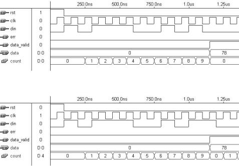
9.6 Serial Data Receiver
The diagram of a serial data receiver is shown in figure 9.13. It contains a serial data input, din, and a parallel data output, data(6:0). A clock signal is also needed at the input. Two supervision signals are generated by the circuit: err (error) and data_valid.
The input train consists of ten bits. The first bit is a start bit, which, when high, must cause the circuit to start receiving data. The next seven are the actual data bits. The ninth bit is a parity bit, whose status must be ‘0’ if the number of ones in data is even, or ‘1’ otherwise. Finally, the tenth is a stop bit, which must be high if the transmission is correct. An error is detected when either the parity does not check or the stop bit is not a ‘1’. When reception is concluded and if no error has been detected, then the data stored in the internal registers (reg) is transferred to data(6:0) and the data_valid output is asserted.
A VHDL code for this circuit is presented below. A few variables were used: count, to determine the number of bits received; reg, which stores the data; and temp, to compute the error. Notice in line 37 that reg(0) ¼ din was used instead of reg(0) ¼ ‘0’, because we want the time slot immediately after the stop bit to be considered as possibly containing a start bit for the next input train.
data
start parity stop
din |
|
|
|
|
|
|
|
|
|
err |
|
|
|
|
|
reg |
|
|
|
||
|
|
|
|
|
|
|
|
|
data_valid |
|
clk |
|
|
|
|
|
|
|
|
|
|
|
|
|
|
|
|
|
|
|
||
|
|
data |
(0) |
(1) |
(2) |
(3) |
(4) |
(5) |
(6) |
|
|
|
|
||||||||
Figure 9.13 |
|
|
|
|
|
|
|
|
||
Serial data receiver.
TLFeBOOK
Additional Circuit Designs |
209 |
1 ---------------------------------------------
2LIBRARY ieee;
3 USE ieee.std_logic_1164.all;
4 ---------------------------------------------
5ENTITY receiver IS
6PORT ( din, clk, rst: IN BIT;
7 |
data: OUT BIT_VECTOR |
(6 DOWNTO 0); |
8 |
err, data_valid: OUT |
BIT); |
9 |
END receiver; |
|
10 |
--------------------------------------------- |
|
11 ARCHITECTURE rtl OF receiver IS
12BEGIN
13PROCESS (rst, clk)
14VARIABLE count: INTEGER RANGE 0 TO 10;
15VARIABLE reg: BIT_VECTOR (10 DOWNTO 0);
16VARIABLE temp : BIT;
17BEGIN
18IF (rst='1') THEN
19count:=0;
20reg := (reg'RANGE => '0');
21temp := '0';
22err <= '0';
23data_valid <= '0';
24ELSIF (clk'EVENT AND clk='1') THEN
25IF (reg(0)='0' AND din='1') THEN
26reg(0) := '1';
27ELSIF (reg(0)='1') THEN
28count := count + 1;
29IF (count < 10) THEN
30 |
reg(count) := din; |
|
31 |
ELSIF (count = 10) |
THEN |
32 |
temp := (reg(1) |
XOR reg(2) XOR reg(3) XOR |
33 |
reg(4) |
XOR reg(5) XOR reg(6) XOR |
34 |
reg(7) XOR reg(8)) OR NOT reg(9); |
|
35 |
err <= temp; |
|
36 |
count := 0; |
|
37 |
reg(0) := din; |
|
38 |
IF (temp = '0') |
THEN |
TLFeBOOK
210 |
Chapter 9 |
39 |
data_valid <= '1'; |
|
40 |
data |
<= reg(7 DOWNTO 1); |
41 |
END IF; |
|
42END IF;
43END IF;
44END IF;
45END PROCESS;
46END rtl;
47-------------------------------------------------
Simulation results are presented in figure 9.14. The input sequence is din ¼ {start ¼ 1, din ¼ 0111001, parity ¼ 0, stop ¼ 1}. As can be seen in the upper graph, no error was detected in this case, because the parity and stop bits are correct. Hence, after count reaches 9, the data is made available, that is, data ¼ 0111001, from data(0) to data(6), which corresponds to the decimal 78, and the data_valid bit is
Figure 9.14
Simulation results of serial data receivers.
TLFeBOOK

Additional Circuit Designs |
211 |
asserted. Notice that the output remains so indefinitely, unless a new input train is received.
The only di¤erence in the lower graph is that a start bit appears immediately after the stop bit. As can be seen, the count variable starts then to count and the whole process is repeated.
9.7Parallel-to-Serial Converter
A parallel-to-serial converter is a typical application of shift registers. It consists of sending out a block of data serially. The need for such converters arises, for example, in ASIC chips when there are not enough pins available to output all data bits simultaneously.
A diagram of a parallel-to-serial converter is presented in figure 9.15. d(7:0) is the data vector to be sent out, while dout is the actual output. There are also two other inputs: clk and load. When load is asserted, d is synchronously stored in the shift register reg. While load stays high, the MSB, d(7), remains available at the output. Once load is returned to ‘0’, the subsequent bits are presented at the output at each positive edge of clk. After all eight bits have been sent out, the output remains low until the next transmission.
1 -------------------------------------------------
2LIBRARY ieee;
3 USE ieee.std_logic_1164.all;
4 -------------------------------------------------
5ENTITY serial_converter IS
6PORT ( d: IN STD_LOGIC_VECTOR (7 DOWNTO 0);
7 |
|
|
clk, load: IN STD_LOGIC; |
||||
8 |
|
|
dout: OUT STD_LOGIC); |
||||
9 |
END serial_converter; |
|
|
||||
10 ------------------------------------------------- |
|
|
|
|
|
|
|
|
d(0) d(1) d(2) d(3) d(4) d(5) |
d(6) d(7) |
|||||
|
|
|
|
|
|
|
|
|
|
|
|
|
|
|
|
|
|
|
|
|
|
|
|
clk |
|
|
|
|
|
|
dout |
|
|
|
|
|
|
||
|
|
|
reg |
|
|
||
load |
|
|
|
|
|
||
|
|
|
|
|
|
|
|
Figure 9.15 |
|
|
|||||
Parallel-to-serial converter. |
|
|
|||||
TLFeBOOK

212 |
Chapter 9 |
Figure 9.16
Simulation results of parallel-to-serial converter.
11 ARCHITECTURE serial_converter OF serial_converter IS
12SIGNAL reg: STD_LOGIC_VECTOR (7 DOWNTO 0);
13BEGIN
14PROCESS (clk)
15BEGIN
16IF (clk'EVENT AND clk='1') THEN
17IF (load='1') THEN reg <= d;
18ELSE reg <= reg(6 DOWNTO 0) & '0';
19END IF;
20END IF;
21END PROCESS;
22dout <= reg(7);
23END serial_converter;
24-------------------------------------------------
Simulation results from the circuit synthesized with the code above are shown in figure 9.16. d ¼ ‘‘11011011’’ (decimal 219) was chosen. As can be seen, d(7) ¼ ‘1’ is presented at the output at the first rising edge of clk after load has been asserted, staying there while load remains high (to illustrate this fact, load was kept high during two clock cycles). The other bits follow as soon as load returns to ‘0’. Notice that after all bits have been transmitted, the output stays low.
9.8 Playing with a Seven-Segment Display
We want to design a little game with an SSD (seven-segment display). The top-level diagram of the circuit is shown in figure 9.17. It contains two inputs, clk and stop, and one output, dout(6:0), which feeds the SSD. Assume that fclk ¼ 1 kHz.
TLFeBOOK
Additional Circuit Designs |
213 |
|
|
|
|
|
|
|
|
|
|
|
|
|
|
SSD |
|
|
|
|
|
|
|
|
|
|
|
|
|
|
|
|
|
|
a |
|
|
|
|
clk |
|
|
|
|
|
|
|
|
|
f |
|
|
|
b |
||||
|
|
|
|
|
|
|
|
|
|
|
|
|||||||
|
|
|
|
|
|
|
|
|
|
|
|
|
|
|
|
|||
|
|
|
|
|
|
|
|
|
|
|
|
|
|
|
|
|||
|
Little |
|
|
|
|
|
|
|
e |
|
g |
|
c |
|||||
|
|
|
|
|
|
|
|
|
|
|||||||||
|
|
|
|
|
|
|
|
|
|
|
|
|
||||||
|
|
|
|
|
|
|
|
|
|
|
|
|
|
|||||
|
|
|
|
game |
|
|
|
|
|
|
|
|
|
|
|
|
|
|
stop |
|
|
|
|
|
|
|
|
|
|
|
|
d |
|
|
x |
||
|
|
|
|
|
|
|
|
|
|
|
|
|
|
|
||||
|
|
|
|
|
dout (6:0) |
|
|
|||||||||||
|
|
|
|
|
|
|
|
|
|
|
|
|||||||
|
|
|
|
|
|
|
|
|
|
|
|
|
||||||
|
|
|
|
|
|
Input: “xabcdefg” |
||||||||||||
|
|
|
|
|
|
|
|
|
|
|
|
|||||||
Figure 9.17 |
|
|
|
|
|
|||||||||||||
|
|
|
|
|
|
|
|
|
|
|
|
|
||||||
Playing with an SSD. |
|
|
|
|
|
|
|
|
|
|
|
|
|
|||||
Our circuit should cause a continuous clockwise movement of the SSD segments. Also, in order to make the circulatory movement more realistic, we want to momentarily overlap neighboring segments. Consequently, the sequence should be a ! ab ! b ! bc ! c ! cd ! d ! de ! e ! ef ! f ! fa ! a, with the combined states (ab, bc, etc.) lasting only a few milliseconds. If stop is asserted, then the circuit should return to state a and remain so until stop is turned low again.
From chapter 8, it is clear that this is a circuit for which the FSM approach is appropriate. The states diagram is presented in figure 9.18. We want the system to remain in states a, b, c, etc. for time1 ¼ 80 ms, and in the combined states, ab, bc, etc., for time2 ¼ 30 ms. Therefore, a counter counting up to 80 (the clock period is 1 ms) or up to 30 can be employed to determine when to move to the next state.
A VHDL solution is shown below. Notice that it is a straight implementation of the FSM template seen in section 8.2. In lines 11–12, time1 and time2 were declared as two constants. Small values (4 and 2, respectively) were here used in order for the simulation results to fit well in one plot, but 80 and 30, respectively, were used in the actual physical implementation. A signal called flip was used to switch from time1 to time2, and vice-versa. Notice that the corresponding decimals are marked beside each value of dout, so they can be easily verified in the simulation results.
1 --------------------------------------------------------
2LIBRARY ieee;
3 USE ieee.std_logic_1164.all;
4 --------------------------------------------------------
5ENTITY ssd_game2 IS
6 PORT ( clk, stop: IN BIT;
TLFeBOOK
214
time1
time2
b
ab
time1
a
stop
time2
fa
f
time1
time2
Figure 9.18
States diagram for the circuit of figure 9.17.
Chapter 9
|
time2 |
|
bc |
c |
time1 |
|
|
cd
time2
d
time1
de
e
ef |
time2 |
time1
7 |
dout: OUT BIT_VECTOR (6 DOWNTO 0)); |
8 |
END ssd_game2; |
9 |
-------------------------------------------------------- |
10 ARCHITECTURE fsm OF ssd_game2 IS
11CONSTANT time1: INTEGER := 4; -- actual value is 80
12CONSTANT time2: INTEGER := 2; -- actual value is 30
13TYPE states IS (a, ab, b, bc, c, cd, d, de, e, ef, f, fa);
14SIGNAL present_state, next_state: STATES;
15SIGNAL count: INTEGER RANGE 0 TO 5;
16SIGNAL flip: BIT;
17BEGIN
18------- Lower section of FSM (Sec. 8.2): ------------
19PROCESS (clk, stop)
20BEGIN
21IF (stop='1') THEN
22present_state <= a;
23ELSIF (clk'EVENT AND clk='1') THEN
24IF ((flip='1' AND count=time1) OR
25(flip='0' AND count=time2)) THEN
26count <= 0;
TLFeBOOK
Additional Circuit Designs |
215 |
27present_state <= next_state;
28ELSE count <= count + 1;
29END IF;
30END IF;
31END PROCESS;
32------- Upper section of FSM (Sec. 8.2): ------------
33PROCESS (present_state)
34BEGIN
35CASE present_state IS
36WHEN a =>
37dout <= "1000000"; -- Decimal 64
38flip<='1';
39next_state <= ab;
40WHEN ab =>
41dout <= "1100000"; -- Decimal 96
42flip<='0';
43next_state <= b;
44WHEN b =>
45dout <= "0100000"; -- Decimal 32
46flip<='1';
47next_state <= bc;
48WHEN bc =>
49dout <= "0110000"; -- Decimal 48
50flip<='0';
51next_state <= c;
52WHEN c =>
53dout <= "0010000"; -- Decimal 16
54flip<='1';
55next_state <= cd;
56WHEN cd =>
57dout <= "0011000"; -- Decimal 24
58flip<='0';
59next_state <= d;
60WHEN d =>
61dout <= "0001000"; -- Decimal 8
62flip<='1';
63next_state <= de;
TLFeBOOK

216 |
Chapter 9 |
64WHEN de =>
65dout <= "0001100"; -- Decimal 12
66flip<='0';
67next_state <= e;
68WHEN e =>
69dout <= "0000100"; -- Decimal 4
70flip<='1';
71next_state <= ef;
72WHEN ef =>
73dout <= "0000110"; -- Decimal 6
74flip<='0';
75next_state <= f;
76WHEN f =>
77dout <= "0000010"; -- Decimal 2
78flip<='1';
79next_state <= fa;
80WHEN fa =>
81dout <= "1000010"; -- Decimal 66
82flip<='0';
83next_state <= a;
84END CASE;
85END PROCESS;
86END fsm;
87--------------------------------------------------------
Simulation results are presented in figure 9.19. As can be seen, the system stays in the single states, a, b, etc., for four clock cycles (time1 ¼ 4 here) and in the combined states, ab, bc, etc., for two clock cycles (time2 ¼ 2). Observe also that the decimals detected by the simulator match the decimals listed in the VHDL code.
Figure 9.19
Simulation results of little SSD game of figure 9.17.
TLFeBOOK

Additional Circuit Designs |
217 |
9.9Signal Generators
Say that, from a clock signal (clk), we want to obtain the waveform shown in figure 9.20. In this kind of problem, we can use either the FSM approach or a conventional approach. Both kinds of solutions are illustrated below.
FSM Approach
The signal of figure 9.20 can be modeled as an 8-state FSM. Using a counter from 0 to 7, we can establish that wave ¼ ‘0’ (1st pulse) when count ¼ 0, wave ¼ ‘1’ (2nd pulse) when count ¼ 1, and so on, thus creating the signal shown in the figure. This implementation requires a total of four flip-flops: three to store count (three bits), plus one to store wave (one bit). Recall from chapter 8, sections 8.2–8.3, that the output of a FSM will only be registered if design style #2 is employed, which is necessary here, because glitches are not acceptable in a signal generator.
The corresponding VHDL code, using dsign style #2 (section 8.3), is shown below. Simulation results appear in figure 9.21. Checking the report file created by the synthesis tool, we verify that a total of four flip-flops were indeed inferred from this code.
1 -----------------------------------------------------
2LIBRARY ieee;
3USE ieee.std_logic_1164.all;
clk
wave
1 period
Figure 9.20
Signal generator problem.
Figure 9.21
Simulation results of signal generator (FSM approach).
TLFeBOOK
218 |
Chapter 9 |
4 -----------------------------------------------------
5ENTITY signal_gen IS
6PORT (clk: IN STD_LOGIC;
7 |
wave: OUT STD_LOGIC); |
8 |
END signal_gen; |
9 |
----------------------------------------------------- |
10 |
ARCHITECTURE fsm OF signal_gen IS |
11 |
TYPE states IS (zero, one, two, three, four, five, six, |
12 |
seven); |
13SIGNAL present_state, next_state: STATES;
14SIGNAL temp: STD_LOGIC;
15BEGIN
16
17--- Lower section of FSM (Sec. 8.3): ---
18PROCESS (clk)
19BEGIN
20IF (clk'EVENT AND clk='1') THEN
21present_state <= next_state;
22wave <= temp;
23END IF;
24END PROCESS;
25
26--- Upper section of FSM (Sec. 8.3): ---
27PROCESS (present_state)
28BEGIN
29CASE present_state IS
30WHEN zero => temp<='0'; next_state <= one;
31WHEN one => temp<='1'; next_state <= two;
32WHEN two => temp<='0'; next_state <= three;
33WHEN three => temp<='1'; next_state <= four;
34WHEN four => temp<='1'; next_state <= five;
35WHEN five => temp<='1'; next_state <= six;
36WHEN six => temp<='0'; next_state <= seven;
37WHEN seven => temp<='0'; next_state <= zero;
38END CASE;
39END PROCESS;
40END fsm;
41 -----------------------------------------------------
TLFeBOOK
Additional Circuit Designs |
219 |
Figure 9.22
Simulation results of signal generator (conventional approach).
Conventional Approach
A conventional design, with the IF statement, is shown next. Notice that count and wave are both assigned at the transition of another signal (clk). Therefore, according to what you saw in section 7.5, both will be stored (that is, four flip-flops will be inferred, three for count and one for wave). Simulation results are shown in figure 9.22.
1 ---------------------------------------
2LIBRARY ieee;
3 USE ieee.std_logic_1164.all;
4 ---------------------------------------
5 ENTITY signal_gen1 IS
6 PORT (clk: IN BIT;
7 wave: OUT BIT);
8 END signal_gen1;
9 ---------------------------------------
10 ARCHITECTURE arch1 OF signal_gen1 IS
11BEGIN
12PROCESS
13VARIABLE count: INTEGER RANGE 0 TO 7;
14BEGIN
15WAIT UNTIL (clk'EVENT AND clk='1');
16CASE count IS
17WHEN 0 => wave <= '0';
18WHEN 1 => wave <= '1';
19WHEN 2 => wave <= '0';
20WHEN 3 => wave <= '1';
21WHEN 4 => wave <= '1';
22WHEN 5 => wave <= '1';
23WHEN 6 => wave <= '0';
TLFeBOOK

220 |
Chapter 9 |
ROM
word 0
addr |
|
|
|
word 1 |
|
|
|
data |
|
|
|||||||
|
|
|
||||||
|
|
|
|
word 2 |
|
|
|
|
|
|
|
|
|
|
|
|
|
|
|
|
|
… |
|
|
|
|
Figure 9.23
ROM diagram.
24WHEN 7 => wave <= '0';
25END CASE;
26count := count + 1;
27END PROCESS;
28END arch1;
29---------------------------------------
9.10 Memory Design
In this section, the design of the following memory circuits is presented:
ROM
RAM with separate in/out data buses
RAM with bidirectional in/out data bus
ROM (Read Only Memory)
Figure 9.23 shows the diagram of a ROM. Since it is a read-only memory, no clock signal or write-enable pin is necessary. As can be seen, the circuit contains a pile of pre-stored words, being the one selected by the address input (addr) presented at the output (data).
In the code shown below, words (line 7) represents the number of words stored in the memory, while bits (line 6) represents the size of each word. To create a ROM, an array of CONSTANT values can be used (lines 15–22). First, a new TYPE, called vector_array, was defined (lines 13–14), which was then used in the declaration of a CONSTANT named memory (line 15). An 8 8 ROM is illustrated in this example, with the following (decimal) values stored in addresses 0 to 7: 0, 2, 4, 8, 16, 32, 64, and 128 (lines 15–22). Line 24 shows an example of call to the memory; the output (data) is equal to the word stored at address addr. When implementing a ROM, no
TLFeBOOK
Additional Circuit Designs |
221 |
registers are inferred, because no signal assignment occurs at the transition of another signal. Logical gates, forming an LUT (lookup table), are used instead.
1 ---------------------------------------------------
2LIBRARY ieee;
3 USE ieee.std_logic_1164.all;
4 ---------------------------------------------------
5ENTITY rom IS
6 |
GENERIC ( bits: INTEGER := 8; |
-- |
# |
of |
bits per |
word |
7 |
words: INTEGER := 8); |
-- |
# |
of |
words in |
the memory |
8PORT ( addr: IN INTEGER RANGE 0 TO words-1;
9 |
data: OUT STD_LOGIC_VECTOR (bits-1 DOWNTO 0)); |
10 |
END rom; |
11 |
--------------------------------------------------- |
12 |
ARCHITECTURE rom OF rom IS |
13TYPE vector_array IS ARRAY (0 TO words-1) OF
14STD_LOGIC_VECTOR (bits-1 DOWNTO 0);
15CONSTANT memory: vector_array := ( "00000000",
16 |
"00000010", |
17 |
"00000100", |
18 |
"00001000", |
19 |
"00010000", |
20 |
"00100000", |
21 |
"01000000", |
22 |
"10000000"); |
23BEGIN
24data <= memory(addr);
25END rom;
26 ---------------------------------------------------
Simulation results are shown in figure 9.24. As can be seen, the address changes from 0 to 7, then restarts from 0, with the outputs matching the values listed in the code above.
RAM with Separate Input and Output Data Buses
A RAM (Random Access Memory), with separate input and output data buses, is illustrated in figure 9.25. Indeed, this circuit was already discussed in example 6.11, but was repeated here to ease the comparison with the other memory circuits presented in this section.
TLFeBOOK

222 |
Chapter 9 |
Figure 9.24
Simulation results from the 8 8 ROM code shown above.
|
|
|
|
|
RAM |
|
|
|
|
|
|
|
|
wr_ena |
|||||||
|
|
|
|
|
|
|
|
|
|
|
|
|
|
|
|
|
|
|
|||
|
|
|
|
|
|
|
|
|
|
|
|
|
|
|
|
||||||
data_in |
|
|
|
|
word 0 |
|
|
|
data_out |
|
wr_ena |
|
|
|
|
|
|
|
|||
|
|
|
|
|
|
||||||||||||||||
|
|
|
|
|
|
|
|
|
|
|
|
|
|
|
|
||||||
|
|
|
|
word 1 |
|
|
|
d |
|
|
|
|
|
|
|
|
|
|
q |
||
|
|
|
|
|
|
|
|
|
|
|
|
|
|
|
|
|
|
|
|
||
addr |
|
|
|
|
word 2 |
|
|
|
|
|
|
|
|
|
|
DFF |
|
|
|
||
|
|
|
|
|
|
|
|
|
|
|
|
|
|
|
|
|
|
|
|
|
|
|
|
|
|
… |
|
|
|
|
|
|
|
clk |
|
|
|
|
|
|
|
||
|
|
|
|
|
|
|
|
|
|
|
|
|
|
|
|
|
|
||||
|
|
|
|
|
|
|
|
|
|
|
|
|
|
|
|
|
|
|
|||
|
|
|
|
|
|
|
|
|
|
|
|
|
|
|
|
|
|
|
|||
|
|
|
|
|
|
|
|
|
|
|
|
|
|
|
|
|
|
|
|
|
|
|
|
|
|
|
|
|
|
|
|
|
|
|
|
|
|
|
|
|
|
|
|
clk wr_ena
(a) |
(b) |
Figure 9.25 |
|
RAM with separate in/out data buses. |
|
As can be seen in figure 9.25(a), the circuit has a data input bus (data_in), a data output bus (data_out), an address bus (addr), plus clock (clk) and write enable (wr_ena) pins. When wr_enable is asserted, at the next rising edge of clk the vector present at data_in must be stored in the position specified by addr. data_out, on the other hand, must constantly display the data selected by addr.
From the register point-of-view, the circuit can be summarized as in figure 9.25(b). When wr_ena is low, q is connected to the input of the flip-flop, and terminal d is open, so no new data will be written into the memory. However, when wr_ena is turned high, d is connected to the input of the register, so at the next rising edge of clk d will be stored.
A VHDL code that implements the circuit of figure 9.25 is shown below. The chosen capacity was 16 words of length eight bits each. Notice that the code is totally generic. Simulation results are shown in figure 9.26.
1 ---------------------------------------------------
2 LIBRARY ieee;
TLFeBOOK
Additional Circuit Designs |
223 |
Figure 9.26
Simulation results of 16 8 RAM with separate in/out data buses.
3 USE ieee.std_logic_1164.all;
4 ---------------------------------------------------
5ENTITY ram IS
6 |
GENERIC ( bits: INTEGER := 8; |
-- # |
of |
bits per word |
|
7 |
words: INTEGER := 16); |
-- |
# |
of |
words in the |
8 |
|
-- |
memory |
||
9PORT ( wr_ena, clk: IN STD_LOGIC;
10addr: IN INTEGER RANGE 0 TO words-1;
11data_in: IN STD_LOGIC_VECTOR (bits-1 DOWNTO 0);
12data_out: OUT STD_LOGIC_VECTOR (bits-1 DOWNTO 0));
13END ram;
14 ---------------------------------------------------
15 ARCHITECTURE ram OF ram IS
16TYPE vector_array IS ARRAY (0 TO words-1) OF
17STD_LOGIC_VECTOR (bits-1 DOWNTO 0);
18SIGNAL memory: vector_array;
19BEGIN
20PROCESS (clk, wr_ena)
21BEGIN
22IF (wr_ena='1') THEN
23IF (clk'EVENT AND clk='1') THEN
24memory(addr) <= data_in;
25END IF;
26END IF;
27END PROCESS;
28data_out <= memory(addr);
29END ram;
30 ---------------------------------------------------
TLFeBOOK

224 |
Chapter 9 |
|
|
|
|
|
RAM |
|
|
|
|
|
|
|
|
|
|
|
|
|
|
|
|
||
|
|
|
|
|
|
|
|
|
|
|
|
|
|
wr_ena |
|
|
|||||||
|
|
|
|
|
|
|
|
|
|
|
|
|
|
|
|
|
|
|
|||||
|
|
|
|
|
word 0 |
|
|
|
|||||||||||||||
addr |
|
|
|
|
|
|
bidir |
|
(d) |
|
|
|
|
|
|
|
|||||||
|
|
|
|
|
|
|
|
|
|
|
|
|
|
||||||||||
|
|
|
|
|
|
|
|||||||||||||||||
|
|
|
|
word 1 |
|
|
q |
||||||||||||||||
|
|
|
|
|
|
|
|
|
|
|
|
|
|
|
|
|
|
|
|
||||
|
|
|
|
|
|
|
|
|
|
|
|
|
|
|
|
|
|
|
|||||
|
|
|
|
|
|
|
|
|
|
|
|
|
|
|
|
|
|
||||||
|
|
|
|
|
|
|
|
|
|
|
|
|
|
|
|
|
|
|
|
|
|
|
|
|
|
|
|
|
word 2 |
|
|
|
|
|
|
|
|
DFF |
|
|
|
|
|
|
|
|
|
|
|
|
|
|
|
|
|
|
|
|
|
|
|
|
|
|
|
|
|
|
|
||
|
|
|
|
|
|
|
|
|
|
|
|
|
|
|
|
|
|
|
|
|
|
|
|
|
|
|
|
|
… |
|
|
|
clk |
|
|
|
|
|
|
|
|
|
|
|
|
||
|
|
|
|
|
|
|
|
|
|
|
|
|
|
|
|
|
|
|
|
||||
|
|
|
|
|
|
|
|
|
|
||||||||||||||
|
|
|
|
|
|
|
|
|
|
|
|
|
|
|
|
|
|
|
|
|
|
|
|
clk wr_ena
(a) |
(b) |
Figure 9.27
RAM with bidirectional in/out data bus.
Figure 9.28
Simulation results of 16 8 RAM with bidirectional in/out data bus.
RAM with Bidirectional In/Out Data Bus
A RAM with bidirectional in/out data bus is illustrated in figure 9.27. The overall structure is similar to that of figure 9.25, except for the fact that now the same bus (bidir) is used to write data into the memory as well to read data from it.
From the register point-of-view, the circuit can be summarized as in figure 9.27(b). When wr_ena is low, the output of the register is connected to its input, so no change on the store data will occur. On the other hand, when wr_ena is asserted, q is connected to d, allowing new data to be stored at the next rising edge of clk.
A VHDL code that implements the circuit of figure 9.27 is shown below. The chosen capacity was 16 words of length eight bits each. Notice that this code is also totally generic. Simulation results are shown in figure 9.28.
TLFeBOOK
Additional Circuit Designs |
225 |
1 -------------------------------------------------
2LIBRARY ieee;
3 USE ieee.std_logic_1164.all;
4 -------------------------------------------------
5ENTITY ram4 IS
6 |
GENERIC ( bits: INTEGER := 8; |
-- # |
of |
bits per word |
|
7 |
words: INTEGER := 16); |
-- |
# |
of |
words in the |
8 |
|
-- |
memory |
||
9PORT ( clk, wr_ena: IN STD_LOGIC;
10addr: IN INTEGER RANGE 0 TO words-1;
11bidir: INOUT STD_LOGIC_VECTOR (bits-1 DOWNTO 0));
12END ram4;
13 -------------------------------------------------
14 ARCHITECTURE ram OF ram4 IS
15TYPE vector_array IS ARRAY (0 TO words-1) OF
16STD_LOGIC_VECTOR (bits-1 DOWNTO 0);
17SIGNAL memory: vector_array;
18BEGIN
19PROCESS (clk, wr_ena)
20BEGIN
21IF (wr_ena='0') THEN
22bidir <= memory(addr);
23ELSE
24bidir <= (OTHERS => 'Z');
25IF (clk'EVENT AND clk='1') THEN
26memory(addr) <= bidir;
27END IF;
28END IF;
29END PROCESS;
30END ram;
31 -------------------------------------------------
9.11Problems
Problem 9.1: Barrel Shifter
Why can we not replace the ARCHITECTURE of the barrel shifter presented in section 9.1 by that shown below, which is much shorter?
TLFeBOOK
226 |
Chapter 9 |
---------------------------------------------
ARCHITECTURE barrel OF barrel IS
BEGIN
PROCESS (inp, shift)
BEGIN
IF (shift=0) THEN
outp <= inp;
ELSE
FOR i IN 0 TO shift-1 LOOP outp(i) <= '0';
END LOOP;
FOR i IN shift TO inp'HIGH LOOP outp(i) <= inp(i-1);
END LOOP;
END IF;
END PROCESS;
END barrel;
---------------------------------------------
Problem 9.2: Divider
In section 9.4, we studied the design of fixed-point dividers. Two solutions were presented, both using sequential statements (IF and LOOP). Moreover, the codes implemented the second description of the division algorithm presented in that section. You are asked to write a concurrent solution for the division problem (with GENERATE). Additionally, your code should resemble the first description of the division algorithm (figure 9.9). In order to do so, we suggest the creation and use of the following types and signal:
SUBTYPE long IS STD_LOGIC_VECTOR (2n DOWNTO 0);
TYPE vec_array IS ARRAY (n DOWNTO 0) OF long;
SIGNAL a_input, b_input: vec_array;
where n should be declared as a GENERIC parameter.
Problem 9.3: Vending-Machine Controller
Consider the vending-machine controller designed in section 9.5. We want to introduce some sophistications in it.
TLFeBOOK

Additional Circuit Designs |
227 |
(a) In order to provide the necessary security, introduce some kind of handshake between the controller and the external circuitry. As an example, the handshake could include the following:
(i)an ‘‘input valid’’ signal (call it coin_valid), from the external circuit to the controller, informing that a new input is ready to be read. This signal should return to ‘0’ as soon as it has been processed by the controller, so a new input will only be considered by the controller at its rising edge. This is important to avoid possible confusion which may occur when nickel_in, dime_in, or quarter_in stays present at the input of the FSM for more than one clock cycle (so it will not be interpreted as a second coin, as in the design of section 9.5)
(ii)an ‘‘input accepted’’ signal (call it coin_accepted), from the controller to the external circuit, informing that the present input has already been processed. Upon receiving this signal, the external circuit should cause coin_valid to return to ‘0’.
(b)Consider that the nickel or the dime box in the vending machine might run out of coins. Design alternative return paths taking such possibilities into consideration. (Suggestion: simply include new arrows between st45 ! st40 and st35 ! st30 in the FSM diagram of figure 9.11).
(c)Finally, consider the situation where a customer might continue depositing coins even when the necessary amount has already been reached. What should be done in such a situation?
Problem 9.4: Serial Data Receiver
Try to model and design the serial data receiver of section 9.6 utilizing the FSM (finite state machine) approach (chapter 8). Before you start writing you VHDL code, present a clear states diagram of the system.
Problem 9.5: Serial Data Transmitter
This problem is the counterpart of that treated in section 9.6. Here, the stored data must be transmitted serially. A diagram of the circuit is shown in figure P9.5. The
data in
start |
|
|
|
|
|
|
parity stop |
data_ready |
|
|
|
|
|
|
|
‘1’ (0) (1) (2) (3) (4) (5) (6) p ‘1’ |
|
dout |
|
clk |
|
|
|
||
|
|
|
|
|
|
Figure P9.5 |
|
||||
TLFeBOOK
228 |
Chapter 9 |
protocol is the same 10-bit structure of section 9.6; that is, a start bit (high), followed by seven bits of actual data, plus a parity bit, computed such that the total number of ‘1’s in positions 2 to 9 is even, and finally a stop bit (also ‘1’). Consider that a data_ready signal is available to inform when the data can be loaded into the registers and sent out.
Problem 9.6: Playing with an SSD
You are asked to introduce additional features in the little seven-segment display (SSD) game of section 9.8.
(a)Add a 2-bit input, called ‘‘speed’’, which should be able to select four di¤erent speeds for the circulatory movement. Keep the overlap time (time2) fixed at 30 ms, changing only time1. Choose four di¤erent circulatory periods and physically verify whether the circuit behaves as expected.
(b)Change the functionality of the stop input, such that instead of going to state when a stop is asserted, it freezes in whatever state it was when stop was activated, proceeding from there when stop returns to zero.
(c)Finally, add a ‘‘direction’’ pin. When low, the circuit should behave as above, but when high, it should circulate in the opposite direction (counterclockwise).
(d)Physical verification: After synthesizing and simulating your design, physically implement it in you PLD/FPGA development kit, following the steps below.
(i)First, verify in the report file generated by the compiler which pins of the chip were assigned to the inputs (clock and switches) and to the outputs (SSD).
(ii)Next, connect the signal generator (set to 1 kHz, with the appropriate logic levels, but leave it OFF while you make the connection) and the switches (which should provide VDD and GND levels) to the inputs of the circuit (your development kit board is normally equipped with test switches).
(iii)Connect the outputs of the chip to the SSD (your development kit board is normally equipped with seven-segment displays).
(iv)Finally, download the compiled file from your computer to the development kit, turn ON the signal generator, and verify the operation of your circuit. Play with the switches in order to test all operation modes.
Problem 9.7: Speed Monitor
Figure P9.7 shows a possible view of a car speed monitor. The specifications of the system are the following:
TLFeBOOK
Additional Circuit Designs |
229 |
|||
|
|
|
|
|
|
|
|
|
|
ON/OFF
SPEED
35 45 55 60 65 70 75 80
Figure P9.7
Speed selection button (SPEED), which, at each touch, selects the next speed to be monitored (35, 45, 55, 60, 65, 70, 75, or 80 miles/hour).
Set of eight LEDs, one for each speed. The LED corresponding to the selected speed should be ON.
Two SSDs, which show the actual speed of the car. The car’s electronic speedometer provides a clock signal whose frequency is proportional to the speed. You may check the data sheet of the speedometer that you are going to use, or you can start with a simple round number, which you can provide with a signal generator to test your circuit (say, 100 Hz per mile/hour).
Buzzer, which emits alarm signals as the car approaches the selected speed. A 2 Hz signal should be emitted when the speed is three miles/hour or less from the selected speed, or a continuous alarm when at or above the selected speed. Consider a buzzer with internal oscillator, so only a DC signal must be provided in the latter case, or a square wave with frequency 2 Hz in the former case.
Write a VHDL code for such a circuit. Synthesize and simulate it. Finally, physically implement it in your PLD/FPGA development kit, using a signal generator for clock and following steps similar to those in problem 9.6.
Problem 9.8: Random Number Generator
Design a 1-digit random number generator. The number should be from ‘‘0000’’ (display ¼ 0) to ‘‘1111’’ (display ¼ F). Use the circuit of section 9.8, with a modified function for the stop switch. The SSD should remain in a circular motion until the switch is pressed. When pressed, a random number should be displayed, being the circular movement resumed at the next touch of the switch. After compiling and simulating your circuit, physically implement it in your PDD/FPGA development kit.
TLFeBOOK
TLFeBOOK
II SYSTEM DESIGN
TLFeBOOK
TLFeBOOK
10 Packages and Components
10.1Introduction
In Part I of the book, we studied the entire background and coding techniques of VHDL, which included the following:
Code structure: library declarations, entity, architecture (chapter 2)
Data types (chapter 3)
Operators and attributes (chapter 4)
Concurrent statements and concurrent code (chapter 5)
Sequential statements and sequential code (chapter 6)
Signals, variables, and constants (chapter 7)
Design of finite state machines (chapter 8)
Additional circuit designs (chapter 9)
Thus, in terms of figure 10.1, we may say that we have covered in detail all that is needed to construct the type of code depicted on its left-hand side. A good understanding of that material is indispensable, regardless of the design being just a small circuit or a very large system.
In Part II, we will simply add new building blocks to the material already presented. These new building blocks are intended mainly for library allocation, being shown on the right-hand side of figure 10.1. They are:
Packages (chapter 10)
Components (chapter 10)
Functions (chapter 11)
Procedures (chapter 11)
These new units can be located in the main code itself (that is, on the left-hand side of figure 10.1). However, since their main purpose is to allow common pieces of code to be reused and shared, it is more usual to place them in a LIBRARY. This also leads to code partitioning, which is helpful when dealing with long codes. In summary, frequently used pieces of code can be written in the form of COMPONENTS, FUNCTIONS, or PROCEDURES, then placed in a PACKAGE, which is finally compiled into the destination LIBRARY.
We have already seen (chapter 2) that at least three LIBRARIES are generally needed in a design: ieee, std, and work. After studying Part II, we will be able to construct our own libraries, which can then be added to the list above.
TLFeBOOK

234 |
Chapter 10 |
Main code |
Library |
declarations |
ENTITY |
ARCHITECTURE |
Figure 10.1
Fundamental units of VHDL code.
10.2 PACKAGE
LIBRARY |
PACKAGE |
COMPONENT |
FUNCTION |
PROCEDURE |
As mentioned above, frequently used pieces of VHDL code are usually written in the form of COMPONENTS, FUNCTIONS, or PROCEDURES. Such codes are then placed inside a PACKAGE and compiled into the destination LIBRARY. The importance of this technique is that it allows code partitioning, code sharing, and code reuse.
We start by describing the structure of a PACKAGE. Besides COMPONENTS, FUNCTIONS, and PROCEDURES, it can also contain TYPE and CONSTANT definitions, among others. Its syntax is presented below.
PACKAGE package_name IS (declarations)
END package_name;
[PACKAGE BODY package_name IS
(FUNCTION and PROCEDURE descriptions) END package_name;]
As can be seen, the syntax is composed of two parts: PACKAGE and PACKAGE BODY. The first part is mandatory and contains all declarations, while the second
TLFeBOOK
Packages and Components |
235 |
part is necessary only when one or more subprograms (FUNCTION or PROCEDURE) are declared in the upper part, in which case it must contain the descriptions (bodies) of the subprograms. PACKAGE and PACKAGE BODY must have the same name.
The declarations list can contain the following: COMPONENT, FUNCTION, PROCEDURE, TYPE, CONSTANT, etc.
Example 10.1: Simple Package
The example below shows a PACKAGE called my_package. It contains only TYPE and CONSTANT declarations, so a PACKAGE BODY is not necessary.
1 ------------------------------------------------
2LIBRARY ieee;
3 USE ieee.std_logic_1164.all;
4 ------------------------------------------------
5PACKAGE my_package IS
6 TYPE state IS (st1, st2, st3, st4);
7TYPE color IS (red, green, blue);
8 CONSTANT vec: STD_LOGIC_VECTOR(7 DOWNTO 0) := "11111111"; 9 END my_package;
10 ------------------------------------------------
Example 10.2: Package with a Function
This example contains, besides TYPE and CONSTANT declarations, a FUNCTION. Therefore, a PACKAGE BODY is now needed (details on how to write a FUNCTION will be seen in chapter 11). This function returns TRUE when a positive edge occurs on clk.
1 -------------------------------------------------
2LIBRARY ieee;
3 |
USE ieee.std_logic_1164.all; |
4 |
------------------------------------------------- |
5PACKAGE my_package IS
6 TYPE state IS (st1, st2, st3, st4);
7TYPE color IS (red, green, blue);
8CONSTANT vec: STD_LOGIC_VECTOR(7 DOWNTO 0) := "11111111";
9 FUNCTION positive_edge(SIGNAL s: STD_LOGIC) RETURN BOOLEAN;
10 END my_package;
TLFeBOOK
236 |
Chapter 10 |
11 -------------------------------------------------
12 PACKAGE BODY my_package IS
13FUNCTION positive_edge(SIGNAL s: STD_LOGIC) RETURN BOOLEAN IS
14BEGIN
15RETURN (s'EVENT AND s='1');
16END positive_edge;
17END my_package;
18 -------------------------------------------------
Any of the PACKAGES above (example 10.1 or example 10.2) can now be compiled, becoming then part of our work LIBRARY (or any other). To make use of it in a VHDL code, we have to add a new USE clause to the main code (USE work.my_package.all), as shown below.
------------------------------------
LIBRARY ieee;
USE ieee.std_logic_1164.all;
USE work.my_package.all;
------------------------------------
ENTITY...
...
ARCHITECTURE...
...
------------------------------------
10.3 COMPONENT
A COMPONENT is simply a piece of conventional code (that is, LIBRARY declarations þ ENTITY þ ARCHITECTURE, as seen in chapter 2). However, by declaring such code as being a COMPONENT, it can then be used within another circuit, thus allowing the construction of hierarchical designs.
A COMPONENT is also another way of partitioning a code and providing code sharing and code reuse. For example, commonly used circuits, like flip-flops, multiplexers, adders, basic gates, etc., can be placed in a LIBRARY, so any project can make use of them without having to explicitly rewrite such codes.
To use (instantiate) a COMPONENT, it must first be declared. The corresponding syntaxes are shown below.
TLFeBOOK

Packages and Components |
237 |
COMPONENT declaration:
COMPONENT component_name IS PORT (
port_name : signal_mode signal_type; port_name : signal_mode signal_type;
...); END COMPONENT;
COMPONENT instantiation:
label: component_name PORT MAP (port_list);
As can be seen, the syntax of the declaration is similar to that of an ENTITY (section 2.3); that is, the names of the ports must be specified, along with their modes (IN, OUT, BUFFER, or INOUT) and data types (STD_LOGIC_VECTOR, INTEGER, BOOLEAN, etc.). To instantiate a component a label is required, followed by the component’s name and a PORT MAP declaration. Finally, port_list is just a list relating the ports of the actual circuit to the ports of the pre-designed component which is being instantiated.
Example: Let us consider an inverter, which has been previously designed (inverter.vhd) and compiled into the work library. We can make use of it by means of the code shown below. The label chosen for this component was U1. The names of the ports in the actual circuit are x and y, which are being assigned to a and b, respectively, of the pre-designed inverter (this is called positional mapping, for the first signal in one corresponds to the first signal in the other, the second in one to the second in the other, and so on).
-----COMPONENT declaration: -----------
COMPONENT inverter IS
PORT (a: IN STD_LOGIC; b: OUT STD_LOGIC); END COMPONENT;
-----COMPONENT instantiation: -----------
U1: inverter PORT MAP (x, y);
There are two basic ways to declare a COMPONENT (figure 10.2). Once we have designed it and placed it in the destination LIBRARY, we can declare it in the
TLFeBOOK
238 |
Chapter 10 |
main code itself, as shown in figure 10.2(a), or we can declare it using a PACKAGE, as in figure 10.2(b). The latter avoids the repetition of the declaration every time the COMPONENT is instantiated. Examples of both approaches are presented below.
Example 10.3: Components Declared in the Main Code
We want to implement the circuit of figure 10.3 employing only COMPONENTS (inverter, nand_2, and nand_3), but without creating a specific PACKAGE to declare them, thus as in figure 10.2(a). Then four pieces of VHDL code are needed: one for each component, plus one for the project (main code). All four files are shown below. Notice that, since we have not created a PACKAGE, the COMPONENTS must be declared in the main code (in the declarative part of the ARCHITECTURE). Simulation results are presented in figure 10.4.
1------ File inverter.vhd: -------------------
2 LIBRARY ieee;
3 USE ieee.std_logic_1164.all;
4 ------------------------------------
5 ENTITY inverter IS
6 PORT (a: IN STD_LOGIC; b: OUT STD_LOGIC); 7 END inverter;
8 ------------------------------------
9 ARCHITECTURE inverter OF inverter IS
10 BEGIN
11 b <= NOT a;
12 END inverter;
13 ---------------------------------------------
1------ File nand_2.vhd: ---------------------
2LIBRARY ieee;
3 USE ieee.std_logic_1164.all;
4 ------------------------------------
5ENTITY nand_2 IS
6 PORT (a, b: IN STD_LOGIC; c: OUT STD_LOGIC); 7 END nand_2;
8 ------------------------------------
9 ARCHITECTURE nand_2 OF nand_2 IS
TLFeBOOK
Packages and Components |
239 |
LIBRARY
COMPONENT |
Inverter |
COMPONENT
Nand_2
COMPONENT
Nand_3
Main code
Component
Declarations
-------------
Component
Instantiations
|
LIBRARY |
|
COMPONENT |
|
|
Inverter |
|
|
|
PACKAGE |
Main code |
|
|
|
COMPONENT |
|
|
Nand_2 |
Component |
Component |
|
Declarations |
Instantiations |
COMPONENT |
|
|
Nand_3 |
|
|
Figure 10.2
Basic ways of declaring COMPONENTS: (a) declarations in the main code itself, (b) declarations in a PACKAGE.
TLFeBOOK

240 |
Chapter 10 |
a
x
b
c |
y |
d |
|
Figure 10.3
Circuit of example 10.3.
10BEGIN
11c <= NOT (a AND b);
12END nand_2;
13 ---------------------------------------------
1----- File nand_3.vhd: ----------------------
2 LIBRARY ieee;
3 USE ieee.std_logic_1164.all;
4 ------------------------------------
5 ENTITY nand_3 IS
6 PORT (a, b, c: IN STD_LOGIC; d: OUT STD_LOGIC); 7 END nand_3;
8 ------------------------------------
9 ARCHITECTURE nand_3 OF nand_3 IS 10 BEGIN
11 d <= NOT (a AND b AND c);
12 END nand_3;
13 ---------------------------------------------
1----- File project.vhd: ---------------------
2LIBRARY ieee;
3 USE ieee.std_logic_1164.all;
4 ------------------------------------
5ENTITY project IS
6PORT (a, b, c, d: IN STD_LOGIC;
7 |
x, y: OUT STD_LOGIC); |
8 |
END project; |
9 |
------------------------------------ |
TLFeBOOK
Packages and Components |
241 |
10 ARCHITECTURE structural OF project IS
11 -------------
12COMPONENT inverter IS
13PORT (a: IN STD_LOGIC; b: OUT STD_LOGIC);
14END COMPONENT;
15 -------------
16COMPONENT nand_2 IS
17PORT (a, b: IN STD_LOGIC; c: OUT STD_LOGIC);
18END COMPONENT;
19 -------------
20COMPONENT nand_3 IS
21PORT (a, b, c: IN STD_LOGIC; d: OUT STD_LOGIC);
22END COMPONENT;
23 -------------
24SIGNAL w: STD_LOGIC;
25BEGIN
26U1: inverter PORT MAP (b, w);
27U2: nand_2 PORT MAP (a, b, x);
28U3: nand_3 PORT MAP (w, c, d, y);
29END structural;
30 ---------------------------------------------
Example 10.4: Components Declared in a Package
We want to implement the same project of the previous example (figure 10.3). However, we will now create a PACKAGE where all the COMPONENTS (inverter, nand_2, and nand_3) will be declared, like in figure 10.2(b). Thus now five pieces of VHDL code are needed: one for each component, one for the PACKAGE, and finally one for the project. Despite having an extra file (PACKAGE), such extra file needs to be created only once, thus avoiding the need to declare the components in the main code every time they are instantiated.
Notice that an extra USE clause (USE work.my_components.all) is now necessary, in order to make the PACKAGE my_components visible to the design. The simulation results are obviously the same as those of figure 10.4.
1 ------ File inverter.vhd: -------------------
2LIBRARY ieee;
3 USE ieee.std_logic_1164.all;
4 ------------------------------------
TLFeBOOK

242 |
Chapter 10 |
Figure 10.4
Experimental results of example 10.3.
5ENTITY inverter IS
6 PORT (a: IN STD_LOGIC; b: OUT STD_LOGIC); 7 END inverter;
8 ------------------------------------
9 ARCHITECTURE inverter OF inverter IS
10BEGIN
11b <= NOT a;
12END inverter;
13---------------------------------------------
1------ File nand_2.vhd: ---------------------
2 LIBRARY ieee;
3 USE ieee.std_logic_1164.all;
4 ------------------------------------
5 ENTITY nand_2 IS
6 PORT (a, b: IN STD_LOGIC; c: OUT STD_LOGIC); 7 END nand_2;
8 ------------------------------------
9 ARCHITECTURE nand_2 OF nand_2 IS 10 BEGIN
11 c <= NOT (a AND b);
12 END nand_2;
13 ---------------------------------------------
1----- File nand_3.vhd: ----------------------
2LIBRARY ieee;
3 USE ieee.std_logic_1164.all;
4 ------------------------------------
TLFeBOOK
Packages and Components |
243 |
5ENTITY nand_3 IS
6 PORT (a, b, c: IN STD_LOGIC; d: OUT STD_LOGIC); 7 END nand_3;
8 ------------------------------------
9 ARCHITECTURE nand_3 OF nand_3 IS
10BEGIN
11d <= NOT (a AND b AND c);
12END nand_3;
13 ---------------------------------------------
1 ----- File my_components.vhd: ---------------
2LIBRARY ieee;
3 USE ieee.std_logic_1164.all;
4 ------------------------
5PACKAGE my_components IS
6 ------ |
inverter: ------- |
7COMPONENT inverter IS
8 PORT (a: IN STD_LOGIC; b: OUT STD_LOGIC);
9END COMPONENT;
10------ 2-input nand: ---
11COMPONENT nand_2 IS
12PORT (a, b: IN STD_LOGIC; c: OUT STD_LOGIC);
13END COMPONENT;
14------ 3-input nand: ---
15COMPONENT nand_3 IS
16PORT (a, b, c: IN STD_LOGIC; d: OUT STD_LOGIC);
17END COMPONENT;
18 ------------------------
19 END my_components;
20 ---------------------------------------------
1 ----- File project.vhd: ---------------------
2LIBRARY ieee;
3 USE ieee.std_logic_1164.all;
4 USE work.my_components.all;
5 ---------------------------------
6ENTITY project IS
7PORT ( a, b, c, d: IN STD_LOGIC;
8 |
x, y: OUT STD_LOGIC); |
TLFeBOOK
244 |
Chapter 10 |
9END project;
10---------------------------------
11ARCHITECTURE structural OF project IS
12SIGNAL w: STD_LOGIC;
13BEGIN
14U1: inverter PORT MAP (b, w);
15U2: nand_2 PORT MAP (a, b, x);
16U3: nand_3 PORT MAP (w, c, d, y);
17END structural;
18---------------------------------------------
10.4 PORT MAP
There are two ways to map the PORTS of a COMPONENT during its instantiation: positional mapping and nominal mapping. Let us consider the following example:
COMPONENT inverter IS
PORT (a: IN STD_LOGIC; b: OUT STD_LOGIC);
END COMPONENT;
...
U1: inverter PORT MAP (x, y);
In it, the mapping is positional; that is, PORTS x and y correspond to a and b, respectively. On the other hand, a nominal mapping would be the following:
U1: inverter PORT MAP (x=>a, y=>b);
Positional mapping is easier to write, but nominal mapping is less error-prone. Ports can also be left unconnected (using the keyword OPEN). For example:
U2: my_circuit PORT MAP (x=>a, y=>b, w=>OPEN, z=>d);
10.5 GENERIC MAP
GENERIC units (discussed in section 4.5) can also be instantiated. In that case, a GENERIC MAP must be used in the COMPONENT instantiation to pass information to the GENERIC parameters. The new syntax is shown below.
TLFeBOOK

Packages and Components |
245 |
|
|
|
|
|
PARITY |
|
|
|
input (n-1:0) |
|
|
|
|
|
|
output (n:0) |
|
|
|
|
GENERATOR |
|
|
|||
|
|
|
|
|
|
|
|
|
|
|
|
|
|
|
|
|
|
Figure 10.5
Generic parity generator to be instantiated in example 10.5.
label: compon_name GENERIC MAP (param. list) PORT MAP (port list);
As can be seen, the only di¤erences from the syntax already presented are the inclusion of the word GENERIC and of a parameter list. The purpose is to inform that those parameters are to be considered as generic. The usage of GENERIC MAP is illustrated in the example below.
Example 10.5: Instantiating a Generic Component
Let us consider the generic parity generator of example 4.3 (repeated in figure 10.5), which adds one bit to the input vector (on its left-hand side). Such bit must be a ‘0’ if the number of ‘1’s in the input vector is even, or a ‘1’ if it is odd, such that the resulting vector will always contain an even number of ‘1’s.
The code presented below is generic (that is, works for any positive integer n). Two files are shown: one relative to the COMPONENT (par_generator, which, indeed, we can assume as previously designed and available in the work library), and one relative to the project itself (main code), where the component par_generator is instantiated.
Notice that the default value (n ¼ 7) of GENERIC in the COMPONENT file (parity_gen) will be overwritten by the value n ¼ 2 passed to it by means of the GENERIC MAP statement in the COMPONENT instantiation. Notice also that the GENERIC declaration that appears along with the COMPONENT declaration in the second file is necessary, for it is part of the original (the component’s) ENTITY. However, it is not necessary to declare its default value again. Simulation results from the circuit synthesized with the code below are shown in figure 10.6.
1 ------ File parity_gen.vhd (component): -------------
2LIBRARY ieee;
3USE ieee.std_logic_1164.all;
4-----------------------------------
TLFeBOOK

246 |
Chapter 10 |
Figure 10.6
Simulation results of example 10.5.
5ENTITY parity_gen IS
6 GENERIC (n : INTEGER := 7); -- default is 7
7PORT ( input: IN BIT_VECTOR (n DOWNTO 0);
8 |
output: OUT BIT_VECTOR (n+1 DOWNTO 0)); |
9 |
END parity_gen; |
10 |
----------------------------------- |
11 |
ARCHITECTURE parity OF parity_gen IS |
12BEGIN
13PROCESS (input)
14VARIABLE temp1: BIT;
15VARIABLE temp2: BIT_VECTOR (output'RANGE);
16BEGIN
17temp1 := '0';
18FOR i IN input'RANGE LOOP
19temp1 := temp1 XOR input(i);
20temp2(i) := input(i);
21END LOOP;
22temp2(output'HIGH) := temp1;
23output <= temp2;
24END PROCESS;
25END parity;
26 ------------------------------------------------------
1 ------ File my_code.vhd (actual project): ------------
2LIBRARY ieee;
3 USE ieee.std_logic_1164.all;
4 -----------------------------------
5ENTITY my_code IS
6 GENERIC (n : POSITIVE := 2); -- 2 will overwrite 7 7 PORT ( inp: IN BIT_VECTOR (n DOWNTO 0);
TLFeBOOK
Packages and Components |
247 |
8 |
outp: OUT BIT_VECTOR (n+1 DOWNTO 0)); |
|
9 |
END my_code; |
|
10 |
----------------------------------- |
|
11 |
ARCHITECTURE |
my_arch OF my_code IS |
12 |
------------------------ |
|
13COMPONENT parity_gen IS
14GENERIC (n : POSITIVE);
15PORT (input: IN BIT_VECTOR (n DOWNTO 0);
16output: OUT BIT_VECTOR (n+1 DOWNTO 0));
17END COMPONENT;
18 ------------------------
19BEGIN
20C1: parity_gen GENERIC MAP(n) PORT MAP(inp, outp);
21END my_arch;
22 ------------------------------------------------------
Example 10.6: ALU Made of COMPONENTS
In example 5.5, the design of an ALU (Arithmetic Logic Unit) was presented (diagram repeated in figure 10.7). In that example, the code was self-contained (that is, no external COMPONENT, FUNCTION, or PROCEDURE was called). In the present example, however, we will assume that our library contains the three components (logic_unit, arith_unit, and mux) with which the ALU can be constructed.
In the code shown below, besides the main code (alu.vhd), we have also included the design of the three components mentioned above. As can be seen, the COMPONENTS were declared in the main code itself. Simulation results are shown in figure 10.8, which are similar to those of example 5.5.
1 -------- |
COMPONENT arith_unit: -------------------- |
2LIBRARY ieee;
3USE ieee.std_logic_1164.all;
4 USE ieee.std_logic_unsigned.all;
5 -----------------------------------------
6ENTITY arith_unit IS
7PORT ( a, b: IN STD_LOGIC_VECTOR (7 DOWNTO 0);
8sel: IN STD_LOGIC_VECTOR (2 DOWNTO 0);
9cin: IN STD_LOGIC;
10x: OUT STD_LOGIC_VECTOR (7 DOWNTO 0));
11END arith_unit;
TLFeBOOK

248 Chapter 10
a (7:0) |
|
|
|
|
|
|
|
|
|
|
|
|
|
|
|
|
|
|
|
|
|
|
|
b (7:0) |
|
|
|
|
|
|
logic_unit |
|
|
|
|
|
|
|
|
|
|
|
|
|
|||
|
|
|
|
|
|
|
|
|
|
|
|
|
|
|
|
|
|
|
|||||
|
|
|
|
|
|
|
|
|
|
|
|
|
|
|
|
|
|
|
|
|
|
|
|
|
|
|
|
|
|
|
|
|
|
|
|
|
|
|
|
|
|
|
|
|
|
|
|
|
|
|
|
|
|
|
|
|
|
|
|
|
|
|
|
mux |
|
|
|
y (7:0) |
|
||
|
|
|
|
|
|
|
|
|
|
|
|
|
|
||||||||||
|
|
|
|
|
|
|
|
|
|
|
|
|
|
|
|
|
|
|
|
|
|
|
|
|
|
|
|
|
|
|
|
|
|
|
|
|
|
|
|
|
|
|
|
|
|
|
|
|
|
|
|
|
|
|
|
|
|
|
|
|
|
|
|
|
|
|
|
|
|
||
|
|
|
|
|
|
|
|
|
|
|
|
|
|
|
|
|
|
|
|
|
|
|
|
|
cin |
|
|
|
|
|
|
arith_unit |
|
|
|
|
|
|
sel (3) |
|
|||||||
|
|
|
|
|
|
|
|
|
|
|
|
|
|
|
|
|
|||||||
sel (3:0) |
|
|
|
|
|
|
|
|
|
|
|
|
|
|
|
|
|
|
|
|
|
|
|
|
|
|
|
|
|
|
|
|
|
|
|
|
|
|
|
|
|
|
|
|
|
||
|
|
|
|
|
|
|
|
|
|
|
|
|
|
|
|
|
|
|
|
|
|
||
|
|
|
|
|
|
|
|
|
|
|
|
|
|
|
|
|
|
|
|
|
|
|
|
|
sel |
Operation |
|
|
|
|
Function |
|
|
Unit |
|
||||||||||||
|
0000 |
|
y <= a |
|
|
|
|
Transfer a |
|
|
|
|
|
|
|||||||||
|
0001 |
|
y <= a+1 |
|
|
|
|
Increment a |
|
|
|
|
|
|
|||||||||
|
0010 |
|
y <= a-1 |
|
|
|
Decrement a |
|
|
|
|
|
|
||||||||||
|
0011 |
|
y <= b |
|
|
|
|
Transfer b |
|
Arithmetic |
|
||||||||||||
|
0100 |
|
y <= b+1 |
|
|
|
|
Increment b |
|
|
|
|
|
|
|||||||||
|
0101 |
|
y <= b-1 |
|
|
|
Decrement b |
|
|
|
|
|
|
||||||||||
|
0110 |
|
y <= a+b |
|
|
|
|
Add a and b |
|
|
|
|
|
|
|||||||||
|
0111 |
y <= a+b+cin |
|
Add a and b with carry |
|
|
|
|
|
|
|||||||||||||
|
1000 |
y <= NOT a |
|
|
Complement a |
|
|
|
|
|
|
||||||||||||
|
1001 |
y <= NOT b |
|
|
Complement b |
|
|
|
|
|
|
||||||||||||
|
1010 |
y <= a AND b |
|
|
|
|
AND |
|
|
|
|
|
|
||||||||||
|
1011 |
y <= a OR b |
|
|
|
|
OR |
|
|
Logic |
|
||||||||||||
|
1100 |
y <= a NAND b |
|
|
|
|
NAND |
|
|
|
|
|
|
||||||||||
|
1101 |
y <= a NOR b |
|
|
|
|
NOR |
|
|
|
|
|
|
||||||||||
|
1110 |
y <= a XOR b |
|
|
|
|
XOR |
|
|
|
|
|
|
||||||||||
|
1111 |
y <= a XNOR b |
|
|
|
|
XNOR |
|
|
|
|
|
|
||||||||||
Figure 10.7 |
|
|
|
|
|
|
|
|
|
|
|
|
|
|
|
|
|
|
|
|
|
|
|
ALU constructed from three COMPONENTS.
TLFeBOOK
Packages and Components |
249 |
Figure 10.8
Simulation results of example 10.6.
12 -----------------------------------------
13 ARCHITECTURE arith_unit OF arith_unit IS
14SIGNAL arith, logic: STD_LOGIC_VECTOR (7 DOWNTO 0);
15BEGIN
16WITH sel SELECT
17x <= a WHEN "000",
18a+1 WHEN "001",
19a-1 WHEN "010",
20b WHEN "011",
21b+1 WHEN "100",
22b-1 WHEN "101",
23a+b WHEN "110",
24a+b+cin WHEN OTHERS;
25END arith_unit;
26 |
--------------------------------------------------- |
1 -------- |
COMPONENT logic_unit: -------------------- |
2LIBRARY ieee;
3 USE ieee.std_logic_1164.all;
4 -----------------------------------------
5ENTITY logic_unit IS
6PORT ( a, b: IN STD_LOGIC_VECTOR (7 DOWNTO 0);
7sel: IN STD_LOGIC_VECTOR (2 DOWNTO 0);
8 |
x: OUT STD_LOGIC_VECTOR (7 DOWNTO 0)); |
9 |
END logic_unit; |
10 |
----------------------------------------- |
11 |
ARCHITECTURE logic_unit OF logic_unit IS |
12 |
BEGIN |
TLFeBOOK
250 |
Chapter 10 |
13WITH sel SELECT
14x <= NOT a WHEN "000",
15NOT b WHEN "001",
16a AND b WHEN "010",
17a OR b WHEN "011",
18a NAND b WHEN "100",
19a NOR b WHEN "101",
20a XOR b WHEN "110",
21NOT (a XOR b) WHEN OTHERS;
22END logic_unit;
23 |
--------------------------------------------------- |
1 -------- |
COMPONENT mux: --------------------------- |
2LIBRARY ieee;
3 USE ieee.std_logic_1164.all;
4 -----------------------------------------
5ENTITY mux IS
6PORT ( a, b: IN STD_LOGIC_VECTOR (7 DOWNTO 0);
7sel: IN STD_LOGIC;
8 |
x: OUT STD_LOGIC_VECTOR (7 DOWNTO 0)); |
9 |
END mux; |
10 |
----------------------------------------- |
11 |
ARCHITECTURE mux OF mux IS |
12BEGIN
13WITH sel SELECT
14 |
x <= |
a WHEN '0', |
15 |
|
b WHEN OTHERS; |
16 |
END mux; |
|
17 |
--------------------------------------------------- |
|
1 |
-------- Project ALU (main code): ----------------- |
|
2LIBRARY ieee;
3 USE ieee.std_logic_1164.all;
4 -----------------------------------------
5ENTITY alu IS
6PORT ( a, b: IN STD_LOGIC_VECTOR(7 DOWNTO 0);
7cin: IN STD_LOGIC;
8sel: IN STD_LOGIC_VECTOR(3 DOWNTO 0);
9 |
y: OUT STD_LOGIC_VECTOR(7 DOWNTO 0)); |
TLFeBOOK
Packages and Components |
251 |
10 END alu;
11 -----------------------------------------
12 ARCHITECTURE alu OF alu IS
13 -----------------------
14COMPONENT arith_unit IS
15PORT ( a, b: IN STD_LOGIC_VECTOR(7 DOWNTO 0);
16cin: IN STD_LOGIC;
17sel: IN STD_LOGIC_VECTOR(2 DOWNTO 0);
18x: OUT STD_LOGIC_VECTOR(7 DOWNTO 0));
19END COMPONENT;
20 -----------------------
21COMPONENT logic_unit IS
22PORT ( a, b: IN STD_LOGIC_VECTOR(7 DOWNTO 0);
23sel: IN STD_LOGIC_VECTOR(2 DOWNTO 0);
24x: OUT STD_LOGIC_VECTOR(7 DOWNTO 0));
25END COMPONENT;
26 -----------------------
27COMPONENT mux IS
28PORT ( a, b: IN STD_LOGIC_VECTOR(7 DOWNTO 0);
29sel: IN STD_LOGIC;
30x: OUT STD_LOGIC_VECTOR(7 DOWNTO 0));
31END COMPONENT;
32 -----------------------
33 SIGNAL x1, x2: STD_LOGIC_VECTOR(7 DOWNTO 0); 34 -----------------------
35BEGIN
36U1: arith_unit PORT MAP (a, b, cin, sel(2 DOWNTO 0), x1);
37U2: logic_unit PORT MAP (a, b, sel(2 DOWNTO 0), x2);
38U3: mux PORT MAP (x1, x2, sel(3), y);
39END alu;
40 ---------------------------------------------------
10.6Problems
Problem 10.1: ALU with Components Declared in a Package
Redo example 10.6. This time, create a PACKAGE containing all COMPONENT declarations. Then make the changes needed in the main code and recompile it. Synthesize and simulate your solution to fully verify its functionality.
TLFeBOOK

252 |
Chapter 10 |
Problem 10.2: Carry Ripple Adder Constructed From Components
Consider the carry ripple adder discussed in section 9.3 (figure 9.6). Design a FAU (full adder unit), to be used as a COMPONENT. Compile it into the work LIBRARY. Then write a code for the complete carry ripple adder containing instantiations of FAU. Compile your project and simulate the synthesized circuit, comparing the results with those obtained in section 9.3.
Problem 10.3: Carry Look Ahead Adder Constructed from Components
Consider now the carry look ahead adder of section 9.3 (figure 9.8). Design a PGU (propagate-generate unit) and a CLAU (carry look ahead unit), to be used as COMPONENTS. Compile them into the work LIBRARY. Then write a code for the complete carry look ahead adder containing instantiations of PGU and CLAU. You can choose whether to declare the COMPONENTS in a specific PACKAGE or in the main code itself (in the declarative part of the ARCHITECTURE). Compile your project and simulate the synthesized circuit, comparing the results with those obtained in section 9.3.
Problem 10.4: Registered Counter
Figure P10.4 illustrates the construction of a hierarchical design. Two sub-circuits (that is, ‘‘components’’), called counter and register, are used to construct a higherlevel circuit, called stop_watch. The system consists of a free-running counter, which is reset every time the stop input is asserted. The status of the counter must be stored in the sub-circuit register just before reset occurs. Once stop returns to ‘0’, the counter resumes counting (from zero), while the register holds the previous count. Design the two components of figure P10.4, then instantiate them in the main code to produce the complete stop_watch circuit.
|
|
STOP_WATCH |
|
|
|
COUNTER |
REGISTER |
|
|
clk |
inp |
outp |
inp |
reg |
|
|
rst |
store |
|
|
|
|
|
|
stop
Figure P10.4
TLFeBOOK