

Appendix A: Programmable Logic Devices
A1. Introduction
Programmable Logic Devices (PLDs) were introduced in the mid 1970s. The idea was to construct combinational logic circuits that were programmable. However, contrary to microprocessors, which can run a program but posses a fixed hardware, the programmability of PLDs was intended at the hardware level. In other words, a PLD is a general purpose chip whose hardware can be reconfigured to meat particular specifications.
The first PLDs were called PAL (Programmable Array Logic) or PLA (Programmable Logic Array), depending on the programming scheme (discussed later). They used only logic gates (no flip-flops), thus allowing only the implementation of combinational circuits. To circumvent this problem, registered PLDs were launched soon after, which included one flip-flop at each output of the circuit. With them, simple sequential functions could then be implemented as well.
In the beginning of the 1980s, additional logic circuitry was added to each PLD output. The new output cell, called Macrocell, contained (besides the flip-flop) logic gates and multiplexers. Moreover, the cell itself was programmable, allowing several modes of operation. Additionally, it provided a ‘return’ (feedback) signal from the output of the circuit to the programmable array, which gave the PLD greater flexibility. This new PLD structure was called generic PAL (GAL). A similar architecture was known as PALCE (PAL CMOS Electrically erasable/programmable) device.
All these chips (PAL, PLA, registered PLD, and GAL/PALCE) are now collectively referred to as SPLDs (Simple PLDs). The GAL/PALCE device is the only still manufactured in a standalone package.
Later, several GAL devices were fabricated on the same chip, using a more sophisticated routing scheme, more advanced silicon technology, and several additional features (like JTAG support and interface to several logic standards). This approach became known as CPLD (Complex PLD). CPLDs are currently very popular due to their high density, high performance, and low cost (CPLDs under a dollar can be found).
Finally, in the mid 1980s, FPGAs (Field Programmable Gate Arrays) were introduced. FPGAs di¤er from CPLDs in architecture, technology, built-in features, and cost. They are aimed mainly at the implementation of large size, high-performance circuits.
TLFeBOOK

306 |
Appendix A |
A summary of the evolution of PLDs is presented in the table below.
|
|
PAL |
|
Simple PLD (SPLD) |
PLA |
|
Registered PAL/PLA |
|
|
|
|
PLDs |
|
GAL |
|
|
|
|
Complex PLD (CPLD) |
|
|
|
|
|
FPGA |
|
|
|
|
A final remark: all PLDs (simple or complex) are non-volatile. They can be OTP (one-time programmable), in which case fuses or antifuses are used, or can be reprogrammable, with EEPROM or Flash memory (Flash is the technology of choice in most new devices). FPGAs, on the other hand, are mostly volatile, for they make use of SRAM to store the connections, in which case a configuration ROM is necessary to load the interconnects at power up. There are, however, non-volatile options, like the use of antifuse. Examples of each alternative will be shown later.
A2. SPLDs (Simple PLDs)
As mentioned above, PAL, PLA, and GAL devices are collectively called Simple PLDs (SPLDs). A description of each of these architectures follows.
PAL Devices
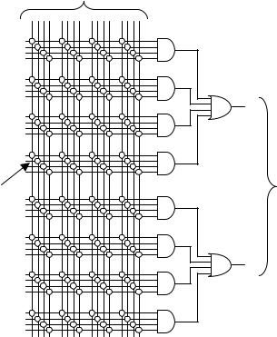
PAL (Programmable Array Logic) chips were introduced by Monolithic Memories in the mid 1970s. Its basic architecture is illustrated symbolically in figure A1, where the little circles represent programmable connections. As can be seen, the circuit is composed of a programmable array of AND gates, followed by a fixed array of OR gates.
The implementation of figure A1 was based on the fact that any combinational function can be represented by a Sum-of-Products (SOP); that is, if a1, a2, . . . , aN are the logic inputs, then any combinational output x can be computed as
x ¼ m1 þ m2 þ þ mM ;
where mi ¼ fi (a1, a2, . . . , aN ) are the minterms of the function x. For example
x ¼ a1a2 þ a2a3a4 þ a1a2a3a4a5:
TLFeBOOK
Programmable Logic Devices |
307 |
inputs
outputs
programmable interconnects
Figure A1
Illustration of PAL architecture.
Hence, the products (minterms) can be obtained by means of AND gates, whose outputs are then connected to an OR gate to compute their sum, thus implementing the SOP equation described above.
The main limitation of this approach was the fact that it allowed only the implementation of combinational functions. To circumvent this problem, registered PALs were launched toward the end of the 1970s. These included a flip-flop at each output (after the OR gates in figure A1), thus allowing the implementation of sequential functions as well (though only very simple ones).
An example of a then popular PAL chip is the PAL16L8 device, which contained 16 inputs and 8 outputs (though only 18 I/O pins were indeed available, because it was a 20-pin DIP package; there were ten IN pins, two OUT pins, and six IN/OUT
TLFeBOOK
308 |
Appendix A |
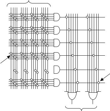
inputs
programmable programmable  interconnects interconnects
outputs
Figure A2
Illustration of PLA architecture.
pins (bidirectional), plus VCC and GND). Its registered counterpart was the 16R8 chip (where R stands for Registered).
The early technology employed in the fabrication of PAL devices was bipolar, with 5 V supply and current consumption (with open outputs) around 200 mA. The maximum frequency was of the order of 100 MHz, and the programmable cells were of PROM (fuse links) or EPROM (20min UV erase time) type.
PLA Devices
PLA (Programmable Logic Array) chips were also introduced in the mid 1970s (by Signetics). The basic architecture of a PLA is illustrated symbolically in figure A2. Comparing it with figure A1, we observe that the only fundamental di¤erence between them is that while a PAL has programmable AND connections and fixed OR
TLFeBOOK
Programmable Logic Devices |
309 |
connections, both are programmable in a PLA. The obvious advantage was greater flexibility. However, higher time constants at the internal nodes lowered the circuit speed.
An example of a then popular PLA chip is the Signetics PLS161 device. It contained 12 inputs and 8 outputs, being the AND inputs and the OR inputs all programmable. A total of 48 12-input AND gates were available, followed by a total of 8 48-input OR gates. At the outputs, additional programmable XOR gates were also available.
The technology then employed in the fabrication of PLAs was the same as that of PALs. Though PLAs are also obsolete now, they reappeared recently as a building block in the first family of low power CPLDs, the CoolRunner family (from Xilinx—to be described later).
GAL Devices
The GAL (Generic PAL) architecture was introduced by Lattice in the beginning of the 1980s. It contained several important improvements over the first PAL devices: first, a more sophisticated output cell (Macrocell) was constructed, which included, besides the flip-flop, several gates and multiplexers; second, the Macrocell itself was programmable, allowing several modes of operation; third, a ‘return’ signal from the output of the Macrocell to the programmable array was also included, conferring the circuit more versatility; fourth, EEPROM was employed instead of PROM or EPROM. An electronic signature for identification was also included.
As mentioned earlier, GAL is the only SPLD (Simple PLD) still manufactured in a standalone package. Additionally, it also serves as the basic building block in the construction of most CPLDs (there are exceptions, however, like the CoolRunner CPLD mentioned above, which employs PLAs instead).
Figure A3 shows an example of GAL device, the GAL16V8 (where V stands for Versatile). It is a 16-input, 8-output circuit in a 20-pin package. As can be seen, the actual configuration is eight IN pins (pis 2–9) and eight IN/OUT pins (pins 12–19), plus CLK (pin 1), /OE (–Output Enable, pin 11), VDD (pin 20), and GND (pin 10). At each output there is a Macrocell (after the OR gate), which contains, besides the flip-flop, logic gates and multiplexers. A feedback signal from the Macrocell to the programmable array can also be observed. The programmable interconnections are represented by small circles. Notice that this architecture directly resembles that of a PAL (figure A1), except for the presence of a macrocell at each output and the feedback signal.
Current GAL devices use CMOS technology, 3.3 V supply, EEPROM or Flash technology, and maximum frequency around 250 MHz. Several companies manufacture them (Lattice, Atmel, TI, etc.).
TLFeBOOK
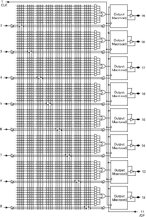
Figure A3
GAL 16V8 chip.
TLFeBOOK

Programmable Logic Devices |
311 |
||||||||||||||||
|
|
|
|
|
|
|
|
|
|
|
|
|
|
|
|
|
|
|
|
|
|
|
|
|
|
|
|
|
|
|
|
|
|
|
|
|
|
|
|
|
|
|
|
|
|
|
|
|
|
|
|
|
|
|
|
|
|
|
|
|
|
|
|
|
|
|
|
|
|
|
|
|
|
|
|
|
|
|
|
|
|
|
|
|
|
|
|
|
|
|
|
|
|
|
|
|
|
|
|
|
|
|
|
|
|
|
|
|
|
|
|
|
|
|
|
|
|
|
|
|
|
|
|
|
|
|
|
|
|
|
|
|
|
|
|
|
|
|
|
|
|
|
|
|
|
|
|
|
|
|
|
|
|
|
|
|
|
|
|
|
|
|
|
|
|
|
|
|
|
|
|
|
|
|
|
|
|
|
|
|
|
|
|
|
|
|
|
|
|
|
|
|
|
|
|
|
|
|
|
|
|
|
|
|
|
|
|
|
|
|
|
|
|
|
|
|
|
|
|
|
|
|
|
|
|
|
|
|
|
|
|
|
|
|
|
|
|
|
|
|
|
|
|
|
|
|
|
|
|
|
|
|
|
|
|
|
|
|
|
|
|
|
|
|
|
|
|
|
|
|
|
|
|
|
|
|
|
|
|
|
|
|
|
|
|
|
|
|
|
|
|
|
|
|
|
|
|
|
|
|
|
|
|
|
|
|
|
|
|
|
|
|
|
|
|
|
|
|
|
|
|
|
|
|
|
|
|
|
|
|
|
|
|
|
|
|
|
|
|
|
|
|
|
|
|
|
|
|
|
|
|
|
|
|
|
|
|
|
|
|
|
|
|
|
|
|
|
|
|
|
|
|
|
|
|
|
|
|
|
|
|
|
|
|
|
|
|
|
|
|
|
|
|
|
|
|
|
|
|
|
|
|
|
|
|
|
|
|
|
|
|
|
|
|
|
|
|
|
|
|
|
|
|
|
|
|
|
|
|
|
|
|
|
|
|
|
|
|
|
|
|
|
|
|
|
|
|
|
|
|
|
|
|
|
|
|
|
|
|
|
|
|
|
|
|
|
|
|
|
|
|
|
|
|
|
|
|
|
|
|
|
|
|
|
|
Figure A4
CPLD architecture.
A3. CPLD (Complex PLD)
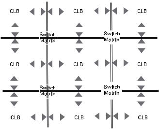
The basic approach in the construction of a CPLD is illustrated in figure A4. As shown, it consists of several PLDs (in general of GAL type) fabricated on a single chip, with a programmable switch matrix used to connect them together and to the I/O pins. Moreover, CPLDs normally contain a few additional features, like JTAG support and interface to other logic standards (1.8 V, 2.5 V, 5 V, etc.).
Regarding figure A4, as an example we can mention the Xilinx XC9500 CPLD. It consists of n PLDs, each resembling a 36V18 GAL device (therefore similar to the 16V8 architecture of figure A3, but with 36 inputs and 18 outputs, instead of 16 inputs and 8 outputs, thus with 18 Macrocells each), where n ¼ 2, 4, 6, 8, 12, or 16.
Several companies manufacture CPLDs, like Altera, Xilinx, Lattice, Atmel, Cypress, etc. Examples from two companies (Altera and Xilinx) are illustrated in tables A1 and A2. As can be seen, over 500 macrocells and over 10,000 gates can be found in these devices.
A4. FPGA
Field Programmable Gate Array (FPGA) devices were introduced by Xilinx in the mid 1980s. They di¤er from CPLDs in architecture, storage technology, number of built-in features, and cost, and are aimed at the implementation of high performance, large-size circuits.
TLFeBOOK
312 |
Appendix A |
Table A1
Altera CPLDs.
Family |
Max7000 (B, AE, S) |
MAX3000 (A) |
MAX II (G) |
||||
|
|
|
|
|
|
|
|
Macrocells/ |
32–512 macrocells |
32–512 macrocells |
240–2,210 LUTs |
||||
LUTs |
|
|
|
|
(192–1,700 equiv. macrocells) |
||
|
|
|
|
|
|
|
|
System gates |
600–10,000 |
600–10,000 |
|
|
|
||
|
|
|
|
|
|
|
|
I/O pins |
32–512 |
34–208 |
80–272 |
||||
|
|
|
|
|
|
|
|
Max. internal |
303 MHz |
227 MHz |
304 MHz |
||||
clock freq. |
|
|
|
|
(I/O limited) |
||
|
|
|
|
|
|
|
|
Supply voltage |
2.5 V (B), 3.3 V (AE), 5 V (S) |
3.3 V |
1.8 V (G), 2.5 V, 3.3 V |
||||
|
|
|
|
|
|
|
|
Interconnects |
EEPROM |
EEPROM |
Flash þ SRAM |
||||
Static current |
9 mA–450 mA |
9 mA–150 mA |
2 mA–50 mA |
||||
|
|
|
|
|
|
|
|
Technology |
0.22 u CMOS EEPROM |
0.3 u, |
0.18 u, 6-layer metal |
||||
|
4-layer metal (7000 B) |
4-layer metal |
|
|
|
||
|
|
|
|
|
|
|
|
Table A2 |
|
|
|
|
|
|
|
Xilinx CPLDs. |
|
|
|
|
|
|
|
|
|
|
|
|
|
|
|
Family |
|
XC9500 (XV, XL, ) |
|
CoolRunner XPLA3 |
|
CoolRunner II |
|
Macrocells |
|
36–288 |
|
32–512 |
|
32–512 |
|
|
|
|
|
|
|
|
|
System gates |
|
800–6,400 |
|
750–12,000 |
|
750–12,000 |
|
|
|
|
|
|
|
|
|
I/O pins |
|
34–192 |
|
36–260 |
|
33–270 |
|
|
|
|
|
|
|
|
|
Max. internal clock |
222 MHz |
|
213 MHz |
|
385 MHz |
|
|
frequency |
|
|
|
|
|
|
|
|
|
|
|
|
|
|
|
Building block |
|
GAL 54V18 (XV, XL) |
|
PLA block |
|
PLA block |
|
|
|
GAL 36V18 ( ) |
|
|
|
|
|
Supply voltage |
|
2.5 V (XV), 3.3 V |
|
3.3 V |
|
1.8 V |
|
|
|
(XL), 5 V |
|
|
|
|
|
|
|
|
|
|
|
|
|
Interconnects |
|
Flash |
|
EEPROM |
|
|
|
|
|
|
|
|
|
|
|
Technology |
|
0.35 u CMOS |
|
0.35 u CMOS |
|
0.18 u CMOS |
|
|
|
|
|
|
|
|
|
Static current |
|
11–500 mA |
|
<0.1 mA |
|
22 uA–1 mA |
|
|
|
|
|
|
|
|
|
TLFeBOOK
Programmable Logic Devices |
313 |
||||||||||||||||||||||||||||||||
|
|
|
|
|
|
|
|
|
|
|
|
|
|
|
|
|
|
|
|
|
|
|
|
|
|
|
|
|
|
|
|
|
|
|
|
|
|
|
|
|
|
|
|
|
|
|
|
|
|
|
|
|
|
|
|
|
|
|
|
|
|
|
|
|
|
|
|
|
|
|
|
|
|
|
|
|
|
|
|
|
|
|
|
|
|
|
|
|
|
|
|
|
|
|
|
|
|
|
|
|
|
|
|
|
|
|
|
|
|
|
|
|
|
|
|
|
|
|
|
|
|
|
|
|
|
|
|
|
|
|
|
|
|
|
|
|
|
|
|
|
|
|
|
|
|
|
|
|
|
|
|
|
|
|
|
|
|
|
|
|
|
|
|
|
|
|
|
|
|
|
|
|
|
|
|
|
|
|
|
|
|
|
|
|
|
|
|
|
|
|
|
|
|
|
|
|
|
|
|
|
|
|
|
|
|
|
|
|
|
|
|
|
|
|
|
|
|
|
|
|
|
|
|
|
|
|
|
|
|
|
|
|
|
|
|
|
|
|
|
|
|
|
|
|
|
|
|
|
|
|
|
|
|
|
|
|
|
|
|
|
|
|
|
|
|
|
|
|
|
|
|
|
|
|
|
|
|
|
|
|
|
|
|
|
|
|
|
|
|
|
|
|
|
|
|
|
|
|
|
|
|
|
|
|
|
|
|
|
|
|
|
|
|
|
|
|
|
|
|
|
|
|
|
|
|
|
|
|
|
|
|
|
|
|
|
|
|
|
|
|
|
|
|
|
|
|
|
|
|
|
|
|
|
|
|
|
|
|
|
|
|
|
|
|
|
|
|
|
|
|
|
|
|
|
|
|
|
|
|
|
|
|
|
|
|
|
|
|
|
|
|
|
|
|
|
|
|
|
|
|
|
|
|
|
|
|
|
|
|
|
|
|
|
|
|
|
|
|
|
|
|
|
|
|
|
|
|
|
|
|
|
|
|
|
|
|
|
|
|
|
|
|
|
|
|
|
|
|
|
|
|
|
|
|
|
|
|
|
|
|
|
|
|
|
|
|
|
|
|
|
|
|
|
|
|
|
|
|
|
|
|
|
|
|
|
|
|
|
|
|
|
|
|
|
|
|
|
|
|
|
|
|
|
|
|
|
|
|
|
|
|
|
|
|
|
|
|
|
|
|
|
|
|
|
|
|
|
|
|
|
|
|
|
|
|
|
|
|
|
|
|
|
|
|
|
|
|
|
|
|
|
|
|
|
|
|
|
|
|
|
|
|
|
|
|
|
|
|
|
|
|
|
|
|
|
|
|
|
|
|
|
|
|
|
|
|
|
|
|
|
|
|
|
|
|
|
|
|
|
|
|
|
|
|
|
|
|
|
|
|
|
|
|
|
|
|
|
|
|
|
|
|
|
|
|
|
|
|
|
|
|
|
|
|
|
|
|
|
|
|
|
|
|
|
|
|
|
|
|
|
|
|
|
|
|
|
|
|
|
|
|
|
|
|
|
|
|
|
|
|
|
|
|
|
|
|
|
|
|
|
|
|
|
|
|
|
|
|
|
|
|
|
|
|
|
|
|
|
|
|
|
|
|
|
|
|
|
|
|
|
|
|
|
Figure A5
FPGA architecture.
The basic architecture of an FPGA is illustrated in figure A5. It consists of a matrix of CLBs (Configurable Logic Blocks), interconnected by an array of switch matrices.
The internal architecture of a CLB (figure A5) is di¤erent from that of a PLD (figure A4). First, instead of implementing SOP expressions with AND gates followed by OR gates (like in SPLDs), its operation is normally based on a LUT (lookup table). Moreover, in an FPGA the number of flip-flops is much more abundant than in a CPLD, thus allowing the construction of more sophisticated sequential circuits. Besides JTAG support and interface to diverse logic levels, other additional features are also included in FPGA chips, like SRAM memory, clock multiplication (PLL or DLL), PCI interface, etc. Some chips also include dedicated blocks, like multipliers, DSPs, and microprocessors.
Another fundamental di¤erence between an FPGA and a CPLD refers to the storage of the interconnects. While CPLDs are non-volatile (that is, they make use of antifuse, EEPROM, Flash, etc.), most FPGAs use SRAM, and are therefore volatile. This approach saves space and lowers the cost of the chip because FPGAs present a very large number of programmable interconnections, but requires an external ROM. There are, however, non-volatile FPGAs (with antifuse), which might be advantageous when reprogramming is not necessary.
TLFeBOOK
314 |
Appendix A |
Figure A6
Examples of FPGA packages.
Table A3
Xilinx FPGAs.
|
Virtex II |
|
|
|
Spartan |
Spartan |
Spartan |
Family |
Pro (X) |
Virtex II |
Virtex E |
Virtex |
3 |
IIE |
II |
|
|
|
|
|
|
|
|
Logic blocks |
352– |
64– |
384– |
384– |
192– |
384– |
96– |
(CLBs) |
11,024 |
11,648 |
16,224 |
6,144 |
8,320 |
3,456 |
1,176 |
|
|
|
|
|
|
|
|
Logic cells |
3,168– |
576– |
1,728– |
1,728– |
1,728– |
1,728– |
432– |
|
125,136 |
104,882 |
73,008 |
27,648 |
74,880 |
15,552 |
5,292 |
|
|
|
|
|
|
|
|
System gates |
|
40 k– |
72 k– |
58 k– |
50 k– |
23 k– |
15 k– |
|
|
8 M |
4 M |
1.1 M |
5 M |
600 k |
200 k |
|
|
|
|
|
|
|
|
I/O pins |
204– |
88–1108 |
176–804 |
180–512 |
124–784 |
182–514 |
86–284 |
|
1,200 |
|
|
|
|
|
|
|
|
|
|
|
|
|
|
Flip-flops |
2,816– |
512– |
1,392– |
1,392– |
1,536– |
1,536– |
384– |
|
88,192 |
93,184 |
64,896 |
24,576 |
66,560 |
13,824 |
4,704 |
|
|
|
|
|
|
|
|
Max. internal |
547 |
420 |
240 |
200 |
326 |
200 |
200 |
frequency |
MHz |
MHz |
MHz |
MHz |
MHz |
MHz |
MHz |
|
|
|
|
|
|
|
|
Supply |
1.5 V |
1.5 V |
1.8 V |
2.5 V |
1.2 V |
1.8 V |
2.5 V |
voltage |
|
|
|
|
|
|
|
|
|
|
|
|
|
|
|
Interconnects |
SRAM |
SRAM |
SRAM |
SRAM |
SRAM |
SRAM |
SRAM |
|
|
|
|
|
|
|
|
Technology |
0.13 u |
0.15 u |
0.18 u |
0.22 u |
0.09 u |
|
|
|
9-layer |
8-layer |
6-layer |
5-layer |
8-layer |
|
|
|
copper |
metal |
metal |
metal |
metal |
|
|
|
CMOS |
CMOS |
CMOS |
CMOS |
CMOS |
|
|
|
|
|
|
|
|
|
|
SRAM bits |
216 k– |
72 k– |
64 k– |
32 k– |
72 k– |
32 k– |
16 k– |
(Block RAM) |
8 M |
3 M |
832 k |
128 k |
1.8 M |
288 k |
56 k |
|
|
|
|
|
|
|
|
TLFeBOOK
Programmable Logic Devices |
315 |
Table A4
Actel FPGAs.
Family |
Accelerator |
ProASIC |
MX |
SX |
eX |
|
|
|
|
|
|
Logic modules |
2,016–32,256 |
5,376–56,320 |
295–2,438 |
768–6,036 |
192–768 |
|
|
|
|
|
|
System gates |
125 k–2 M |
75 k–1 M |
3 k–54 k |
12 k–108 k |
3 k–12 k |
|
|
|
|
|
|
I/O pins |
168–684 |
204–712 |
57–202 |
130–360 |
84–132 |
|
|
|
|
|
|
Flip-flops |
1,344–21,504 |
5,376–26,880 |
147–1,822 |
512–4,024 |
128–512 |
|
|
|
|
|
|
Max. internal |
500 MHz |
250 MHz |
250 MHz |
350 MHz |
350 MHz |
frequency |
|
|
|
|
|
|
|
|
|
|
|
Supply voltage |
1.5 V |
2.5 V, 3.3 V |
3.3 V, 5 V |
2.5 V, 3.3 V, |
2.5 V, 3.3 V, |
|
|
|
|
5 V |
5 V |
|
|
|
|
|
|
Interconnects |
Antifuse |
Flash |
Antifuse |
Antifuse |
Antifuse |
|
|
|
|
|
|
Technology |
0.15 u |
0.22 u |
0.45 um |
0.22 u |
0.22 u |
|
7-layer metal |
4-layer metal |
3-layer metal |
CMOS |
CMOS |
|
CMOS |
CMOS |
CMOS |
|
|
|
|
|
|
|
|
SRAM bits |
29 k–339 k |
14 k–198 k |
2.56 k |
n.a. |
n.a. |
|
|
|
|
|
|
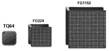
FPGAs can be very sophisticated. Chips manufactured with state-of-the-art 0.09 mm CMOS technology, with nine copper layers and over 1,000 I/O pins, are currently available. A few examples of FPGA packages are illustrated in figure A6, which shows one of the smallest FPGA packages on the left (64 pins), a medium-size package in the middle (324 pins), and a large package (1,152 pins) on the right.
Several companies manufacture FPGAs, like Xilinx, Actel, Altera, QuickLogic, Atmel, etc. Examples from two companies (Xilinx and Actel) are illustrated in tables A3 and A4. As can be seen, they can contain thousands of flip-flops and several million gates.
Notice that all Xilinx FPGAs use SRAM to store the interconnects, so are reprogrammable, but volatile (thus requiring external ROM). On the other hand, Actel FPGAs are non-volatile (they use antifuse), but are non-reprogrammable (except one family, which uses Flash memory). Since each approach has its own advantages and disadvantages, the actual application will dictate which chip architecture is most appropriate.
TLFeBOOK
TLFeBOOK
Appendix B: Xilinx ISE BModelSim Tutorial
The following synthesis, placement, and simulation tools are described in the tutorials presented in the Appendices:
Tools |
Application |
Appendix |
|
|
|
ISE 6.1 þ ModelSim 5.7c |
Xilinx CPLDs and FPGAs |
B |
MaxPlus II 10.2 þ Advanced |
Altera CPLDs and some FPGAs |
C |
Synthesis Software |
|
|
|
|
|
Quartus II 3.0 |
Altera CPLDs and FPGAs |
D |
|
|
|
XiIinx ISE 6.1 is a comprehensive synthesis and implementation environment for Xilinx programmable devices. ModelSim XE 5.7c (from Model Technology) is also provided as part of the package. The former is employed for circuit synthesis and design implementation, while the latter is used for simulation.
Xilinx ISE 6.1 WebPack, along with ModelSim XE II 5.7c Starter, can be downloaded cost-free from www.xilinx.com.
This is a very brief tutorial, which is divided into five parts:
B1. Entering VHDL Code
B2. Synthesis and Implementation
B3. Creating Testbenches
B4. Simulation (with ModelSim)
B5. Physical Realization
B1. Entering VHDL Code
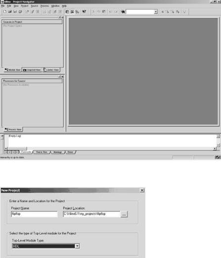
Launch ISE 6.1 Project Navigator. A screen like that of figure B1 will be displayed.
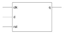
Start a new project (File ! New Project). The dialog box of figure B2 will be shown. In the Project Name field, type the name of the ENTITY of the VHDL code to be entered (flipflop, in this example). In the Project Location field, choose the working directory. Finally, select HDL as the top level module type. Click on Next.
In the dialog box of figure B3, select the device (Spartan 3, for example). Then select XST (Xilinx Synthesis Technology) as the synthesis tool, ModelSim as the simulator, and VHDL as the language. Click on Next.
TLFeBOOK
318 |
Appendix B |
Figure B1
Figure B2
TLFeBOOK
Xilinx ISE þ ModelSim Tutorial |
319 |
Figure B3
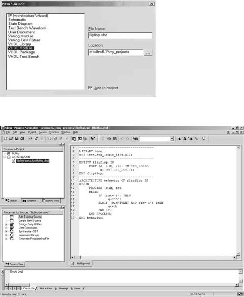
In the dialog box of figure B4, select VHDL Module, then type the file name (flipflop.vhd, in this example), and choose its location. Click on Next and Finish until the text editor is displayed, as in figure B.5.
Enter your VHDL code (figure B5) and save it. The project is now ready to be synthesized.
B2. Synthesis and Implementation
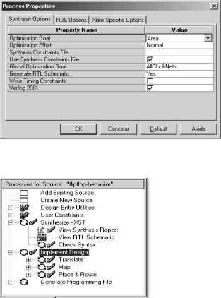
In the Processes for Source window, select Synthesize-XST. Then go to Process ! Properties. The box of figure B6 will be shown. Select Optimization Goal ¼ Area and Optimization E¤ort ¼ Normal, then click on OK.
To synthesize the design, select Process ! Run, or click on  , or double-click on Synthesize-XST. However, if desired, the syntax can be checked before synthesis is invoked. Just click on the ‘‘þ’’ sign before the word Synthesize-XST to expand it (see figure B7) and double-click on Check Syntax.
After synthesis is concluded, view the synthesis report. Double-click on View Synthesis Report, under Synthesize-XST, in the Processes for Source window (figure B7).
To better view the report, you can use the toggle tool  . A section of such a report is presented in figure B8. Check, for example, the number of flip-flops inferred by the
compiler.
Check also the RTL diagram. Double-click on View RTL Schematic, under the Synthesize-XST directory. The diagram of figure B9 will be presented.
TLFeBOOK
320 |
Appendix B |
Figure B4
Figure B5
TLFeBOOK
Xilinx ISE þ ModelSim Tutorial |
321 |
Figure B6
Figure B7
Now the design can be implemented. Double-click on the Implement Design option in the Processes for Source window (figure B7).
After the implementation is concluded, expand the Implement Design option and check the several reports produced, particularly the Pad Report (under the Place & Route directory). Check which pin was assigned to each signal.
Play with the Floorplanner. Double-click on View/Edit Placed Design (Floorplanner), under the Place & Route directory. Select View ! Hierarchy, View ! Floorplan, View ! Placement, View ! Package Pins. Now examine each one of windows created. Move the cursor over the pins of the chip to see their descriptions.
TLFeBOOK
322 |
Appendix B |
|
Release 6.1i - xst G.23 |
HDL Synthesis Report |
||||
|
=============================== |
|
|
|
|
Macro Statistics |
|
Input File Name: flipflop.prj |
# Registers: 1 |
||||
|
Output File Name : flipflop |
1-bit register: 1 |
||||
|
Output Format: NGC |
=============================== |
||||
|
Target Device: xc3s50-4-pq208 |
Cell Usage : |
||||
|
Optimization Goal: Area |
# FlipFlops/Latches: 1 |
||||
|
Optimization Effort: 1 |
# FDC: 1 |
||||
|
Keep Hierarchy: NO |
# Clock Buffers: 1 |
||||
|
Global Optimization: AllClockNets |
# BUFGP: 1 |
||||
|
RTL Output: Yes |
# IO Buffers: 3 |
||||
|
=============================== |
|
|
|
|
# IBUF: 2 |
|
Synthesizing Unit <flipflop>. |
# OBUF: 1 |
||||
|
Related source file is |
=============================== |
||||
|
c:/xilinx6.1/my_projects/flipflop.vhd. |
Device utilization summary: |
||||
|
Found 1-bit register for signal <q>. |
Selected Device : 3s50pq208-4 |
||||
|
Summary: inferred 1 D-type flip-flop(s). |
Number of Slices: 1 out of 768 0% |
||||
|
Unit <flipflop> synthesized. |
|
||||
|
|
|
|
|
|
|
|
Figure B8 |
|
||||
|
|
|
|
|
|
|
|
|
|
|
|
|
|
|
|
|
|
|
|
|
|
|
|
|
|
|
|
|
|
|
|
|
|
|
|
|
|
|
|
|
|
|
|
|
|
|
|
|
Figure B9
Note: Had a CPLD (CoolRunner, for example) been chosen instead of an FPGA (Spartan 3, in this example), the list of options in the Processes for Source window would be a little di¤erent. Try, for example, to double-click on the device description (xc3-s50. . .) in the Sources in Project window. This will bring back the dialog box of figure B3. Change the device to CoolRunner 2. Press OK and then observe the new list of options displayed in the Processes for Source window.
B3. Creating Testbenches (with HDL Bencher)
HDL Bencher allows the creation of testbenches (waveforms). Then ModelSim can be invoked to perform the actual simulation (ModelSim XE II 5.7c Starter is one of the cost-free third-party softwares provided along with Xilinx ISE 6.1 WebPack).
TLFeBOOK
Xilinx ISE þ ModelSim Tutorial |
323 |
Figure B10
Select Project ! New Source. The dialog box of figure B10 will be displayed. Select Test Bench Waveform, then type the desired file name (flipflop_tbw, for example). Finally, check whether the project location is correct and click on Next until HDL Bencher is launched (figure B11).
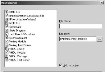
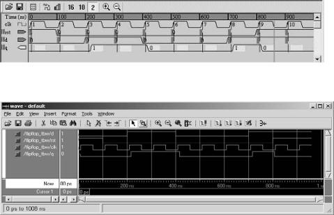
When HDL Bencher starts, a screen like that of figure B11 is displayed, which allows the clock signal to be set. Notice that the input signal clk was chosen as the master clock. Type in its parameters and then click on OK. The waveforms screen shown in figure B12 is then displayed.
The position of any signal in figure B12 can be changed by just dragging it up or
down. Also, if the clk waveform must be changed, click on  or click the right mouse button in the area under the waveforms, which will cause the dialog box of
figure B11 to be presented again.
We must now set up the values of the other signals in figure B12 (rst and d). To do so, just click on the vertical grid line after which you want the value of the signal to be changed. An example, after all input signals have been set up, is shown in figure B13.
Define the end time of the testbenches. To do so, click the right mouse button in the area under the curves and select Set End of Testbench, then drag the blue line to the desired position.
TLFeBOOK
324 |
Appendix B |
Figure B11
Figure B12
Figure B13
TLFeBOOK
Xilinx ISE þ ModelSim Tutorial |
325 |
Figure B14
Save the testbenches file. Observe that a new file (flipflop_tbw.tbw) is then added to the Sources in Project window.
B4. Simulation (with ModelSim)
Having finished creating the testbenches, ModelSim can now be invoked to perform the simulation. Indeed, several levels of simulation are available, including the following (see the complete list in the lower part of figure B14, under ModelSim Simulator):
Expected simulation results: Logical verification.
Behavioral simulation: Logical and timing verification.
Post-place & route simulation: Logical and timing verification after placement.
TLFeBOOK
326 |
Appendix B |
Figure B15
Figure B16
Two of these simulation levels will be employed in the steps below.
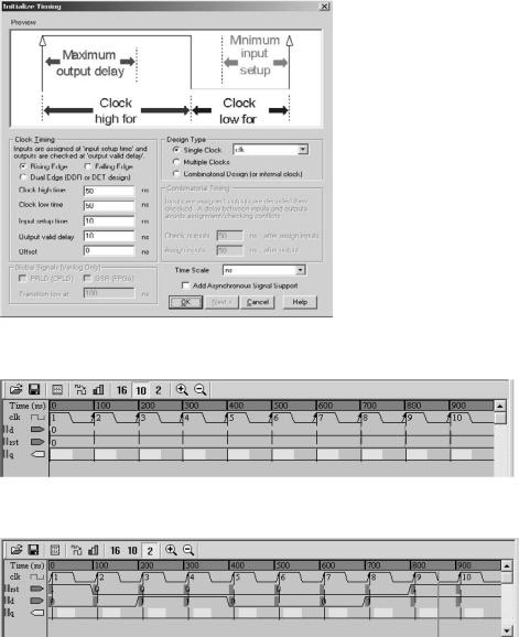
In the Sources in Project window, select the testbench file (flipflop_tbw.tbw). Notice then the several simulation options available under ModelSim Simulator in the Processes for Source window (figure B14).
Double-click on Generate Expected Simulation Results. This will run a background logical simulator, which will compute the output signals and then automatically launch HDL Bencher with the computed signals included in it. An example is shown in figure B15. Examine whether your project works as expected (from a logical point of view). Then exit HDL Bencher without saving the waveforms.
Now double-click on Simulate Post-Place & Route VHDL Model. ModelSim is launched and a detailed simulation is performed. Maximize the waveforms window and select Zoom ! Zoom Full. Examine again the results (figure B16).
TLFeBOOK
Xilinx ISE þ ModelSim Tutorial |
327 |
B5. Physical Realization
To physically implement the design in a CPLD or FPGA chip, a development kit is necessary. Inexpensive alternatives are generally available through manufacturer’s university programs, which o¤er design kits at low prices. Xilinx Digilab XC2, for example, is a development kit for Xilinx CoolRunner II devices. The development kit must be connected to a PC running ISE in order for the chip to be programmed.
Since the overall procedure of programming a chip is relatively similar from one manufacturer to another, a detailed description will be presented in only two of the appendices (C and D).
TLFeBOOK
TLFeBOOK
Appendix C: Altera MaxPlus II BAdvanced Synthesis Software Tutorial
The following synthesis, placement, and simulation tools are described in the tutorials presented in the Appendices:
Tools |
Application |
Appendix |
|
|
|
ISE 6.1 þ ModelSim 5.7c |
Xilinx CPLDs and FPGAs |
B |
MaxPlus II 10.2 þ Advanced |
Altera CPLDs and some FPGAs |
C |
Synthesis Software |
|
|
|
|
|
Quartus II 3.0 |
Altera CPLDs and FPGAs |
D |
|
|
|
MaxPlus II 10.2 Baseline from Altera is a very simple, user-friendly synthesis and simulation tool. Its main drawback is that it does not support several VHDL constructs, so only relatively simple code can be synthesized without the help of an external synthesis tool (like Leonardo Spectrum or Advanced Synthesis Software). Additionally, it only covers Altera’s basic devices (its successor, Quartus II, described in appendix D, covers all current devices). Still, due to its simplicity, it may be an adequate starting point for first-time VHDL users. Moreover, with the recent release of Advanced Synthesis Software, also a cost-free synthesis tool from Altera, using MaxPlus II became more e¤ective because Advanced Synthesis Software does support most VHDL constructs. It can be used to synthesize the VHDL code, generating an EDIF (.edf ) file which can then be imported by MaxPlus II for design implementation and simulation.
MaxPlus II 10.2 Baseline and Advanced Synthesis Software can be downloaded cost-free from www.altera.com.
This is a very brief tutorial, which is divided into five parts:
C1. Entering VHDL Code
C2. Compilation
C3. Simulation
C4. Synthesis with Advanced Synthesis Software
C5. Physical Implementation
TLFeBOOK

330 |
Appendix C |
Figure C1
C1. Entering VHDL Code
Launch MaxPlus II 10.2 Baseline.
Open the text editor (MaxPlus II ! Text Editor), or open an existing project (File !Open). A blank screen (like that of figure C1, but without the text) will be displayed.
Enter your VHDL code (a D-type flip-flop is shown in figure C1). Save it with the extension .vhd and using the same name as the ENTITY’s (flipflop.vhd, in this example).
C2. Compilation
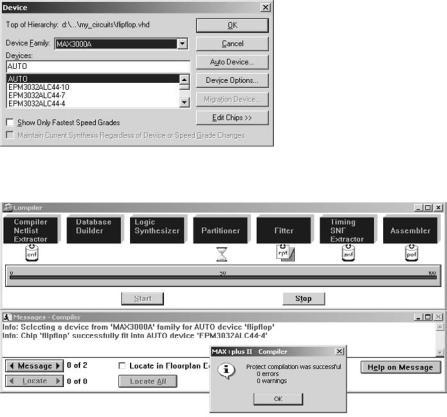
Set the project to the current file: File ! Project ! Set Project to Current File.
Choose the target device (Assign ! Device). A pull down menu will be displayed (figure C2). Select the desired device (say, Family ¼ MAX3000A, Device ¼ AUTO).
TLFeBOOK
Altera MaxPlus II þ Advanced Synthesis Software Tutorial |
331 |
Figure C2
Figure C3
Set up the optimizer. The implementation can be optimized for speed or for area. Select Assign ! Global Project Logic Synthesis and move the Optimize cursor all the way to the left (value ¼ 0) to optimize for area, or all the way to the right (value ¼ 10) to optimize for speed. Values in between can also be used.
Click on the Compiler icon  , then on Start, in order to execute the compilation.
If no errors are detected, a screen like that of figure C3 is shown. It displays the files created during the compilation in the upper part (notice, for example, the report ‘‘rpt’’ file icon), and information regarding the chip and fitter in the lower part.
Open the report (.rpt) file (double-click on its icon, shown in figure C3). Verify at least the following: pin assignments and number of logic cells and flip-flops used to
TLFeBOOK

332 |
Appendix C |
|
|
R |
|
|
|
|
|
|
|
|
|
R |
|
|
|
|
E |
|
|
|
|
|
|
|
|
|
E |
|
|
|
|
S |
|
|
V |
|
|
|
|
|
|
S |
|
|
|
|
E |
|
|
C |
|
|
|
|
|
|
E |
|
|
|
|
R |
|
|
C |
|
|
|
|
|
|
R |
|
|
|
|
V |
r |
|
I |
G |
G |
G |
c |
G |
|
V |
|
|
|
|
E |
s |
|
N |
N |
N |
N |
l |
N |
|
E |
|
|
|
|
D t d T D D D k D q D |
|
|
||||||||||
|
|
-----------------------------------_ |
||||||||||||
|
/ |
6 |
5 |
4 |
3 |
2 |
1 |
44 |
43 |
42 |
41 |
40 |
|
| |
#TDI |
| |
7 |
|
|
|
|
|
|
|
|
|
|
39 |
| RESERVED |
RESERVED |
| |
8 |
|
|
|
|
|
|
|
|
|
|
38 |
| #TDO |
RESERVED |
| |
9 |
|
|
|
|
|
|
|
|
|
|
37 |
| RESERVED |
GND |
| 10 |
|
|
|
|
|
|
|
|
|
36 |
| GND |
||
RESERVED |
| 11 |
|
|
|
|
|
|
|
|
|
|
35 |
| VCCIO |
|
RESERVED |
| 12 |
|
|
EPM3032ALC44-4 |
|
|
|
34 |
| RESERVED |
|||||
#TMS |
| 13 |
|
|
|
|
|
|
|
|
|
|
33 |
| RESERVED |
|
RESERVED |
| 14 |
|
|
|
|
|
|
|
|
|
|
32 |
| #TCK |
|
VCCIO |
| 15 |
|
|
|
|
|
|
|
|
|
|
31 |
| RESERVED |
|
RESERVED |
| 16 |
|
|
|
|
|
|
|
|
|
|
30 |
| GND |
|
GND |
| 17 |
|
|
|
|
|
|
|
|
|
|
29 |
| RESERVED |
|
|
|_ |
18 19 20 |
21 22 23 24 25 26 27 28 |
|
_| |
|||||||||
|
------------------------------------ |
|
||||||||||||
|
|
R R R R G V R R R R R |
|
|
||||||||||
|
|
E E E E N C E E E E E |
|
|
||||||||||
|
|
S S S S D C S S S S S |
|
|
||||||||||
|
|
E |
E |
E |
E |
|
I |
E |
E |
E |
E |
E |
|
|
|
|
R |
R |
R |
R |
|
N |
R |
R |
R |
R |
R |
|
|
|
|
V |
V |
V |
V |
|
T |
V |
V |
V |
V |
V |
|
|
|
|
E |
E |
E |
E |
|
|
E |
E |
E |
E |
E |
|
|
|
|
D |
D |
D |
D |
|
|
D |
D |
D |
D |
D |
|
|
Total bidirectional pins required: |
0 |
|
Total reserved pins required |
4 |
|
Total logic cells required: |
1 |
|
Total flipflops required: |
|
1 |
Total product terms required: |
2 |
|
Total logic cells lending |
parallel expanders: |
0 |
Total shareable expanders |
in database: |
0 |
Synthesized logic cells: 0/32 (0%)
Figure C4
TLFeBOOK

Altera MaxPlus II þ Advanced Synthesis Software Tutorial |
333 |
Figure C5
Figure C6
construct the circuit. A little section of the report file from the design of figure C1 is shown in figure C4.
C3. Simulation
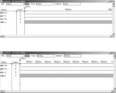
Open the waveform editor (MaxPlus II ! Waveform Editor). A blank screen like that of figure C5 will be displayed (without the box in the center).
With the cursor inside the window of figure C5, press the right mouse button. A pull down menu like that in the center of figure C5 will be shown. Select Enter Nodes from SNF. The dialog box of figure C6 will then be presented. Click on List, then
TLFeBOOK
334 |
Appendix C |
Figure C7
Figure C8
on ¼>, and finally on OK. All signals listed in the ENTITY of the VHDL code will appear in the waveform window (see figure C7). Notice that the default value for the input signals is 0, while for the outputs it is X (unknown).
Before establishing the values of the signals, define the length of the waveforms and the grid size. To set the length, select File ! End Time and type 1us. To set the grid, select Options ! Grid Size and type 50 ns. Finally, select View ! Fit in Window. You can also change the order of the signals by just dragging them up or down. For example, to have clk as the first signal, just place the cursor on the arrow that precedes the word clk, then press and hold the left mouse button and drag clk to the desired position. The window will then look like that of figure C8.
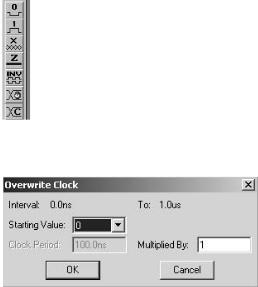
We must now define the input signals, so the tools of figure C9 can be used. The clock icon  is used for pulse generators,
  to set the logic value 0,
  for logic
TLFeBOOK
Altera MaxPlus II þ Advanced Synthesis Software Tutorial |
335 |
Figure C9
Figure C10
value 1,  for counters (incremental bus values), and
  for a group value (bus with a fixed value).
Start with clk. Select the corresponding line (click the left mouse button on the
word clk), then click on  (figure C9), which will cause the dialog box of figure C10 to be displayed. Type Starting Value 0 and Multiplied By 1, then click on OK
(Multiplied by 1 means that the period corresponds to one pair of time slots, with each time slot corresponding to one grid space; in this case, period ¼ 100 ns).
Set up the other input signals. For rst, select the first two time slots (0 to 100 ns).
Then click on  to change its value to 1 in this interval. Next, select the entire line of d (click the left mouse button on the word d) and click on
  again. Type Multiplied By 4 and click on OK. The waveforms should then look like those in figure
C11.
Save your waveforms with the extension .scf (flipflop.scf ).
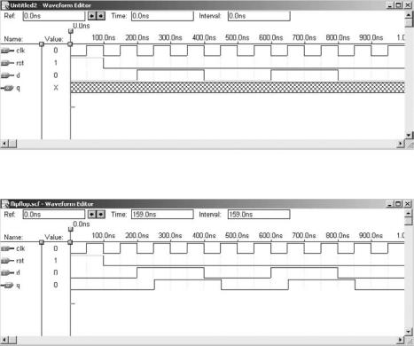
Now the design is ready to be simulated. Click on the simulator icon  and on Start. The simulator will automatically fill in all output signals in the waveform edi-
tor (q, in this example). The result is shown in figure C12.
TLFeBOOK
336 |
Appendix C |
Figure C11
Figure C12
C4. Synthesis with Advanced Synthesis Software
To overcome the limitations of MaxPlus II, which does not support several VHDL constructs, Advanced Synthesis Software was recently released. It can be used to synthesize the VHDL code, giving origin to an EDIF (.edf ) file, which can then be imported by MaxPlus II to finish the design (fitting, simulation, programming). As mentioned earlier, Advanced Synthesis Software can also be downloaded cost-free from www.altera.com.
Using a text editor, type your VHDL code. Suggestion: Since MaxPlus II will be used for fitting and simulation anyway, launch it and type the VHDL code using
TLFeBOOK
Altera MaxPlus II þ Advanced Synthesis Software Tutorial |
337 |
Figure C13
MaxPlus II’s own text editor, as described in section C1 above. Save the file with the extension .vhd and the same name as the ENTITY’s (flipflop.vhd).
Launch Advanced Synthesis Software. A screen like that of figure C13 will be displayed.
Open a new project (File ! New Project). In the dialog box, type the name of the project (same as the ENTITY’s). The project will be saved with the extension
.max2syn (flipflop.max2syn)
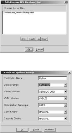
Assign the VHDL file to the project (Assign ! Add/remove HDL files). The box of figure C14 will be displayed. Click on Add, select the file, then click on Open and OK.
Click on the synthesis settings icon  . The dialog box of figure C15 will be presented. Choose the target device (MAX3000A, for example) and VHDL93.
Click on the synthesis icon  . If no syntax errors are detected, an EDIF file will be generated, with the extension .edf and the same name as the project’s (flipflop.edf ).
Return to MaxPlus II and import the EDIF file just created by Advanced Synthesis Software (File ! Open). Then start from the beginning of section C2 above, in order to compile the new design.
TLFeBOOK
338 |
Appendix C |
Figure C14
Figure C15
C5. Physical Implementation
In this section, we will describe the process of physically implementing a circuit on a CPLD. In this description, Altera’s UP1 development kit will be utilized, which is furnished as part of their University Program. Other options are also available, either from Altera or other companies. Indeed, most CPLD/FPGA manufacturers o¤er low-cost development kits as part of their university programs.
The Altera UP1 Board
A view of the Altera UP1 kit is shown in figure C16. As can be seen, it contains two devices:
TLFeBOOK
Altera MaxPlus II þ Advanced Synthesis Software Tutorial |
339 |
Figure C16
EPM7128SLC84-7 (from the MAX7000S family): This is a CPLD (appendix A) in an 84-pin package. It contains 128 macrocells, each having a PAL-type architecture and one flip-flop.
EPF10K20RC240-4 (from the FLEK10K family): This is an FPGA (appendix A) in a 240-pin package. It consists of 1,152 LEs (logic elements), each with a 4-bit LUT (lookup table) and one flip-flop.
For testing the CPLD, the board contains eight LEDs (light emitting diodes), two SSDs (seven-segment displays), and two eight-bit dip switches (figure C16). And, for testing the FPGA, 2 more SSDs and another eight-bit dip switch. The LEDs and the segments of the SSDs use negative logic, thus being turned on when 0 V is applied. The switches, on the other hand, provide 5 V signals when moved up or 0 V when moved down.
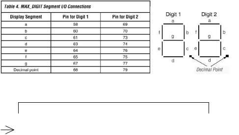
The LEDs and switches are not connected to any of the chip pins, so they can be freely wired to the devices to satisfy any particular setup. However, the segments of the SSDs are already connected, thus requiring the implemented circuit to have specific pin assignments. In the case of the CPLD, the pins to which the SSDs are connected are those listed in figure C17.
The board also contains a 25.175 MHz clock, which is connected to the devices (the global clock pin of the CPLD is pin 83).
TLFeBOOK
340 |
Appendix C |
Figure C17
Table 2. JTAG Jumper Settings
Desired Action |
TDI |
TDO |
DEVICE |
BOARD |
|
|
|
|
|
Program EPM7128S device |
C1 & C2 |
C1 & C2 |
C1 & C2 |
C1 & C2 |
only |
|
|
|
|
Configure FLEX 10k device |
C2 & C3 |
C2 & C3 |
C1 & C2 |
C1 & C2 |
only |
|
|
|
|
Program/configure both |
C2 & C3 |
C1 & C2 |
C2 & C3 |
C1 & C2 |
devices |
|
|
|
|
Connect multiple boards |
C2 & C3 |
OPEN |
C2 & C3 |
C2 & C3 |
together |
|
|
|
|
Figure C18
The complete specifications of the board are available at www.altera.com/ literature/univ/upds.pdf.
Setting up the UP1 Board
In the description presented below, the CPLD (EPM7128SLC84-7) will be used as the target device. Therefore, the jumpers in the TDO, TDI, DEVICE, and BOARD columns (see figure C16, right above the EPM7128S device) should all be installed in the upper position (that is, between the upper two pins, C1 and C2, of each column of pins, as indicated in the table of figure C18).
Connect the ByteBlaster cable provided with the kit between the board and the parallel port of the PC.
Connect the DC supply (9 V) to the board. Notice that the Power LED and two SSDs are lit.
TLFeBOOK
Altera MaxPlus II þ Advanced Synthesis Software Tutorial |
341 |
Figure C19
Implementing the Design
We will assume that MaxPlus II 10.2 Baseline is open and that the VHDL code has already been entered and debugged, following the steps described in the previous sections of this appendix.
Assign the target device by selecting Assign ! Device and choosing Family ¼ MAX7000S and Device ¼ EPM7128SLC84-7 (do not check the Select Only Fastest Speed Grade box).
Compile the circuit as before (click on  ).
).
Open the report (rpt) file and check which pin was assigned to each signal. If no changes are required, proceed to the next section. To change pins, proceed in the paragraph below.
To choose a pin for clock di¤erent from the automatic global clock assignment (pin 83), first go to Assign ! Global Project Logic Synthesis and unmark the box Clock under Automatic Global.
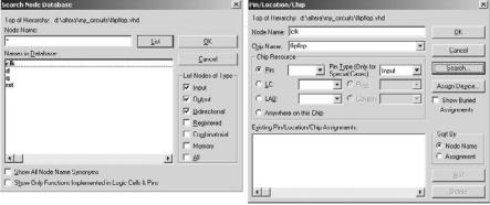
To choose the pins, select Assign ! Pin/Location/Chip ! Search ! List. A dialog box like that on the left of figure C19 will be displayed. Select a signal and click on OK, thus displaying the box on the right of figure C19. Choose the pin number and the pin type (input, output, etc.), then click on OK if that is the only pin to be changed, or on Add to continue the procedure.
Upon returning to the main window of MaxPlus II, recompile your design. Then open the report (rpt) file (by clicking on the ‘rpt’ icon) and confirm that the pins were indeed assigned as expected.
TLFeBOOK
342 |
Appendix C |
Figure C20
Downloading the Design
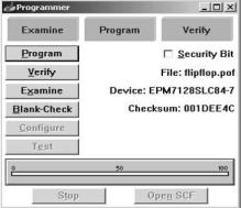
Your design is now ready to be downloaded onto the chip.
Double-click on the pof (program object file) icon (shown at the end of compilation, figure C3). A box like that of figure C20 will be displayed.
Select, in the main menu, Options ! Hardware Setup ! ByteBlaster(MV), then click on OK.
Finally, in the screen of figure C20, click on Program to program the device. After a few moments, the chip will be ready to be physically tested and/or used.
TLFeBOOK
Appendix D: Altera Quartus II Tutorial
The following synthesis, placement, and simulation tools are described in the tutorials presented in the Appendices:
Tools |
Application |
Appendix |
|
|
|
ISE 6.1 þ ModelSim 5.7c |
Xilinx CPLDs and FPGAs |
B |
MaxPlus II 10.2 þ Advanced |
Altera CPLDs and some FPGAs |
C |
Synthesis Software |
|
|
|
|
|
Quartus II 3.0 |
Altera CPLDs and FPGAs |
D |
|
|
|
Quartus II 3.0 from Altera is a comprehensive integrated compiler, placement, and simulation tool. It allows the complete design, from VHDL code to physical implementation, of projects using any of Altera’s FPGA or CPLD devices. Quartus II is the successor of MaxPlus II (Appendix C).
Quartus II 3.0 Web Edition can be downloaded cost-free from www.altera.com. This is a very brief tutorial, which is divided into four parts:
D1. Entering VHDL Code
D2. Compilation
D3. Simulation
D4. Physical Implementation
D1. Entering VHDL Code
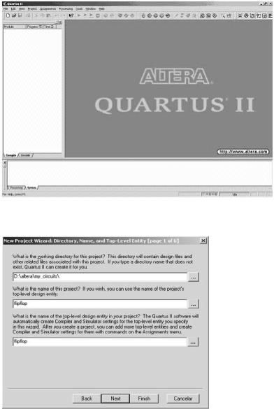
Launch Quartus II 3.0. A window like that of figure D1 will be displayed.
Create a new project (File ! New Project Wizard). The dialog box of figure D2 will appear. Select the working directory in the first field, and the project name (same as the ENTITY’s) in the second. The last field will be automatically filled with the project name (you may change it if you want). In the example below, the working directory is d:\altera\my_circuits, and the project name is flipflop. A new project, called flipflop.quartus, is then created in the working directory, which will contain the flipflop.vhd file to be created.
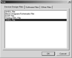
Open the text editor (File ! New, or click on  ). The menu of figure D3 will then be displayed. Select VHDL File. A blank screen will be presented.
TLFeBOOK
344 |
Appendix D |
Figure D1
Figure D2
TLFeBOOK
Altera Quartus II Tutorial |
345 |
Figure D3
Enter your VHDL code (as in figure D4). Save it with the extension .vhd (the same name as the ENTITY’s will be automatically assigned to the file, that is, flipflop.vhd in this example).
Check for syntax errors. Select Processing ! Analyze Current File, or simply click
on the analysis icon  . Any error detected by the compiler will be described in the bottom window.
D2. Compilation
Select the target device (Assignments ! Devices). A menu like that of figure D5 will be displayed. Choose the desired device Family (MAX3000A, for example). In the Target device option, you may select Auto device. In the Package, Pin count, and Speed grade options, select Any.
To compile your VHDL code, select Processing ! Start Compilation, or click on
 . If successful, a window like that of figure D6 will be displayed.
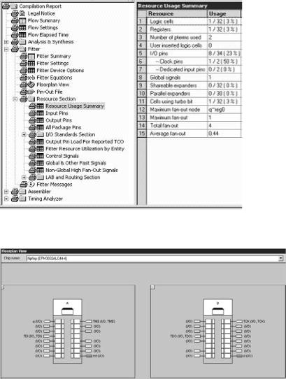
Examine the compilation reports (listed on the left of figure D6). Check at least the following:
(a) Flow Summary: This report is displayed automatically at the end of compilation, as shown in figure D6. It contains the part number of the device, the number of pins used, and the usage of the device (number of logic cells used / total number of logic cells).
TLFeBOOK
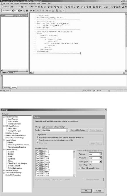
346 |
Appendix D |
Figure D4
Figure D5
TLFeBOOK

Altera Quartus II Tutorial |
347 |
Figure D6
(b)Resource Usage Summary (Fitter ! Resource Section ! Resource Usage Summary): This report (figure D7) shows details regarding the number of registers inferred from the code, logic cells used, I/O pins, etc.
(c)Input and Output Pins (Fitter ! Resource Section ! Input Pins, Fitter ! Resource Section ! Output Pins): These two reports show the I/O pin assignments.
(d)Floorplan View (Fitter ! Floorplan View): Shows a layout of the logic cells, which logic cells were used and how, etc. (see figure D8).
(e)Analysis and Synthesis Equations (Analysis and Synthesis ! Analysis and Synthesis Equations): Contains the logical equations implemented by the compiler (logical operations þ registers).
D3. Simulation
Open the Waveform Editor. To do so, select File ! New ! Other File ! Vector
Waveform File, or simply click on  . A screen like that of figure D9 will be displayed.
In order to define the size of the waveforms (figure D9), do:
Edit ! End Time (select 500 ns, for example).
Edit ! Grid Size (select Period ¼ 50 ns, Duty Cycle ¼ 50%). Finally, select View ! Fit in Window.
Note: To change the default values, go to Tools ! Options ! Waveform Editor ! General.
TLFeBOOK
348 |
Appendix D |
Figure D7
Figure D8
TLFeBOOK
Altera Quartus II Tutorial |
349 |
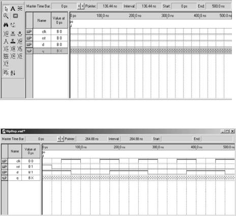
Figure D9
Figure D10
Add the input and output signals to the waveform window. To do so, click the right mouse button inside the white area under Name (figure D9) and select Insert Node or Bus. In the next box, select Node Finder. A screen like that of figure D10 will then be shown. Make sure that Filter is set to Pins: all. Click on Start, then on X, and finally on OK. The waveforms window will now contain a list of all signals described in the ENTITY of the VHDL code, as shown in figure D11. Notice that the input signals (clk, rst, d) are indicated by an inward arrow with an ‘‘I’’ inside, while the output signal (q) is represented by an outward arrow with an ‘‘O’’ inside. The position of the signals can be rearranged by simply dragging them up or down (for example, one might want rst to come right below clk).
TLFeBOOK
350 |
Appendix D |
Figure D11
Figure D12
We have to set now the values of the input signals (clk, rst, and d in figure D11). The easiest way is by using the waveform menu (shown on the left-hand side of figure D11). To set up the clock signal, select the entire clk line (by clicking on the arrow
with an I inside beside the word clk) and then click on  . A setup box will be displayed. Choose Period ¼ 100 ns.
For rst, select only its first portion (from 0 to 25 ns), then click on  , which will cause the selected portion to change its logic level from 0 to 1.
Finally, we have to set up the value of d. Select the entire d line, then click on  . Choose Period ¼ 200 ns and Phase ¼ 75 ns. The result is shown in figure D12.
TLFeBOOK
Altera Quartus II Tutorial |
351 |
Figure D13
Notice that q is not available yet, for it will be determined by the simulator. Save the waveform as flipflop.vwf.
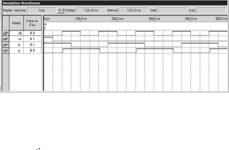
The system is now ready for simulation. Select Processing ! Start Simulation, or just click on  . The result should look like that in figure D13.
D4. Physical Implementation
Development kit: To perform the physical implementation, we will assume that an Altera UP1 (or UP2) kit is available (this development kit was described in section C5 of appendix C). The kit must be connected to the parallel port of the PC by means of a ByteBlaster cable (provided with the kit).
Device selection: The kit (Altera UP1 or UP2) contains two devices, EPM7128SLC84-7 (a CPLD from the MAX7000S family) and EPF10K70RC240-4 (an FPGA from the FLEX10K family). Therefore, in the Assignments ! Devices step of section D2, one of these two devices must be selected.
Changing pin assignments: The I/O pins are automatically assigned during compilation. However, if desired, the assignments can be changed. Select Assignments ! Assign Pins, which will cause the window of figure D14 to be opened. Say that we
want rst to be connected to pin 4, for example. Select pin 4, then click on  , which will open the window of figure D10. Click on Start, select rst on the left column, then click on > and OK. Upon returning to the window of figure D14, click on Add. Repeat this process for any other changes of pin assignments.
TLFeBOOK
352 |
Appendix D |
Figure D14
Figure D15
TLFeBOOK
Altera Quartus II Tutorial |
353 |
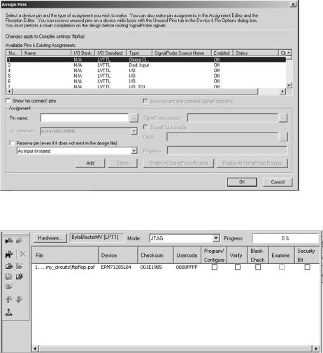
Setting up the Programmer: To download the program to the kit (device), first
select Tools ! Programmer, or click on  . The window of figure D15 will be shown. In the Hardware option, ByteBlasterMV (LPT1) should appear. If not, click
on Hardware, then on Select Hardware, select ByteBlasterMV, and finally click on Add Hardware. Returning to the window of figure D15, in the File column verify that the design file, with the extension .pof (program object file), is present. Then check the box under Program/Configure.
Programming the device: Finally, the device can be programmed. Just select Processing ! Start Programming. After a few moments, programming will be concluded and the chip ready to be physically tested and/or used.
TLFeBOOK
TLFeBOOK