


6Sequential Code
As mentioned in chapter 5, VHDL code is inherently concurrent. PROCESSES, FUNCTIONS, and PROCEDURES are the only sections of code that are executed sequentially. However, as a whole, any of these blocks is still concurrent with any other statements placed outside it.
One important aspect of sequential code is that it is not limited to sequential logic. Indeed, with it we can build sequential circuits as well as combinational circuits. Sequential code is also called behavioral code.
The statements discussed in this section are all sequential, that is, allowed only inside PROCESSES, FUNCTIONS, or PROCEDURES. They are: IF, WAIT, CASE, and LOOP.
VARIABLES are also restricted to be used in sequential code only (that is, inside a PROCESS, FUNCTION, or PROCEDURE). Thus, contrary to a SIGNAL, a VARIABLE can never be global, so its value can not be passed out directly.
We will concentrate on PROCESSES here. FUNCTIONS and PROCEDURES are very similar, but are intended for system-level design, being therefore seen in Part II of this book.
6.1PROCESS
A PROCESS is a sequential section of VHDL code. It is characterized by the presence of IF, WAIT, CASE, or LOOP, and by a sensitivity list (except when WAIT is used). A PROCESS must be installed in the main code, and is executed every time a signal in the sensitivity list changes (or the condition related to WAIT is fulfilled). Its syntax is shown below.
[label:] PROCESS (sensitivity list)
[VARIABLE name type [range] [:= initial_value;]] BEGIN
(sequential code) END PROCESS [label];
VARIABLES are optional. If used, they must be declared in the declarative part of the PROCESS (before the word BEGIN, as indicated in the syntax above). The initial value is not synthesizable, being only taken into consideration in simulations.
The use of a label is also optional. Its purpose is to improve code readability. The label can be any word, except VHDL reserved words (appendix E).
TLFeBOOK

92 |
Chapter 6 |
d |
|
|
|
q |
|
|
DFF
clk
rst
Figure 6.1
DFF with asynchronous reset of example 6.1.
Figure 6.2
Simulation results of example 6.1.
To construct a synchronous circuit, monitoring a signal (clock, for example) is necessary. A common way of detecting a signal change is by means of the EVENT attribute (seen in section 4.2). For instance, if clk is a signal to be monitored, then clk’EVENT returns TRUE when a change on clk occurs (rising or falling edge). An example, illustrating the use of EVENT and PROCESS, is shown next.
Example 6.1: DFF with Asynchronous Reset #1
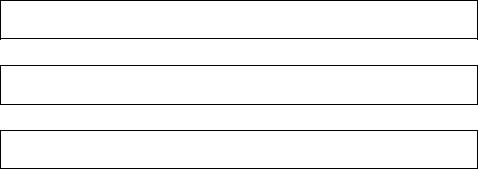
A D-type flip-flop (DFF, figure 6.1) is the most basic building block in sequential logic circuits. In it, the output must copy the input at either the positive or negative transition of the clock signal (rising or falling edge).
In the code presented below, we make use of the IF statement (discussed in section 6.3) to design a DFF with asynchronous reset. If rst ¼ ‘1’, then the output must be q ¼ ‘0’ (lines 14–15), regardless of the status of clk. Otherwise, the output must copy the input (that is, q ¼ d) at the positive edge of clk (lines 16–17). The EVENT attribute is used in line 16 to detect a clock transition. The PROCESS (lines 12–19) is run every time any of the signals that appear in its sensitivity list (clk and rst, line 12) changes. Simulation results, confirming the functionality of the synthesized circuit, are presented in figure 6.2.
TLFeBOOK
Sequential Code |
93 |
1 --------------------------------------
2LIBRARY ieee;
3 USE ieee.std_logic_1164.all;
4 --------------------------------------
5ENTITY dff IS
6PORT (d, clk, rst: IN STD_LOGIC;
7 |
q: OUT STD_LOGIC); |
8 |
END dff; |
9 |
-------------------------------------- |
10 |
ARCHITECTURE behavior OF dff IS |
11BEGIN
12PROCESS (clk, rst)
13BEGIN
14IF (rst='1') THEN
15q <= '0';
16ELSIF (clk'EVENT AND clk='1') THEN
17q <= d;
18END IF;
19END PROCESS;
20END behavior;
21 --------------------------------------
6.2Signals and Variables
Signals and variables will be studied in detail in the next chapter. However, it is impossible to discuss sequential code without knowing at least their most basic characteristics.
VHDL has two ways of passing non-static values around: by means of a SIGNAL or by means of a VARIABLE. A SIGNAL can be declared in a PACKAGE, ENTITY or ARCHITECTURE (in its declarative part), while a VARIABLE can only be declared inside a piece of sequential code (in a PROCESS, for example). Therefore, while the value of the former can be global, the latter is always local.
The value of a VARIABLE can never be passed out of the PROCESS directly; if necessary, then it must be assigned to a SIGNAL. On the other hand, the update of a VARIABLE is immediate, that is, we can promptly count on its new value in the next line of code. That is not the case with a SIGNAL (when used in a PROCESS), for its new value is generally only guaranteed to be available after the conclusion of the present run of the PROCESS.
TLFeBOOK

94 |
Chapter 6 |
Finally, recall from section 4.1 that the assignment operator for a SIGNAL is ‘‘<¼’’ (ex.: sig <¼ 5), while for a VARIABLE it is ‘‘:¼’’ (ex.: var :¼ 5).
6.3 IF
As mentioned earlier, IF, WAIT, CASE, and LOOP are the statements intended for sequential code. Therefore, they can only be used inside a PROCESS, FUNCTION, or PROCEDURE.
The natural tendency is for people to use IF more than any other statement. Though this could, in principle, have a negative consequence (because the IF/ELSE statement might infer the construction of an unnecessary priority decoder), the synthesizer will optimize the structure and avoid the extra hardware. The syntax of IF is shown below.
IF conditions THEN assignments; ELSIF conditions THEN assignments;
...
ELSE assignments; END IF;
Example:
IF (x<y) THEN temp:="11111111";
ELSIF (x=y AND w='0') THEN temp:="11110000";
ELSE temp:=(OTHERS =>'0');
Example 6.2: One-digit Counter #1
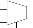
The code below implements a progressive 1-digit decimal counter (0 ! 9 ! 0). A top-level diagram of the circuit is shown in figure 6.3. It contains a single-bit input
C
O
U
clk N  digit (3:0)
T
E
R
Figure 6.3
Counter of example 6.2.
TLFeBOOK

Sequential Code |
95 |
Figure 6.4
Simulation results of example 6.2.
(clk) and a 4-bit output (digit). The IF statement is used in this example. A variable, temp, was employed to create the four flip-flops necessary to store the 4-bit output signal. Simulation results, confirming the correct operation of the synthesized circuit, are shown in figure 6.4.
1 ---------------------------------------------
2LIBRARY ieee;
3 USE ieee.std_logic_1164.all;
4 ---------------------------------------------
5ENTITY counter IS
6PORT (clk : IN STD_LOGIC;
7 |
digit : OUT INTEGER RANGE 0 TO 9); |
|
8 |
END counter; |
|
9 |
--------------------------------------------- |
|
10 ARCHITECTURE |
counter OF counter IS |
|
11BEGIN
12count: PROCESS(clk)
13VARIABLE temp : INTEGER RANGE 0 TO 10;
14BEGIN
15IF (clk'EVENT AND clk='1') THEN
16temp := temp + 1;
17IF (temp=10) THEN temp := 0;
18END IF;
19END IF;
20digit <= temp;
21END PROCESS count;
22END counter;
23 ---------------------------------------------
Comment: Note that the code above has neither a reset input nor any internal initialization scheme for temp (and digit, consequently). Therefore, the initial value of
TLFeBOOK

96 |
Chapter 6 |
temp in the physical circuit can be any 4-bit value. If such value is below 10 (see line 17), the circuit will count correctly from there. On the other hand, if the value is above 10, a number of clock cycles will be used until temp reaches full count (that is, 15, or ‘‘1111’’), being thus automatically reset to zero, from where the correct operation then starts. The possibility of wasting a few clock cycles in the beginning is generally not a problem. Still, if one does want to avoid that, temp ¼ 10, in line 17, can be changed to temp ¼> 10, but this will increase the hardware. However, if starting exactly from 0 is always necessary, then a reset input should be included (as in example 6.7).
Notice in the code above that we increment temp and compare it to 10, with the purpose of resetting temp once 10 is reached. This is a typical approach used in counters. Notice that 10 is a constant, so a comparator to a constant is inferred by the compiler, which is a relatively simple circuit to construct. However, if instead of a constant we were using a programmable parameter, then a full comparator would need to be implemented, which requires substantially more logic than a comparator to a constant. In this case, a better solution would be to load temp with such a parameter, and then decrement it, reloading temp when the 0 value is reached. In this case, our comparator would compare temp to 0 (a constant), thus avoiding the generation of a full comparator.
Example 6.3: Shift Register
Figure 6.5 shows a 4-bit shift register. The output bit (q) must be four positive clock edges behind the input bit (d). It also contains an asynchronous reset, which must force all flip-flop outputs to ‘0’ when asserted. In this example, the IF statement is again employed.
1 --------------------------------------------------
2LIBRARY ieee;
3USE ieee.std_logic_1164.all;
4--------------------------------------------------
d |
|
|
DFF |
|
|
DFF |
|
|
DFF |
|
|
DFF |
|
q |
|
|
|
|
|
|
|
|
|
||||||
|
|
|
|
|
|
|
|
|
|
|||||
|
|
|
|
|
|
|
|
|
|
|
|
|
|
|
|
|
|
|
|
|
|
|
|
|
|
|
|
|
|
clk rst
Figure 6.5
Shift register of example 6.3.
TLFeBOOK

Sequential Code |
97 |
5ENTITY shiftreg IS
6 |
GENERIC (n: INTEGER := 4); |
-- # of stages |
7PORT (d, clk, rst: IN STD_LOGIC;
8 |
q: OUT STD_LOGIC); |
9 |
END shiftreg; |
10 |
-------------------------------------------------- |
11 |
ARCHITECTURE behavior OF shiftreg IS |
12SIGNAL internal: STD_LOGIC_VECTOR (n-1 DOWNTO 0);
13BEGIN
14PROCESS (clk, rst)
15BEGIN
16IF (rst='1') THEN
17internal <= (OTHERS => '0');
18ELSIF (clk'EVENT AND clk='1') THEN
19internal <= d & internal(internal'LEFT DOWNTO 1);
20END IF;
21END PROCESS;
22q <= internal(0);
23END behavior;
24 --------------------------------------------------
Simulation results are shown in figure 6.6. As can be seen, q is indeed four positive clock edges behind d.
6.4WAIT
The operation of WAIT is sometimes similar to that of IF. However, more than one form of WAIT is available. Moreover, contrary to when IF, CASE, or LOOP are
Figure 6.6
Simulation results of example 6.3.
TLFeBOOK
98 |
Chapter 6 |
used, the PROCESS cannot have a sensitivity list when WAIT is employed. Its syntax (there are three forms of WAIT) is shown below.
WAIT UNTIL signal_condition;
WAIT ON signal1 [, signal2, ... ];
WAIT FOR time;
The WAIT UNTIL statement accepts only one signal, thus being more appropriate for synchronous code than asynchronous. Since the PROCESS has no sensitivity list in this case, WAIT UNTIL must be the first statement in the PROCESS. The PROCESS will be executed every time the condition is met.
Example: 8-bit register with synchronous reset.
PROCESS |
-- no sensitivity list |
BEGIN |
|
WAIT UNTIL (clk'EVENT AND clk='1');
IF (rst='1') THEN
output <= "00000000";
ELSIF (clk'EVENT AND clk='1') THEN output <= input;
END IF;
END PROCESS;
WAIT ON, on the other hand, accepts multiple signals. The PROCESS is put on hold until any of the signals listed changes. In the example below, the PROCESS will continue execution whenever a change in rst or clk occurs.
Example: 8-bit register with asynchronous reset.
PROCESS
BEGIN
WAIT ON clk, rst;
IF (rst='1') THEN
TLFeBOOK
Sequential Code |
99 |
output <= "00000000";
ELSIF (clk'EVENT AND clk='1') THEN output <= input;
END IF;
END PROCESS;
Finally, WAIT FOR is intended for simulation only (waveform generation for testbenches). Example: WAIT FOR 5ns;
Example 6.4: DFF with Asynchronous Reset #2
The code below implements the same DFF of example 6.1 (figures 6.1 and 6.2). However, here WAIT ON is used instead of IF only.
1 --------------------------------------
2LIBRARY ieee;
3 USE ieee.std_logic_1164.all;
4 --------------------------------------
5ENTITY dff IS
6PORT (d, clk, rst: IN STD_LOGIC;
7 |
q: OUT STD_LOGIC); |
8 |
END dff; |
9 |
-------------------------------------- |
10 |
ARCHITECTURE dff OF dff IS |
11BEGIN
12PROCESS
13BEGIN
14WAIT ON rst, clk;
15IF (rst='1') THEN
16q <= '0';
17ELSIF (clk'EVENT AND clk='1') THEN
18q <= d;
19END IF;
20END PROCESS;
21END dff;
22 --------------------------------------
Example 6.5: One-digit Counter #2
The code below implements the same progressive 1-digit decimal counter of example 6.2 (figures 6.3 and 6.4). However, WAIT UNTIL was used instead of IF only.
TLFeBOOK

100 |
Chapter 6 |
1 ---------------------------------------------
2LIBRARY ieee;
3 USE ieee.std_logic_1164.all;
4 ---------------------------------------------
5ENTITY counter IS
6PORT (clk : IN STD_LOGIC;
7 |
digit : OUT INTEGER RANGE 0 TO 9); |
|
8 |
END counter; |
|
9 |
--------------------------------------------- |
|
10 |
ARCHITECTURE counter OF counter IS |
|
11 |
BEGIN |
|
12 |
PROCESS |
-- no sensitivity list |
13VARIABLE temp : INTEGER RANGE 0 TO 10;
14BEGIN
15WAIT UNTIL (clk'EVENT AND clk='1');
16temp := temp + 1;
17IF (temp=10) THEN temp := 0;
18END IF;
19digit <= temp;
20END PROCESS;
21END counter;
22 ---------------------------------------------
6.5CASE
CASE is another statement intended exclusively for sequential code (along with IF, LOOP, and WAIT). Its syntax is shown below.
CASE identifier IS
WHEN value => assignments; WHEN value => assignments;
...
END CASE;
Example:
CASE control IS
WHEN "00" => x<=a; y<=b;
TLFeBOOK
Sequential Code |
101 |
WHEN "01" => x<=b; y<=c;
WHEN OTHERS => x<="0000"; y<="ZZZZ";
END CASE;
The CASE statement (sequential) is very similar to WHEN (combinational). Here too all permutations must be tested, so the keyword OTHERS is often helpful. Another important keyword is NULL (the counterpart of UNAFFECTED), which should be used when no action is to take place. For example, WHEN OTHERS => NULL;. However, CASE allows multiple assignments for each test condition (as shown in the example above), while WHEN allows only one.
Like in the case of WHEN (section 5.3), here too ‘‘WHEN value’’ can take up three forms:
WHEN value |
-- single value |
||
WHEN |
value1 to value2 |
-- range, for enumerated data types |
|
|
|
-- |
only |
WHEN |
value1 | value2 |... |
-- |
value1 or value2 or ... |
Example 6.6: DFF with Asynchronous Reset #3
The code below implements the same DFF of example 6.1 (figures 6.1 and 6.2). However, here CASE was used instead of IF only. Notice that a few unnecessary declarations were intentionally included in the code to illustrate their usage.
1 |
---------------------------------------------- |
|
2 |
LIBRARY ieee; |
-- Unnecessary declaration, |
3 |
|
-- because |
4USE ieee.std_logic_1164.all; -- BIT was used instead of
5 |
-- STD_LOGIC |
6 |
---------------------------------------------- |
7ENTITY dff IS
8PORT (d, clk, rst: IN BIT;
9 |
q: OUT BIT); |
10 |
END dff; |
11 |
---------------------------------------------- |
12 |
ARCHITECTURE dff3 OF dff IS |
13BEGIN
14PROCESS (clk, rst)
15BEGIN
16CASE rst IS
TLFeBOOK

102 |
Chapter 6 |
|
|
|
|
|
|
|
|
|
|
|
|
|
|
|
|
|
|
|
|
|
SSD |
|
|
|
|
|
|
|
|
|
|
|
|
|
|
|
|
|
|
|
|
|
|
|
|
|
|
|
|
|
|
|
C |
|
|
|
|
|
|
|
|
|
|
|
|
|
|
|
|
|
|
a |
|
|
|
|
|
|
|
|
|
|
|
|
|
|
|
|
|
|
|
|
|
|
|
|
|
|
|||||
|
|
|
|
|
|
|
|
|
|
|
|
|
|
|
|
|
|
|
|
|
|||||
|
O |
|
|
|
|
|
|
|
|
|
|
|
|
|
|
|
|
|
|
|
|
|
|
|
|
|
|
|
|
|
|
|
|
|
|
|
|
|
|
|
|
|
|
|
|
|
|
|
|
||
|
|
|
|
|
|
|
|
|
|
|
|
|
|
|
|
|
|
|
|
|
|
|
|
||
|
U |
|
|
|
|
|
|
|
|
|
|
|
|
|
|
|
f |
|
|
|
|
b |
|||
|
|
|
|
|
|
|
|
|
|
|
|
|
|
|
|
|
|||||||||
clk |
N |
|
|
|
|
|
|
|
|
|
|
|
|
|
|
|
|
|
|
|
|
|
|
|
|
|
T |
|
digit2 |
|
|
|
|
|
|
|
|
|
|
|
|
|
g |
|
|
|
|
||||
|
|
|
|
|
|
|
|
|
|
|
|
e |
|
|
|
c |
|||||||||
|
E |
|
|
|
|
|
|
|
|
|
|
|
|
|
|
||||||||||
|
|
|
|
|
|
|
|
|
|
|
|
|
|
|
|
|
|
|
|
||||||
|
|
|
|
|
|
|
|
|
|
|
|
|
|
|
|||||||||||
|
R |
|
|
|
|
|
|
|
|
|
|
|
|
|
|
|
|
|
|
|
|
|
|
|
|
|
|
|
|
|
|
|
|
|
|
|
|
|
|
|
|
|
|
|
|
|
|
|
|
||
|
|
|
|
|
digit1 |
|
|
|
|
|
|
|
|
|
|
|
|
|
d |
|
|
x |
|||
|
|
|
|
|
|
|
|
|
|
|
|
|
|
|
|
|
|
|
|
|
|
|
|
|
|
|
|
|
|
|
|
|
|
|
|
|
|
|
|
|
|
|
|
|
|
|
|
|
|
|
|
|
|
|
|
|
|
|
|
|
|
|
|
|
|
|
|
|
|
|
|
|
|
|
|
|
|
reset |
Input: “xabcdefg” |
|
|
Figure 6.7 |
|
2-digit counter of example 6.7. |
|
17WHEN '1' => q<='0';
18WHEN '0' =>
19IF (clk'EVENT AND clk='1') THEN
20 |
q <= d; |
|
|
21 |
END IF; |
|
|
22 |
WHEN OTHERS => NULL; |
-- |
Unnecessary, rst is of type |
23 |
|
-- |
BIT |
24END CASE;
25END PROCESS;
26END dff3;
27----------------------------------------------
Example 6.7: Two-digit Counter with SSD Output
The code below implements a progressive 2-digit decimal counter (0 ! 99 ! 0), with external asynchronous reset plus binary-coded decimal (BCD) to seven-segment display (SSD) conversion. Diagrams of the circuit and SSD are shown in figure 6.7. The CASE statement (lines 31–56) was employed to determine the output signals that will feed the SSDs. Notice that we have chosen the following connection between the circuit and the SSD: xabcdefg (that is, the MSB feeds the decimal point, while the LSB feeds segment g).
As can be seen, this circuit is a straight extension of that presented in example 6.2, with the di¤erences that now two digits are necessary rather than one, and that the outputs must be connected to SSD displays. The operation of the circuit can be verified in the simulation results of figure 6.8.
TLFeBOOK

Sequential Code |
103 |
Figure 6.8
Simulation results of example 6.7.
1 --------------------------------------------------
2LIBRARY ieee;
3 USE ieee.std_logic_1164.all;
4 --------------------------------------------------
5ENTITY counter IS
6PORT (clk, reset : IN STD_LOGIC;
7 |
digit1, digit2 : OUT STD_LOGIC_VECTOR (6 DOWNTO 0)); |
|
8 |
END counter; |
|
9 |
-------------------------------------------------- |
|
10 ARCHITECTURE |
counter OF counter IS |
|
11BEGIN
12PROCESS(clk, reset)
13VARIABLE temp1: INTEGER RANGE 0 TO 10;
14VARIABLE temp2: INTEGER RANGE 0 TO 10;
15BEGIN
16---- counter: ----------------------
17IF (reset='1') THEN
18temp1 := 0;
19temp2 := 0;
20ELSIF (clk'EVENT AND clk='1') THEN
21temp1 := temp1 + 1;
22IF (temp1=10) THEN
23temp1 := 0;
24temp2 := temp2 + 1;
25IF (temp2=10) THEN
26 |
temp2 := 0; |
TLFeBOOK
104 |
Chapter 6 |
27END IF;
28END IF;
29END IF;
30---- BCD to SSD conversion: --------
31CASE temp1 IS
32 |
WHEN 0 => digit1 <= "1111110"; |
--7E |
|
33 |
WHEN 1 => digit1 <= "0110000"; |
--30 |
|
34 |
WHEN 2 => digit1 <= "1101101"; |
--6D |
|
35 |
WHEN 3 => digit1 <= "1111001"; |
--79 |
|
36 |
WHEN 4 => digit1 <= "0110011"; |
--33 |
|
37 |
WHEN 5 => digit1 <= "1011011"; |
--5B |
|
38 |
WHEN 6 |
=> digit1 <= "1011111"; |
--5F |
39 |
WHEN 7 |
=> digit1 <= "1110000"; |
--70 |
40 |
WHEN 8 |
=> digit1 <= "1111111"; |
--7F |
41 |
WHEN 9 |
=> digit1 <= "1111011"; |
--7B |
42WHEN OTHERS => NULL;
43END CASE;
44CASE temp2 IS
45 |
WHEN 0 => digit2 <= "1111110"; |
--7E |
|
46 |
WHEN 1 => digit2 <= "0110000"; |
--30 |
|
47 |
WHEN 2 => digit2 <= "1101101"; |
--6D |
|
48 |
WHEN 3 => digit2 <= "1111001"; |
--79 |
|
49 |
WHEN 4 => digit2 <= "0110011"; |
--33 |
|
50 |
WHEN 5 => digit2 <= "1011011"; |
--5B |
|
51 |
WHEN 6 |
=> digit2 <= "1011111"; |
--5F |
52 |
WHEN 7 |
=> digit2 <= "1110000"; |
--70 |
53 |
WHEN 8 |
=> digit2 <= "1111111"; |
--7F |
54 |
WHEN 9 |
=> digit2 <= "1111011"; |
--7B |
55WHEN OTHERS => NULL;
56END CASE;
57END PROCESS;
58END counter;
59--------------------------------------------------
Comment: Notice above that the same routine was repeated twice (using CASE statements). We will learn, in Part II, how to write and compile frequently used pieces of code into user-defined libraries, so that such repetitions can be avoided.
TLFeBOOK

Sequential Code |
105 |
6.6LOOP
As the name says, LOOP is useful when a piece of code must be instantiated several times. Like IF, WAIT, and CASE, LOOP is intended exclusively for sequential code, so it too can only be used inside a PROCESS, FUNCTION, or PROCEDURE.
There are several ways of using LOOP, as shown in the syntaxes below.
FOR / LOOP: The loop is repeated a fixed number of times.
[label:] FOR identifier IN range LOOP (sequential statements)
END LOOP [label];
WHILE / LOOP: The loop is repeated until a condition no longer holds.
[label:] WHILE condition LOOP (sequential statements)
END LOOP [label];
EXIT: Used for ending the loop.
[label:] EXIT [label] [WHEN condition];
NEXT: Used for skipping loop steps.
[label:] NEXT [loop_label] [WHEN condition];
Example of FOR / LOOP:
FOR i IN 0 TO 5 LOOP
x(i) <= enable AND w(i+2);
y(0, i) <= w(i);
END LOOP;
In the code above, the loop will be repeated unconditionally until i reaches 5 (that is, six times).
TLFeBOOK
106 |
Chapter 6 |
One important remark regarding FOR / LOOP (similar to that made for GENERATE, in chapter 5) is that both limits of the range must be static. Thus a declaration of the type "FOR i IN 0 TO choice LOOP", where choice is an input (nonstatic) parameter, is generally not synthesizable.
Example of WHILE / LOOP: In this example, LOOP will keep repeating while i < 10.
WHILE (i < 10) LOOP
WAIT UNTIL clk'EVENT AND clk='1';
(other statements)
END LOOP;
Example with EXIT: In the code below, EXIT implies not an escape from the current iteration of the loop, but rather a definite exit (that is, even if i is still within the data range, the LOOP statement will be considered as concluded). In this case, the loop will end as soon as a value di¤erent from ‘0’ is found in the data vector.
FOR i IN data'RANGE LOOP
CASE data(i) IS
WHEN '0' => count:=count+1;
WHEN OTHERS => EXIT;
END CASE;
END LOOP;
Example with NEXT: In the example below, NEXT causes LOOP to skip one iteration when i ¼ skip.
FOR i IN 0 TO 15 LOOP
NEXT WHEN i=skip; |
-- jumps to next iteration |
(...)
END LOOP;
Several complete design examples, illustrating various applications of LOOP, are presented below.
Example 6.8: Carry Ripple Adder
Figure 6.9 shows an 8-bit unsigned carry ripple adder. The top-level diagram shows the inputs and outputs of the circuit: a and b are the input vectors to be added, cin is the carry-in bit, s is the sum vector, and cout is the carry-out bit. The one-level- below-top diagram shows how the carry bits propagate (ripple).
TLFeBOOK

Sequential Code |
107 |
|
Top level: |
|
|
|
|
|
|
|
|
|
One level below top: |
|
|
|
|
|
|
|
|
|
|
|||||||||||||||||
|
|
|
a0 |
|
|
b0 |
|
a1 b1 |
|
a7 b7 |
|
|
||||||||||||||||||||||||||
|
|
|
|
|
|
|
|
|
|
|
|
|
|
|
|
|||||||||||||||||||||||
a |
|
|
|
|
|
|
s |
|
|
|
|
|
|
|
|
|
|
|
|
|
|
|
|
|
|
|
|
|
|
|
|
|
|
|
|
|
|
|
|
|
|
|
|
|
|
|
|
|
|
|
|
|
|
|
|
|
|
|
|
|
|
|
|
|
|
|
|
|
|
|
|
|
|
|
|
||
|
|
|
|
|
|
|
|
|
|
|
|
|
|
|
|
|
|
|
|
|
|
|
|
|
|
|
|
|
|
|
|
|
|
|
|
|
||
b |
|
|
|
|
|
|
|
|
|
|
|
|
|
|
|
|
|
|
|
|
|
|
|
|
|
|
|
|
|
|
|
|
|
|
|
|
|
|
|
|
|
|
|
|
|
|
|
|
|
|
|
|
|
|
|
|
|
|
|
|
|
|
|
|
|
|
|
|
|
||||||||
|
|
|
+ |
|
|
|
c0 |
|
|
|
|
+ |
|
|
|
|
|
+ |
|
|
|
|
|
|
+ |
|
|
|
c8 |
|||||||||
|
|
c1 |
c2 |
c7 |
|
|||||||||||||||||||||||||||||||||
|
|
|
|
|
|
|
|
|
|
|
|
|
|
|
|
|
|
|
|
|
|
|
||||||||||||||||
cin |
|
|
|
|
|
|
cout |
(cin |
|
|
|
|
|
|
|
|
|
|
|
|
|
|
|
|
|
|
|
(cout) |
||||||||||
|
|
|
|
|
|
|
|
|
|
|
|
|
|
|
|
|
|
|
|
|
|
|
|
|
|
|
|
|
|
|
|
|
||||||
|
|
|
|
|
|
|
|
|
|
|
|
|
s0 |
|
|
|
s1 |
|
|
|
s7 |
|
|
|||||||||||||||
|
|
|
|
|
|
|
|
|
|
|
|
|
|
|
|
|
|
|
|
|
||||||||||||||||||
Figure 6.9 |
|
|
|
|
|
|
|
|
|
|
|
|
|
|
|
|
|
|
|
|
|
|
|
|
|
|
|
|
|
|
|
|||||||
8-bit carry ripple adder of example 6.8 |
|
|
|
|
|
|
|
|
|
|
|
|
|
|
|
|
|
|
|
|
|
|
|
|
|
|
||||||||||||
Figure 6.10
Simulation results of example 6.8.
Each section of the latter diagram is a full-adder unit (section 1.4). Thus its outputs can be computed by means of:
sj ¼ aj XOR bj XOR cj
cjþ1 ¼ (aj AND bj) OR (aj AND cj) OR (bj AND cj)
Two solutions are presented, being one generic (that is, for any number of bits, based on what we saw in chapter 4) and the other specific for 8-bit numbers. Moreover, we illustrate the use of vectors and FOR/LOOP in the first solution, and of integers and IF in the second. Simulation results from either solution are shown in figure 6.10.
Note: We will see more about adders in chapter 9.
1 ----- Solution 1: Generic, with VECTORS --------
2LIBRARY ieee;
3USE ieee.std_logic_1164.all;
TLFeBOOK
108 |
Chapter 6 |
4 ------------------------------------------------
5ENTITY adder IS
6GENERIC (length : INTEGER := 8);
7PORT ( a, b: IN STD_LOGIC_VECTOR (length-1 DOWNTO 0);
8cin: IN STD_LOGIC;
9s: OUT STD_LOGIC_VECTOR (length-1 DOWNTO 0);
10cout: OUT STD_LOGIC);
11END adder;
12 ------------------------------------------------
13 ARCHITECTURE adder OF adder IS
14BEGIN
15PROCESS (a, b, cin)
16VARIABLE carry : STD_LOGIC_VECTOR (length DOWNTO 0);
17BEGIN
18carry(0) := cin;
19FOR i IN 0 TO length-1 LOOP
20s(i) <= a(i) XOR b(i) XOR carry(i);
21carry(i+1) := (a(i) AND b(i)) OR (a(i) AND
22 |
carry(i)) OR (b(i) AND carry(i)); |
23END LOOP;
24cout <= carry(length);
25END PROCESS;
26END adder;
27 ------------------------------------------------
1 ---- Solution 2: non-generic, with INTEGERS ----
2LIBRARY ieee;
3 USE ieee.std_logic_1164.all;
4 ------------------------------------------------
5ENTITY adder IS
6PORT ( a, b: IN INTEGER RANGE 0 TO 255;
7c0: IN STD_LOGIC;
8s: OUT INTEGER RANGE 0 TO 255;
9 |
c8: OUT STD_LOGIC); |
10 |
END adder; |
11 |
------------------------------------------------ |
12 |
ARCHITECTURE adder OF adder IS |
13 |
BEGIN |
TLFeBOOK
Sequential Code |
109 |
14PROCESS (a, b, c0)
15VARIABLE temp : INTEGER RANGE 0 TO 511;
16BEGIN
17IF (c0='1') THEN temp:=1;
18ELSE temp:=0;
19END IF;
20temp := a + b + temp;
21IF (temp > 255) THEN
22c8 <= '1';
23 |
temp := temp--- |
256; |
24ELSE c8 <= '0';
25END IF;
26s <= temp;
27END PROCESS;
28END adder;
29 ------------------------------------------------
Example 6.9: Simple Barrel Shifter
Figure 6.11 shows the diagram of a very simple barrel shifter. In this case, the circuit must shift the input vector (of size 8) either 0 or 1 position to the left. When actually shifted (shift ¼ 1), the LSB bit must be filled with ‘0’ (shown in the botton left corner of the diagram). If shift ¼ 0, then outp ¼ inp; if shift ¼ 1, then outp(0) ¼ ‘0’ and outp(i) ¼ inp(i 1), for 1 ai a7.
A complete VHDL code is presented below, which illustrates the use of FOR/ LOOP. Simulation results appear in figure 6.12.
Note: A complete barrel shifter (with shift ¼ 0 to n 1, where n is the size of the input vector) will be seen in chapter 9.
1 ---------------------------------------------
2LIBRARY ieee;
3 USE ieee.std_logic_1164.all;
4 ---------------------------------------------
5ENTITY barrel IS
6GENERIC (n: INTEGER := 8);
7PORT ( inp: IN STD_LOGIC_VECTOR (n-1 DOWNTO 0);
8shift: IN INTEGER RANGE 0 TO 1;
9 |
outp: OUT STD_LOGIC_VECTOR (n-1 DOWNTO 0)); |
TLFeBOOK

110
inp(7)
MUX
inp(6)
MUX
inp(5)
MUX
inp(4)
MUX
inp(3)
MUX
inp(2)
MUX
inp(1)
MUX
inp(0)
Chapter 6
outp(7)
outp(6)
outp(5)
outp(4)
outp(3)
outp(2)
outp(1)
MUX  outp(0)
‘0’
shift
Figure 6.11
Simple barrel shifter of example 6.9.
Figure 6.12
Simulation results of example 6.9.
TLFeBOOK
Sequential Code |
111 |
10 END barrel;
11 ---------------------------------------------
12 ARCHITECTURE RTL OF barrel IS
13BEGIN
14PROCESS (inp, shift)
15BEGIN
16IF (shift=0) THEN
17outp <= inp;
18ELSE
19outp(0) <= '0';
20FOR i IN 1 TO inp'HIGH LOOP
21outp(i) <= inp(i-1);
22END LOOP;
23END IF;
24END PROCESS;
25END RTL;
26 ---------------------------------------------
Example 6.10: Leading Zeros
The design below counts the number of leading zeros in a binary vector, starting from the left end. The solution illustrates the use of LOOP / EXIT. Recall that EXIT implies not a escape from the current iteration of the loop, but rather a definite exit from it (that is, even if i is still within the specified range, the LOOP statement will be considered as concluded). In this example, the loop will end as soon as a ‘1’ is found in the data vector. Therefore, it is appropriate for counting the number of zeros that precedes the first one.
1 --------------------------------------------
2LIBRARY ieee;
3 USE ieee.std_logic_1164.all;
4 --------------------------------------------
5ENTITY LeadingZeros IS
6PORT ( data: IN STD_LOGIC_VECTOR (7 DOWNTO 0);
7 |
zeros: OUT INTEGER RANGE 0 TO 8); |
8 |
END LeadingZeros; |
9 |
-------------------------------------------- |
10 |
ARCHITECTURE behavior OF LeadingZeros IS |
TLFeBOOK

112 |
Chapter 6 |
Figure 6.13
Simulation results of example 6.10.
11BEGIN
12PROCESS (data)
13VARIABLE count: INTEGER RANGE 0 TO 8;
14BEGIN
15count := 0;
16FOR i IN data'RANGE LOOP
17CASE data(i) IS
18WHEN '0' => count := count + 1;
19WHEN OTHERS => EXIT;
20END CASE;
21END LOOP;
22zeros <= count;
23END PROCESS;
24END behavior;
25--------------------------------------------
Simulation results, verifying the functionality of the circuit, are shown in figure 6.13. With data ¼ ‘‘00000000’’ (decimal 0), eight zeros are detected; when data ¼ ‘‘00000001’’ (decimal 1), seven zeros are encountered; etc.
6.7 CASE versus IF
Though in principle the presence of ELSE in the IF/ELSE statement might infer the implementation of a priority decoder (which would never occur with CASE), this will generally not happen. For instance, when IF (a sequential statement) is used to implement a fully combinational circuit, a multiplexer might be inferred instead. Therefore, after optimization, the general tendency is for a circuit synthesized from a VHDL code based on IF not to di¤er from that based on CASE.
TLFeBOOK
Sequential Code |
113 |
Table 6.1
Comparison between WHEN and CASE.
|
WHEN |
CASE |
|
|
|
Statement type |
Concurrent |
Sequential |
|
|
|
Usage |
Only outside PROCESSES, |
Only inside PROCESSES, |
|
FUNCTIONS, or |
FUNCTIONS, or |
|
PROCEDURES |
PROCEDURES |
|
|
|
All permutations must be tested |
Yes for WITH/SELECT/WHEN |
Yes |
|
|
|
Max. # of assignments per test |
1 |
Any |
|
|
|
No-action keyword |
UNAFFECTED |
NULL |
|
|
|
Example: The codes below implement the same physical multiplexer circuit.
----With IF: --------------
IF (sel="00") THEN x<=a; ELSIF (sel="01") THEN x<=b; ELSIF (sel="10") THEN x<=c; ELSE x<=d;
----With CASE: ------------
CASE sel IS
WHEN "00" => x<=a; WHEN "01" => x<=b; WHEN "10" => x<=c; WHEN OTHERS => x<=d;
END CASE;
----------------------------
6.8CASE versus WHEN
CASE and WHEN are very similar. However, while one is concurrent (WHEN), the other is sequential (CASE). Their main similarities and di¤erences are summarized in table 6.1.
Example: From a functional point of view, the two codes below are equivalent.
---- With WHEN: ----------------
WITH sel SELECT
TLFeBOOK
114 |
Chapter 6 |
x <= |
a WHEN "000", |
||
|
b |
WHEN |
"001", |
|
c |
WHEN |
"010", |
|
UNAFFECTED WHEN OTHERS; |
||
---- With CASE: ----------------
CASE sel IS
WHEN "000" => x<=a;
WHEN "001" => x<=b;
WHEN "010" => x<=c;
WHEN OTHERS => NULL;
END CASE;
--------------------------------
6.9Bad Clocking
The compiler will generally not be able to synthesize codes that contain assignments to the same signal at both transitions of the reference (clock) signal (that is, at the rising edge plus at the falling edge). This is particularly true when the target technology contains only single-edge flip-flops (CPLDs, for example—appendix A). In this case, the compiler might display a message of the type ‘‘signal does not hold value after clock edge’’ or similar.
As an example, let us consider the case of a counter that must be incremented at every clock transition (rising plus falling edge). One alternative could be the following:
PROCESS (clk)
BEGIN
IF(clk'EVENT AND clk='1') THEN counter <= counter + 1;
ELSIF(clk'EVENT AND clk='0') THEN counter <= counter + 1;
END IF;
...
END PROCESS;
In this case, besides the messages already described, the compiler might also complain that the signal counter is multiply driven. In any case, compilation will be suspended.
TLFeBOOK
Sequential Code |
115 |
Another important aspect is that the EVENT attribute must be related to a test condition. For example, the statement IF(clk'EVENT AND clk='1') is correct, but using simply IF(clk'EVENT) will either have the compiler assume a default test value (say ‘‘AND clk='1'’’) or issue a message of the type ‘‘clock not locally stable’’. As an example, let us consider again the case of a counter that must be incremented at both transitions of clk. One could write:
PROCESS (clk)
BEGIN
IF(clk'EVENT) THEN
counter := counter + 1;
END IF;
...
END PROCESS;
Since the PROCESS above is supposed to be run every time clk changes, one might expect the counter to be incremented twice per clock cycle. However, for the reason already mentioned, this will not happen. If the compiler assumes a default value, a wrong circuit will be synthesized, because only one edge of clk will be considered; if no default value is assumed, then an error message and no compilation should be expected.
Finally, if a signal appears in the sensitivity list, but does not appear in any of the assignments that compose the PROCESS, then it is likely that the compiler will simply ignore it. This fact can be illustrated with the double-edge counter described above once again. Say that the following code is used:
PROCESS (clk)
BEGIN
counter := counter + 1;
...
END PROCESS;
This code reinforces the desire that the signal counter be incremented whenever an event occurs on clk (rising plus falling edge). However, a message of the type ‘‘ignored unnecessary pin clk’’ might be issued instead.
Example: Contrary to the cases described above, the 2-process code shown below will be correctly synthesized by any compiler. However, notice that we have used a di¤erent signal in each process.
TLFeBOOK

116 |
Chapter 6 |
----------------------
PROCESS (clk)
BEGIN
IF(clk'EVENT AND clk='1') THEN x <= d;
END IF;
END PROCESS;
----------------------
PROCESS (clk)
BEGIN
IF(clk'EVENT AND clk='0') THEN y <= d;
END IF;
END PROCESS;
----------------------
Now that you know what you can and what you should not to do, you are invited to solve problem 6.1.
Example 6.11: RAM
Below is another example using sequential code, particularly the IF statement. We show the implementation of a RAM (random access memory).
As can be seen in figure 6.14(a), the circuit has a data input bus (data_in), a data output bus (data_out), an address bus (addr), plus clock (clk) and write enable
|
|
|
|
|
RAM |
|
|
|
|
|
|
|
wr_ena |
||||||||||
data in |
|
|
|
|
word 0 |
|
|
data_out |
wr_ena |
|
|
|
|
|
|
|
|
|
|
||||
|
|
|
|
|
|
|
|
|
|
|
|||||||||||||
|
|
|
|
word 1 |
|
|
|||||||||||||||||
|
|
|
|
|
|
||||||||||||||||||
|
|
|
|
|
|
|
|
|
|
d |
|
|
|
|
|
|
|
|
|
|
|
|
q |
addr |
|
|
|
|
word 2 |
|
|
DFF |
|||||||||||||||
|
|
|
|
|
|
|
|
|
|
|
|
|
|||||||||||
|
|
|
|
|
|
|
|
|
|
|
|
|
|
|
|
|
|||||||
|
|
|
|
|
|
|
|
|
|
|
|
|
|
|
|
|
|
|
|||||
|
|
|
|
|
… |
|
|
|
clk |
||||||||||||||
|
|
|
|
|
|
|
|
|
|
|
|
|
|
|
|
|
|
|
|||||
|
|
|
|
|
|
|
|
|
|
|
|
|
|
|
|
|
|
|
|
|
|
||
|
|
|
|
|
|
|
|
|
|
|
|||||||||||||
|
|
|
|
|
|
|
|
|
|
|
|
||||||||||||
|
|
|
|
|
|
|
|
|
|
|
|
|
|
|
|
|
|
|
|
|
|||
|
|
|
|
|
|
|
|
|
|
|
|
|
|
|
|
|
|
|
|
|
|
|
|
|
|
|
|
|
|
|
|
|
|
|
|
|
|
|
|
|
|
|
|
|
|
||
|
|
|
|
clk |
wr ena |
|
|
|
|
|
|
|
|
|
|
|
|
|
|
||||
(a) |
(b) |
|
|
Figure 6.14 |
|
RAM circuit of example 6.11. |
|
TLFeBOOK
Sequential Code |
117 |
(wr_ena) pins. When wr_ena is asserted, at the next rising edge of clk the vector present at data_in must be stored in the position specified by addr. The output, data_out, on the other hand, must constantly display the data selected by addr.
From the register point-of-view, the circuit can be summarized as in figure 6.14(b). When wr_ena is low, q is connected to the input of the flip-flop, and terminal d is open, so no new data will be written into the memory. However, when wr_ena is turned high, d is connected to the input of the register, so at the next rising edge of clk d will overwrite its previous value.
A VHDL code that implements the circuit of figure 6.14 is shown below. The capacity chosen for the RAM is 16 words of length 8 bits each. Notice that the code is totally generic.
Note: Other memory implementations will be presented in section 9.10 of chapter 9.
1 ---------------------------------------------------
2LIBRARY ieee;
3 USE ieee.std_logic_1164.all;
4 ---------------------------------------------------
5ENTITY ram IS
6 |
GENERIC ( bits: INTEGER := 8; |
-- |
# of |
bits per |
word |
7 |
words: INTEGER := 16); |
-- |
# of |
words in |
the memory |
8PORT ( wr_ena, clk: IN STD_LOGIC;
9addr: IN INTEGER RANGE 0 TO words-1;
10data_in: IN STD_LOGIC_VECTOR (bits-1 DOWNTO 0);
11data_out: OUT STD_LOGIC_VECTOR (bits-1 DOWNTO 0));
12END ram;
13 ---------------------------------------------------
14 ARCHITECTURE ram OF ram IS
15TYPE vector_array IS ARRAY (0 TO words-1) OF
16STD_LOGIC_VECTOR (bits-1 DOWNTO 0);
17SIGNAL memory: vector_array;
18BEGIN
19PROCESS (clk, wr_ena)
20BEGIN
21IF (wr_ena='1') THEN
22IF (clk'EVENT AND clk='1') THEN
23memory(addr) <= data_in;
24END IF;
25END IF;
TLFeBOOK

118 |
Chapter 6 |
Figure 6.15
Simulation results of example 6.11.
26END PROCESS;
27data_out <= memory(addr);
28END ram;
29---------------------------------------------------
Simulation results from the circuit synthesizad with the code above are shown in figure 6.15.
6.10 Using Sequential Code to Design Combinational Circuits
We have already seen that sequential code can be used to implement either sequential or combinational circuits. In the former case, registers are necessary, so will be inferred by the compiler. However, this should not happen in the latter case. Moreover, if the code is intended for a combinational circuit, then the complete truth-table should be clearly specified in the code.
In order to satisfy the criteria above, the following rules should be observed:
Rule 1: Make sure that all input signals used (read) in the PROCESS appear in its sensitivity list.
Rule 2: Make sure that all combinations of the input/output signals are included in the code; that is, make sure that, by looking at the code, the circuit’s complete truthtable can be obtained (indeed, this is true for both sequential as well as concurrent code).
Failing to comply with rule 1 will generally cause the compiler to simply issue a warning saying that a given input signal was not included in the sensitivity list, and then proceed as if the signal were included. Even though no damage is caused to the design in this case, it is a good design practice to always take rule 1 into consideration.
TLFeBOOK
Sequential Code |
119 |
a |
|
|
|
|
x |
|
|
|
|
|
|
|
|
|
|
|
|
|
|
|
|
|
|
|
|
|
|
|
|
|
|
|
|
|
|
|
|
||
b |
|
|
|
|
|
|
|
|
|
|
|
|
|
|
|
|
|
|
|
|
|
|
|
sel |
|
x |
y |
|
sel |
|
x |
y |
|
sel |
|
x |
y |
||
|
|
|
|
|
|
|
|
|
|
||||||||||
|
|
|
|
|
|
|
|
|
|
|
|
|
|
|
|
|
|
|
|
c |
|
|
|
|
y |
00 |
|
a |
0 |
|
00 |
|
a |
0 |
|
00 |
|
a |
0 |
|
|
|
|
|
|||||||||||||||
d |
|
|
|
|
01 |
|
b |
1 |
|
01 |
|
b |
1 |
|
01 |
|
b |
1 |
|
|
|
|
|
|
|||||||||||||||
|
|
|
|
|
10 |
|
c |
|
|
10 |
|
c |
y |
|
10 |
|
c |
X |
|
|
|
|
|
|
|
|
|||||||||||||
|
|
|
|
|
|
11 |
|
d |
|
|
11 |
|
d |
y |
|
11 |
|
d |
X |
|
|
sel (1:0) |
|
|
|
|
|
|
|
|
|
|
|
|
|
|
|||
|
|
|
|
|
|
|
|
|
|
|
|
|
(d) |
|
|||||
|
|
(a) |
|
(b) |
|
|
|
(c) |
|
|
|
|
|||||||
Figure 6.16
Circuit of example 6.12: (a) top-level diagram, (b) specifications provided, (c) implemented truth-table, and
(d) the right approach.
With respect to rule 2, however, the consequences can be more serious because incomplete specifications of the output signals might cause the synthesizer to infer latches in order to hold their previous values. This fact is illustrated in the example below.
Example 6.12: Bad Combinational Design
Let us consider the circuit of figure 6.16, for which the following specifications have been provided: x should behave as a multiplexer; that is, should be equal to the input selected by sel; y, on the other hand, should be equal to ‘0’ when sel ¼ ‘‘00’’, or ‘1’ if sel ¼ ‘‘01’’. These specifications are summarized in the truth-table of figure 6.16(b).
Notice that this is a combinational circuit. However, the specifications provided for y are incomplete, as can be observed in the truth-table of figure 6.16(b). Using just these specifications, the code could be the following:
1 --------------------------------------
2LIBRARY ieee;
3 USE ieee.std_logic_1164.all;
4 --------------------------------------
5ENTITY example IS
6 PORT (a, b, c, d: IN STD_LOGIC; 7 sel: IN INTEGER RANGE 0 TO 3; 8 x, y: OUT STD_LOGIC);
9 END example;
10 --------------------------------------
TLFeBOOK

120 |
Chapter 6 |
11 ARCHITECTURE example OF example IS
12BEGIN
13PROCESS (a, b, c, d, sel)
14BEGIN
15IF (sel=0) THEN
16x<=a;
17y<='0';
18ELSIF (sel=1) THEN
19x<=b;
20y<='1';
21ELSIF (sel=2) THEN
22x<=c;
23ELSE
24x<=d;
25END IF;
26END PROCESS;
27END example;
28--------------------------------------
After compiling this code, the report files show that no flip-flops were inferred (as expected). However, when we look at the simulation results (figure 6.17), we notice something peculiar about y. Observe that, for the same value of the input (sel ¼ 3 ¼ ‘‘11’’), two di¤erent results are obtained for y (when sel ¼ 3 is preceded by sel ¼ 0, y ¼ ‘0’ results, while y ¼ ‘1’ is obtained when sel ¼ 3 is preceded by sel ¼ 1). This signifies that some sort of memory was indeed implemented by the compiler. In fact, if we look at the equations obtained with Quartus II, for example (appendix D), we verify that y was computed as y ¼ (sel(0) AND sel(1)) OR (sel(0) AND y) OR
Figure 6.17
Simulation results of example 6.12.
TLFeBOOK

Sequential Code |
121 |
(sel(1) AND y). Therefore, a latch (using AND/OR gates) was implemented, which renders the truth-table of figure 6.16(c).
To avoid the extra logic required by the latch, the specifications of figure 6.16(d) should be used (‘X’ was used for all unknown or ‘‘don’t care’’ values). Thus the line y<='X'; must be included below lines 22 and 24 in the code above. Now, y can be as simple as y ¼ sel(0).
6.11Problems
Like the examples just seen, the purpose of the problems proposed in this section is to further illustrate the construction of sequential code (that is, the use of IF, WAIT, CASE, and LOOP, always inside a PROCESS). However, if you want to know more about SIGNALS and VARIABLES before working on the problems below, you may have a look at chapter 7, and then return to this section. Finally, recall that with sequential code we can implement sequential as well as combinational logic circuits. Though you will be using only sequential code in this section, you are invited to determine whether each circuit in the problems below (and in the examples just seen, for that matter) is actually a combinational or sequential circuit.
Problem 6.1: Event Counter
Design a circuit capable of counting the number of clock events (number of rising edges þ falling edges, figure P6.1).
Problem 6.2: Shift Register
Write a VHDL code that implements the 4-stage shift-register of figure P6.2. The solution should be di¤erent from that of example 6.3.
Problem 6.3: Priority Encoder
Figure P6.3 shows the same priority encoder of problem 5.2. The circuit must encode the address of the input bit of highest order that is active. The output ‘‘000’’ should indicate that there is no request at the input (no bit active). Write a VHDL solution for this circuit using only sequential code. Present two solutions:
clk
Figure P6.1
TLFeBOOK

122 |
Chapter 6 |
din |
|
|
DFF |
DFF |
DFF |
clk
Figure P6.2
‘0’ |
|
|
7 |
PRIORITY |
|
|
|
||||
‘1’ |
6 |
ENCODER |
|
||
‘0’ |
5 |
2 |
‘1’ |
||
‘0’ |
4 |
||||
‘1’ |
3 |
1 |
’1’ |
||
’1’ |
2 |
0 |
‘0’ |
||
‘0’ |
1 |
|
|
||
|
|
|
|
|
|
Figure P6.3
dout
DFF
fclk |
FREQ. |
fclk/n |
DIVIDER |
Figure P6.4
(a)With IF.
(b)With CASE.
Problem 6.4: Generic Frequency Divider
Write a VHDL code for a circuit capable of dividing the frequency of an input clock signal by an integer n (figure P6.4). The code should be generic; that is, n should be defined using the GENERIC statement.
Problem 6.5: Frequency Multiplier
What about the opposite of problem 6.4, that is, say that we want to multiply the clock frequency by n. Can it be done?
TLFeBOOK

Sequential Code |
123 |
|
min |
sec |
sec |
clk |
T |
|
|
start |
I |
|
|
M |
|
|
|
stop |
E |
|
|
R |
|
|
|
|
|
|
|
reset |
|
|
|
Figure P6.6 |
|
|
|
|
min |
sec |
sec |
clk |
T |
|
|
|
I |
|
|
start/ |
M |
|
|
E |
|
|
|
stop/ |
R |
|
|
reset |
|
|
|
Figure P6.7 |
|
|
|
Problem 6.6: Timer #1
Design a timer capable of running from 0min:00sec to 9min:59sec (figure P6.6). The circuit must have start, stop, and reset buttons. The outputs must be SSD coded. Consider that a reliable 1 Hz clock signal is available.
Problem 6.7: Timer #2
Consider the timer of problem 6.6. However, say that now only one button is available, which must perform the start and stop functions alternately, and it also resets the circuit when pressed for more than 2 seconds. Write a VHDL code for such a timer (figure P6.7). Again, consider that a reliable 1 Hz clock is available.
Problem 6.8: Parity Detector
Figure P6.8 shows the top-level diagram of a parity detector. The input vector has eight bits. The output must be ‘0’ when the number of ‘1’s in the input vector is even, or ‘1’ otherwise. Write a sequential code for this circuit. If possible, write more than one solution.
TLFeBOOK

124 |
Chapter 6 |
input (7:0) |
|
|
PARITY |
|
output |
|
|
DETECTOR |
|
||
|
|
|
|
|
|
Figure P6.8 |
|
|
|
|
|
|
|
|
|
|
|
Table P6.9 |
|
|
|
|
|
|
|
||||
Number of ones in din(7:1) |
count(2:0) |
||||
|
|
|
|
|
|
0 |
|
|
|
000 |
|
1 |
|
|
|
001 |
|
2 |
|
|
|
010 |
|
3 |
|
|
|
011 |
|
4 |
|
|
|
100 |
|
5 |
|
|
|
101 |
|
6 |
|
|
|
110 |
|
7 |
|
|
|
111 |
|
|
|
|
|
|
|
Table P6.10 |
|
|
|
|
|
|
|
||||
Number of ones in din(7:1) |
dout(7:0) |
||||
|
|
|
|
|
|
0 |
|
|
|
00000001 |
|
1 |
|
|
|
00000010 |
|
2 |
|
|
|
00000100 |
|
3 |
|
|
|
00001000 |
|
4 |
|
|
|
00010000 |
|
5 |
|
|
|
00100000 |
|
6 |
|
|
|
01000000 |
|
7 |
|
|
|
10000000 |
|
|
|
|
|
|
|
Problem 6.9: Count Ones
Say that we want to design a circuit that counts the number of ‘1’s in a given binary vector (table P6.9). Write a VHDL code that implements such a circuit. Then synthesize and test your solution.
Problem 6.10: Intensity Encoder
Design an encoder that receives as input a 7-bit vector din, and creates from it an output vector dout whose bits are all ‘0’s, except the bit whose index corresponds to the number of ‘1’s in din. All possible situations are summarized in table P6.10.
TLFeBOOK
Sequential Code |
125 |
Problem 6.11: Multiplexer
Write a sequential VHDL code for the circuit of problem 5.1. If possible, present more than one solution.
Problem 6.12: Vector Shifter
Write a sequential VHDL code for the circuit of example 5.6. If possible, present more than one solution.
Problem 6.13: ALU
Write a sequential VHDL code for the circuit of example 5.5. If possible, present more than one solution.
Problem 6.14: Signed/Unsigned Adder/Subtractor
Solve problem 5.5 using sequential code. Make the code as generic as possible.
Problem 6.15: Comparator
Solve problem 5.8 using sequential code.
Problem 6.16: Carry Ripple Adder
Consider the carry ripple adder of example 6.8.
(a)Why cannot we replace the IF statement of lines 17–19 in solution 2 by simply ‘‘temp:=c0;’’?
(b)Notice that the circuit of example 6.8 is fully combinational, so it can also be implemented using only concurrent code (that is, without a PROCESS). Write such a code for it. Then simulate it and analyze the results.
Problem 6.17: DFF
Consider the DFF with asynchronous reset of figure 6.1. Below are several codes for that circuit. Examine each of them and determine whether they should work properly. Briefly explain your answers.
--------------------------------------
LIBRARY ieee;
USE ieee.std_logic_1164.all;
--------------------------------------
ENTITY dff IS
TLFeBOOK
126 |
Chapter 6 |
PORT ( d, clk, rst: IN BIT; q: OUT BIT);
END dff;
-----Solution 1 ---------------------
ARCHITECTURE arch1 OF dff IS BEGIN
PROCESS (clk, rst) BEGIN
IF (rst='1') THEN q <= '0';
ELSIF (clk'EVENT AND clk='1') THEN q <= d;
END IF; END PROCESS;
END arch1;
-----Solution 2 ---------------------
ARCHITECTURE arch2 OF dff IS BEGIN
PROCESS (clk) BEGIN
IF (rst='1') THEN q <= '0';
ELSIF (clk'EVENT AND clk='1') THEN q <= d;
END IF; END PROCESS;
END arch2;
-----Solution 3 ---------------------
ARCHITECTURE arch3 OF dff IS BEGIN
PROCESS (clk) BEGIN
IF (rst='1') THEN q <= '0';
ELSIF (clk'EVENT) THEN q <= d;
END IF; END PROCESS;
END arch3;
TLFeBOOK
Sequential Code |
127 |
-----Solution 4 ---------------------
ARCHITECTURE arch4 OF dff IS BEGIN
PROCESS (clk) BEGIN
IF (rst='1') THEN q <= '0';
ELSIF (clk='1') THEN q <= d;
END IF; END PROCESS;
END arch4;
-----Solution 5 ---------------------
ARCHITECTURE arch5 OF dff IS BEGIN
PROCESS (clk, rst, d) BEGIN
IF (rst='1') THEN q <= '0';
ELSIF (clk='1') THEN q <= d;
END IF; END PROCESS;
END arch5;
--------------------------------------
TLFeBOOK
TLFeBOOK
7 Signals and Variables
VHDL provides two objects for dealing with non-static data values: SIGNAL and VARIABLE. It also provides means for establishing default (static) values: CONSTANT and GENERIC. The last of these (the GENERIC attribute) was already seen in chapter 4. SIGNAL, VARIABLE, and CONSTANT will be studied together in this chapter.
CONSTANT and SIGNAL can be global (that is, seen by the whole code), and can be used in either type of code, concurrent or sequential. A VARIABLE, on the other hand, is local, for it can only be used inside a piece of sequential code (that is, in a PROCESS, FUNCTION, or PROCEDURE) and its value can never be passed out directly.
As will become apparent, the choice between a SIGNAL or a VARIABLE is not always easy, so an entire section and several examples will be devoted to the matter. Moreover, a discussion on the number of registers inferred by the compiler, based on SIGNAL and VARIABLE assignments, will also be presented.
7.1CONSTANT
CONSTANT serves to establish default values. Its syntax is shown below.
CONSTANT name : type := value;
Examples:
CONSTANT set_bit : BIT := '1';
CONSTANT datamemory : memory := (('0','0','0','0'),
('0','0','0','1'),
('0','0','1','1'));
A CONSTANT can be declared in a PACKAGE, ENTITY, or ARCHITECTURE. When declared in a package, it is truly global, for the package can be used by several entities. When declared in an entity (after PORT), it is global to all architectures that follow that entity. Finally, when declared in an architecture (in its declarative part), it is global only to that architecture’s code. The most common places to find a CONSTANT declaration is in an ARCHITECTURE or in a PACKAGE.
TLFeBOOK

130 |
Chapter 7 |
7.2SIGNAL
SIGNAL serves to pass values in and out the circuit, as well as between its internal units. In other words, a signal represents circuit interconnects (wires). For instance, all PORTS of an ENTITY are signals by default. Its syntax is the following:
SIGNAL name : type [range] [:= initial_value];
Examples:
SIGNAL control: BIT := '0';
SIGNAL count: INTEGER RANGE 0 TO 100;
SIGNAL y: STD_LOGIC_VECTOR (7 DOWNTO 0);
The declaration of a SIGNAL can be made in the same places as the declaration of a CONSTANT (described above).
A very important aspect of a SIGNAL, when used inside a section of sequential code (PROCESS, for example), is that its update is not immediate. In other words, its new value should not be expected to be ready before the conclusion of the corresponding PROCESS, FUNCTION or PROCEDURE.
Recall that the assignment operator for a SIGNAL is ‘‘<=’’ (Ex.: count<=35;). Also, the initial value in the syntax above is not synthesizable, being only considered in simulations.
Another aspect that might a¤ect the result is when multiple assignments are made to the same SIGNAL. The compiler might complain and quit synthesis, or might infer the wrong circuit (by considering only the last assignment, for example). Therefore, establishing initial values, like in line 15 of the example below, should be done with a VARIABLE.
Example 7.1: Count Ones #1 (not OK)
Say that we want to design a circuit that counts the number of ‘1’s in a binary vector (problem 6.9). Let us consider the solution below, which uses only signals. This code has multiple assignments to the same signal, temp, in lines 15 (once) and 18 (eight times). Moreover, since the value of a signal is not updated immediately, line 18 conflicts with line 15, for the value assigned in line 15 might not be ready until the conclusion of the PROCESS, in which case a wrong value would be computed in line 18. In this kind of situation, the use of a VARIABLE is recommended (example 7.2).
TLFeBOOK
Signals and Variables |
131 |
1 ---------------------------------------
2LIBRARY ieee;
3 USE ieee.std_logic_1164.all;
4 ---------------------------------------
5ENTITY count_ones IS
6PORT ( din: IN STD_LOGIC_VECTOR (7 DOWNTO 0);
7 |
ones: OUT INTEGER RANGE 0 TO 8); |
8 |
END count_ones; |
9 |
--------------------------------------- |
10 |
ARCHITECTURE not_ok OF count_ones IS |
11SIGNAL temp: INTEGER RANGE 0 TO 8;
12BEGIN
13PROCESS (din)
14BEGIN
15temp <= 0;
16FOR i IN 0 TO 7 LOOP
17IF (din(i)='1') THEN
18temp <= temp + 1;
19END IF;
20END LOOP;
21ones <= temp;
22END PROCESS;
23END not_ok;
24 ---------------------------------------
Notice also in the solution above that the internal signal temp (line 11) seems unnecessary, because ones could have been used directly. However, to do so, the mode of ones would need to be changed from OUT to BUFFER (line 7), because ones is assigned a value and is also read (used) internally. Nevertheless, since ones is a genuine unidirectional (OUT) signal, the use of an auxiliary signal (temp) is an adequate design practice.
7.3VARIABLE
Contrary to CONSTANT and SIGNAL, a VARIABLE represents only local information. It can only be used inside a PROCESS, FUNCTION, or PROCEDURE (that is, in sequential code), and its value can not be passed out directly. On the other hand, its update is immediate, so the new value can be promptly used in the next line of code.
TLFeBOOK

132 |
Chapter 7 |
To declare a VARIABLE, the following syntax should be used:
VARIABLE name : type [range] [:= init_value];
Examples:
VARIABLE control: BIT := '0';
VARIABLE count: INTEGER RANGE 0 TO 100;
VARIABLE y: STD_LOGIC_VECTOR (7 DOWNTO 0) := "10001000";
Since a VARIABLE can only be used in sequential code, its declaration can only be done in the declarative part of a PROCESS, FUNCTION, or PROCEDURE.
Recall that the assignment operator for a VARIABLE is ‘‘:=’’ (Ex.: count:=35;). Also, like in the case of a SIGNAL, the initial value in the syntax above is not synthesizable, being only considered in simulations.
Example 7.2: Count Ones #2 (OK)
Let us consider the problem of example 7.1 once again. The only di¤erence in the solution below is that an internal VARIABLE is employed instead of a SIGNAL. Since the update of a variable is immediate, the initial value is established correctly and no complains regarding multiple assignments will be issued by the compiler. Simulation results can be verified in figure 7.1.
1 ---------------------------------------
2LIBRARY ieee;
3USE ieee.std_logic_1164.all;
4 ---------------------------------------
5ENTITY count_ones IS
6PORT ( din: IN STD_LOGIC_VECTOR (7 DOWNTO 0);
7ones: OUT INTEGER RANGE 0 TO 8);
Figure 7.1
Simulation results of example 7.2.
TLFeBOOK
Signals and Variables |
133 |
8 END count_ones;
9 ---------------------------------------
10 ARCHITECTURE ok OF count_ones IS
11BEGIN
12PROCESS (din)
13VARIABLE temp: INTEGER RANGE 0 TO 8;
14BEGIN
15temp := 0;
16FOR i IN 0 TO 7 LOOP
17IF (din(i)='1') THEN
18temp := temp + 1;
19END IF;
20END LOOP;
21ones <= temp;
22END PROCESS;
23END ok;
24 ---------------------------------------
7.4SIGNAL versus VARIABLE
As already mentioned, choosing between a SIGNAL or a VARIABLE is not always straightforward. Their main di¤erences are summarized in table 7.1.
Table 7.1
Comparison between SIGNAL and VARIABLE.
|
SIGNAL |
VARIABLE |
|
|
|
Assignment |
<¼ |
:¼ |
Utility |
Represents circuit interconnects (wires) |
Represents local information |
|
|
|
Scope |
Can be global (seen by entire code) |
Local (visible only inside the |
|
|
corresponding PROCESS, FUNCTION, |
|
|
or PROCEDURE) |
|
|
|
Behavior |
Update is not immediate in sequential |
Updated immediately (new value can be |
|
code (new value generally only available |
used in the next line of code) |
|
at the conclusion of the PROCESS, |
|
|
FUNCTION, or PROCEDURE) |
|
|
|
|
Usage |
In a PACKAGE, ENTITY, or |
Only in sequential code, that is, in a |
|
ARCHITECTURE. In an ENTITY, all |
PROCESS, FUNCTION, or |
|
PORTS are SIGNALS by default |
PROCEDURE |
|
|
|
TLFeBOOK
134 |
Chapter 7 |
a
b
MUX y
c
d
sel (1:0)
Figure 7.2
Multiplexer of example 7.3.
We want to stress again that an assignment to a VARIABLE is immediate, but that is not the case with a SIGNAL. In general, the new value of a SIGNAL will only be available at the conclusion of the current run of the corresponding PROCESS. Though this might not be always the case, it is a safe practice to consider it so. The examples presented below will further illustrate this and other di¤erences between SIGNALS and VARIABLES.
Example 7.3: Bad versus Good Multiplexer
In this example, we will implement the same multiplexer of example 5.2 (repeated in figure 7.2). This is, indeed, a classical example regarding the choice of a SIGNAL versus a VARIABLE.
1 -- Solution 1: using a SIGNAL (not ok) --
2LIBRARY ieee;
3USE ieee.std_logic_1164.all;
4 -----------------------------------------
5ENTITY mux IS
6PORT ( a, b, c, d, s0, s1: IN STD_LOGIC;
7 |
y: OUT STD_LOGIC); |
8END mux;
9 -----------------------------------------
10 ARCHITECTURE not_ok OF mux IS
11SIGNAL sel : INTEGER RANGE 0 TO 3;
12BEGIN
13PROCESS (a, b, c, d, s0, s1)
14BEGIN
15sel <= 0;
16IF (s0='1') THEN sel <= sel + 1;
TLFeBOOK
Signals and Variables |
135 |
17END IF;
18IF (s1='1') THEN sel <= sel + 2;
19END IF;
20CASE sel IS
21WHEN 0 => y<=a;
22WHEN 1 => y<=b;
23WHEN 2 => y<=c;
24WHEN 3 => y<=d;
25END CASE;
26END PROCESS;
27END not_ok;
28 -----------------------------------------
1 -- Solution 2: using a VARIABLE (ok) ----
2LIBRARY ieee;
3 USE ieee.std_logic_1164.all;
4 -----------------------------------------
5ENTITY mux IS
6PORT ( a, b, c, d, s0, s1: IN STD_LOGIC;
7 |
y: OUT STD_LOGIC); |
8 |
END mux; |
9 |
----------------------------------------- |
10 |
ARCHITECTURE ok OF mux IS |
11BEGIN
12PROCESS (a, b, c, d, s0, s1)
13VARIABLE sel : INTEGER RANGE 0 TO 3;
14BEGIN
15sel := 0;
16IF (s0='1') THEN sel := sel + 1;
17END IF;
18IF (s1='1') THEN sel := sel + 2;
19END IF;
20CASE sel IS
21WHEN 0 => y<=a;
22WHEN 1 => y<=b;
23WHEN 2 => y<=c;
24WHEN 3 => y<=d;
25END CASE;
TLFeBOOK

136 |
Chapter 7 |
26END PROCESS;
27END ok;
28---------------------------------------
Comments:
A common mistake when using a SIGNAL is not to remember that it might require a certain amount of time to be updated. Therefore, the assignment sel <¼ sel þ 1 in the first solution (line 16) will result in one plus whatever value had been previously propagated to sel, for the assignment sel <¼ 0 (line 15) might not have had time to propagate yet. The same is true for sel <¼ sel þ 2 (line 18). This is not a problem when using a VARIABLE, for its assignment is always immediate.
A second aspect that might be a problem in solution 1 is that more than one assignment is being made to the same SIGNAL (sel, lines 15, 16, and 18), which might not be acceptable. Generally, only one assignment to a SIGNAL is allowed within a PROCESS, so the software will either consider only the last one (sel <¼ sel þ 2 in solution 1) or simply issue an error message and stop compilation. Again, this is never a problem when using a VARIABLE.
Figure 7.3
Simulation results of example 7.3.
TLFeBOOK

Signals and Variables |
137 |
Simulation results from both solutions are shown in figure 7.3 (bad mux in the upper graph, good mux in the lower graph). As can be seen, only solution 2 works properly.
Example 7.4: DFF with q and qbar #1
We want to implement the DFF of figure 7.4. This circuit di¤ers from that of example 6.1 by the absence of reset and the inclusion of qbar. The presence of qbar will help understand how an assignment to a SIGNAL is made (recall that a PORT is a SIGNAL by default).
1 ---- Solution 1: not OK ---------------
2LIBRARY ieee;
3 USE ieee.std_logic_1164.all;
4 ---------------------------------------
5ENTITY dff IS
6PORT ( d, clk: IN STD_LOGIC;
7q: BUFFER STD_LOGIC;
8 |
qbar: OUT STD_LOGIC); |
9 |
END dff; |
10 |
--------------------------------------- |
11 |
ARCHITECTURE not_ok OF dff IS |
12BEGIN
13PROCESS (clk)
14BEGIN
15IF (clk'EVENT AND clk='1') THEN
16q <= d;
17qbar <= NOT q;
18END IF;
19END PROCESS;
20END not_ok;
21 ---------------------------------------
d |
|
DFF |
|
|
q |
|
|
||||
|
|
|
|||
clk |
|
|
|
|
qbar |
|
|
|
|
||
|
|
|
|
|
|
Figure 7.4
DFF of example 7.4.
TLFeBOOK
138 |
Chapter 7 |
1 ---- Solution 2: OK -------------------
2LIBRARY ieee;
3 USE ieee.std_logic_1164.all;
4 ---------------------------------------
5ENTITY dff IS
6PORT ( d, clk: IN STD_LOGIC;
7q: BUFFER STD_LOGIC;
8 |
qbar: OUT STD_LOGIC); |
9 |
END dff; |
10 |
--------------------------------------- |
11 |
ARCHITECTURE ok OF dff IS |
12BEGIN
13PROCESS (clk)
14BEGIN
15IF (clk'EVENT AND clk='1') THEN
16q <= d;
17END IF;
18END PROCESS;
19qbar <= NOT q;
20END ok;
21 ---------------------------------------
Comments:
In solution 1, the assignments q<=d (line 16) and qbar<=NOT q (line 17) are both synchronous, so their new values will only be available at the conclusion of the PROCESS. This is a problem for qbar, because the new value of q has not propagated yet. Therefore, qbar will assume the reverse of the old value of q. In other words, the right value of qbar will be one clock cycle delayed, thus causing the circuit not to work correctly. This behavior can be observed in the upper graph of figure 7.5.
In solution 2, we have placed qbar<=NOT q (line 30) outside the PROCESS, thus operating as a true concurrent expression. The behavior of the resulting circuit can be observed in the lower graph of figure 7.5.
Example 7.5: Frequency Divider
In this example, we want to implement a circuit that divides the clock frequency by 6 (figure 7.6). Intentionally, we have implemented two outputs, one based on a SIGNAL (count1) and the other based on a VARIABLE (count2). Knowing that both work properly (see simulation results in figure 7.7), you are invited to fill in the two blanks and to explain your answers.
TLFeBOOK
Signals and Variables |
139 |
Figure 7.5
Simulation results of example 7.4.
fclk |
FREQ. |
fclk/6 |
DIVIDER |
Figure 7.6
Frequency divider of example 7.5.
Figure 7.7
Simulation results of example 7.5.
TLFeBOOK
140 |
Chapter 7 |
1 -----------------------------------------
2LIBRARY ieee;
3 USE ieee.std_logic_1164.all;
4 -----------------------------------------
5ENTITY freq_divider IS
6PORT ( clk : IN STD_LOGIC;
7 |
out1, out2 : BUFFER STD_LOGIC); |
8 |
END freq_divider; |
9 |
----------------------------------------- |
10 |
ARCHITECTURE example OF freq_divider IS |
11SIGNAL count1 : INTEGER RANGE 0 TO 7;
12BEGIN
13PROCESS (clk)
14VARIABLE count2 : INTEGER RANGE 0 TO 7;
15BEGIN
16IF (clk'EVENT AND clk='1') THEN
17count1 <= count1 + 1;
18count2 := count2 + 1;
19IF (count1 = ? ) THEN
20out1 <= NOT out1;
21count1 <= 0;
22END IF;
23IF (count2 = ? ) THEN
24out2 <= NOT out2;
25count2 := 0;
26END IF;
27END IF;
28END PROCESS;
29END example;
30 -----------------------------------------
7.5Number of Registers
In this section, we will discuss the number of flip-flops inferred from the code by the compiler. The purpose is not only to understand which approaches require less registers, but also to make sure that the code does implement the expected circuit.
TLFeBOOK
Signals and Variables |
141 |
A SIGNAL generates a flip-flop whenever an assignment is made at the transition of another signal; that is, when a synchronous assignment occurs. Such assignment, being synchronous, can only happen inside a PROCESS, FUNCTION, or PROCEDURE (usually following a declaration of the type ‘‘IF signal’EVENT . . .’’ or ‘‘WAIT UNTIL . . .’’).
A VARIABLE, on the other hand, will not necessarily generate flip-flops if its value never leaves the PROCESS (or FUNCTION, or PROCEDURE). However, if a value is assigned to a variable at the transition of another signal, and such value is eventually passed to a signal (which leaves the process), then flip-flops will be inferred. A VARIABLE also generates a register when it is used before a value has been assigned to it. The examples presented below will illustrate these points.
Example: In the process shown below, output1 and output2 will both be stored (that is, infer flip-flops), because both are assigned at the transition of another signal (clk).
PROCESS (clk)
BEGIN
IF (clk'EVENT AND clk='1') THEN
output1 <= temp; |
-- |
output1 stored |
output2 <= a; |
-- |
output2 stored |
END IF; |
|
|
END PROCESS; |
|
|
Example: In the next process, only output1 will be stored (output2 will make use of logic gates).
PROCESS (clk)
BEGIN
IF (clk'EVENT AND clk='1') THEN
output1 <= temp; |
-- output1 stored |
END IF; |
|
output2 <= a; |
-- output2 not stored |
END PROCESS; |
|
Example: In the process below, temp (a variable) will cause x (a signal) to be stored.
PROCESS (clk)
VARIABLE temp: BIT;
BEGIN
IF (clk'EVENT AND clk='1') THEN
TLFeBOOK

142 |
Chapter 7 |
temp <= a; |
|
END IF; |
|
x <= temp; |
-- temp causes x to be stored |
END PROCESS; |
|
Additional (complete) examples are presented next. The purpose is to further illustrate when and why registers are inferred from SIGNAL and VARIABLE assignments.
Example 7.6: DFF with q and qbar #2
Let us consider the DFF of figure 7.4 once again. Both solutions presented below function properly. The di¤erence between them, however, resides in the number of flip-flops needed in each case. Solution 1 has two synchronous SIGNAL assignments (lines 16–17), so 2 flip-flops will be generated. This is not the case in solution 2, where one of the assignments (line 19) is no longer synchronous. The resulting circuits are presented in figures 7.8(a)–(b), respectively.
1 ---- Solution 1: Two DFFs ---------------
2LIBRARY ieee;
3USE ieee.std_logic_1164.all;
4 -----------------------------------------
5ENTITY dff IS
6PORT ( d, clk: IN STD_LOGIC;
d |
q |
|
|
|
DFF |
|
|
clk |
|
d |
q |
|
|
|
|
|
|
|
DFF |
|
qbar |
clk |
qbar |
|
DFF |
|
|
(a) |
(b) |
Figure 7.8
Circuits inferred from the code of example 7.6: (a) solution 1, (b) solution 2.
TLFeBOOK
Signals and Variables |
143 |
7q: BUFFER STD_LOGIC;
8 |
qbar: OUT STD_LOGIC); |
9 |
END dff; |
10 |
----------------------------------------- |
11 |
ARCHITECTURE two_dff OF dff IS |
12BEGIN
13PROCESS (clk)
14BEGIN
15IF (clk'EVENT AND clk='1') THEN
16 |
q <= |
d; |
|
-- |
generates |
a |
register |
17 |
qbar |
<= |
NOT d; |
-- |
generates |
a |
register |
18END IF;
19END PROCESS;
20END two_dff;
21 -----------------------------------------
1 ---- Solution 2: One DFF ----------------
2LIBRARY ieee;
3 USE ieee.std_logic_1164.all;
4 -----------------------------------------
5ENTITY dff IS
6PORT ( d, clk: IN STD_LOGIC;
7q: BUFFER STD_LOGIC;
8 |
qbar: OUT STD_LOGIC); |
9 |
END dff; |
10 |
----------------------------------------- |
11 |
ARCHITECTURE one_dff OF dff IS |
12BEGIN
13PROCESS (clk)
14BEGIN
15IF (clk'EVENT AND clk='1') THEN
16 |
q <= d; |
-- generates a register |
17END IF;
18END PROCESS;
19 |
qbar <= NOT q; |
-- uses logic gate (no register) |
20 |
END one_dff; |
|
21 |
----------------------------------------- |
|
TLFeBOOK

144 |
Chapter 7 |
|
COUNTER |
clk |
count (2:0) |
rst
Figure 7.9
0-to-7 counter of example 7.7.
Comments:
Example 7.6 illustrates a very important situation, in which extra (unnecessary) hardware might be inferred when the code is not assembled carefully. With solution 2, the synthesizer will always infer only one flip-flop. It is interesting to mention, however, that for certain types of CPLD/FPGA devices, when the signals q and qbar are connected directly to chip pins, the fitter (place & route) might still opt for two flip-flops in the physical implementation. This does not mean that two flip-flops were indeed necessary. In fact, though the fitter (place & route) report might mention two registers in such cases, the synthesis report will invariably inform that only one register was indeed required. A further discussion is presented in problem 7.7.
Example 7.7: Counter
Let us consider the 0-to-7 counter of figure 7.9. Two solutions are presented below. In the first, a synchronous VARIABLE assignment is made (lines 14–15). In the second, a synchronous SIGNAL assignment occurs (lines 13–14).
From either solution, three flip-flops are inferred (to hold the 3-bit output signal count). Solution 1 is an example that a VARIABLE can indeed generate registers. The reason is that its assignment (line 15) is at the transition of another signal (clk, line 14) and its value does leave the PROCESS (line 17).
Solution 2, on the other hand, uses only SIGNALS. Notice that, since no auxiliary signal was used, count needed to be declared as of mode BUFFER (line 4), because it is assigned a value and is also read (used) internally (line 14). Still regarding line 14 of solution 2, notice that a SIGNAL, like a VARIABLE, can also be incremented when used in a sequential code. Finally, notice that neither in solution 1 nor in solution 2 was the std_logic_1164 package declared, because we are not using std_logic data types in this example.
1 ------ Solution 1: With a VARIABLE --------
2 ENTITY counter IS
TLFeBOOK
Signals and Variables |
145 |
3PORT ( clk, rst: IN BIT;
4 |
count: OUT INTEGER RANGE 0 TO 7); |
5 |
END counter; |
6 |
-------------------------------------------- |
7ARCHITECTURE counter OF counter IS
8BEGIN
9PROCESS (clk, rst)
10VARIABLE temp: INTEGER RANGE 0 TO 7;
11BEGIN
12IF (rst='1') THEN
13temp:=0;
14ELSIF (clk'EVENT AND clk='1') THEN
15temp := temp+1;
16END IF;
17count <= temp;
18END PROCESS;
19END counter;
20 --------------------------------------------
1 ------ Solution 2: With SIGNALS only -------
2ENTITY counter IS
3PORT ( clk, rst: IN BIT;
4 |
count: BUFFER INTEGER RANGE 0 TO 7); |
5 |
END counter; |
6 |
-------------------------------------------- |
7ARCHITECTURE counter OF counter IS
8BEGIN
9PROCESS (clk, rst)
10BEGIN
11IF (rst='1') THEN
12count <= 0;
13ELSIF (clk'EVENT AND clk='1') THEN
14count <= count + 1;
15END IF;
16END PROCESS;
17END counter;
18 --------------------------------------------
Simulation results (from either solution above) are shown in figure 7.10.
TLFeBOOK

146 |
Chapter 7 |
Figure 7.10 |
|
|
Simulation results of example 7.7. |
|
|
din |
|
|
DFF |
DFF |
DFF |
clk |
|
|
Figure 7.11 |
|
|
Shift-register of example 7.8. |
|
|
dout
DFF
Example 7.8: Shift Register #1
We are now interested in examining what happens to the 4-stage shift register of figure 7.11 when di¤erent VARIABLE and SIGNAL assignments are made. Of course, if the solution is correct, then the output signal (dout) should be four positive clock edges behind the input signal (din).
In solution 1, three VARIABLES are used (a, b, and c, line 10). However, the variables are used before values are assigned to them (that is, in reverse order, starting with dout, line 13, and ending with din, line 16). Consequently, flip-flops will be inferred, which store the values from the previous run of the PROCESS.
In solution 2, the variables were replaced by SIGNALS (line 8), and the assignments are made in direct order (from din to dout, lines 13–16). Since signal assignments at the transition of another signal do generate registers, here too the right circuit will be inferred.
Finally, in solution 3, the same variables of solution 1 were employed, but in direct order (from din to dout, lines 13–16). Recall, however, that an assignment to a variable is immediate, and since the variables are being used in direct order (that is, after values have been assigned to them), lines 13–15 collapse into one line, equivalent to c :¼ din. The value of c does leave the process in the next line (line 16), however, where a signal assignment (dout <¼ c) occurs at the transition of clk. Therefore, one register will be inferred from solution 3, thus not resulting the correct circuit.
TLFeBOOK
Signals and Variables |
147 |
Note: More conventional solutions to the shift-register problem will be presented in example 7.9.
1 -------- |
Solution 1: ----------------- |
2ENTITY shift IS
3PORT ( din, clk: IN BIT;
4 |
dout: OUT BIT); |
5 |
END shift; |
6 |
-------------------------------------- |
7ARCHITECTURE shift OF shift IS
8BEGIN
9PROCESS (clk)
10VARIABLE a, b, c: BIT;
11BEGIN
12IF (clk'EVENT AND clk='1') THEN
13dout <= c;
14c := b;
15b := a;
16a := din;
17END IF;
18END PROCESS;
19END shift;
20 |
-------------------------------------- |
1 -------- ----------------- |
Solution 2: |
2ENTITY shift IS
3PORT ( din, clk: IN BIT;
4 |
dout: OUT BIT); |
5 |
END shift; |
6 |
-------------------------------------- |
7 |
ARCHITECTURE shift OF shift IS |
8 |
SIGNAL a, b, c: BIT; |
9BEGIN
10PROCESS (clk)
11BEGIN
12IF (clk'EVENT AND clk='1') THEN
13a <= din;
14b <= a;
TLFeBOOK
148 |
Chapter 7 |
15c <= b;
16dout <= c;
17END IF;
18END PROCESS;
19END shift;
20 |
-------------------------------------- |
1 -------- |
Solution 3: ----------------- |
2ENTITY shift IS
3PORT ( din, clk: IN BIT;
4 |
dout: OUT BIT); |
5 |
END shift; |
6 |
-------------------------------------- |
7ARCHITECTURE shift OF shift IS
8BEGIN
9PROCESS (clk)
10VARIABLE a, b, c: BIT;
11BEGIN
12IF (clk'EVENT AND clk='1') THEN
13a := din;
14b := a;
15c := b;
16dout <= c;
17END IF;
18END PROCESS;
19END shift;
20 --------------------------------------
Simulation results from solution 1 or 2 are shown in the upper graph of figure 7.12, while the lower graph shows results from solution 3. As expected, dout is four positive clock edges behind din in the former, but only one positive edge behind the input in the latter.
Example 7.9: Shift Register #2
In this example, conventional approaches to the design of shift registers are presented. Figure 7.13 shows a 4-bit shift register, similar to that of example 7.8, except for the presence of a reset input (rst). As before, the output bit (q) should be four positive clock edges behind the input bit (d). Reset should be asynchronous, forcing all flip-
flop outputs to ‘0’ when asserted.
TLFeBOOK
Signals and Variables |
149 |
Figure 7.12
Simulation results of example 7.8 (solutions 1 and 2).
d
DFF
clk rst
DFF |
DFF |
q
DFF
Figure 7.13
Shift register of example 7.9.
Two solutions are presented. One uses a SIGNAL to generate the flip-flops, while the other uses a VARIABLE. The synthesized circuits are the same (that is, four flipflops are inferred from either solution). In solution 1, registers are created because an assignment to a signal is made at the transition of another signal (lines 17–18). In solution 2, the assignment at the transition of another signal is made to a variable (lines 17–18), but since its value does leave the process (that is, it is passed to a port in line 20), it too infers registers.
1 ---- Solution 1: With an internal SIGNAL ---
2LIBRARY ieee;
3 USE ieee.std_logic_1164.all;
4 --------------------------------------------
5 ENTITY shiftreg IS
TLFeBOOK
150 |
Chapter 7 |
6PORT ( d, clk, rst: IN STD_LOGIC;
7 |
q: OUT STD_LOGIC); |
8 |
END shiftreg; |
9 |
-------------------------------------------- |
10 |
ARCHITECTURE behavior OF shiftreg IS |
11SIGNAL internal: STD_LOGIC_VECTOR (3 DOWNTO 0);
12BEGIN
13PROCESS (clk, rst)
14BEGIN
15IF (rst='1') THEN
16internal <= (OTHERS => '0');
17ELSIF (clk'EVENT AND clk='1') THEN
18internal <= d & internal(3 DOWNTO 1);
19END IF;
20END PROCESS;
21q <= internal(0);
22END behavior;
23 --------------------------------------------
1 -- Solution 2: With an internal VARIABLE ---
2LIBRARY ieee;
3 USE ieee.std_logic_1164.all;
4 --------------------------------------------
5ENTITY shiftreg IS
6PORT ( d, clk, rst: IN STD_LOGIC;
7 |
q: OUT STD_LOGIC); |
8 |
END shiftreg; |
9 |
-------------------------------------------- |
10 |
ARCHITECTURE behavior OF shiftreg IS |
11BEGIN
12PROCESS (clk, rst)
13VARIABLE internal: STD_LOGIC_VECTOR (3 DOWNTO 0);
14BEGIN
15IF (rst='1') THEN
16internal := (OTHERS => '0');
17ELSIF (clk'EVENT AND clk='1') THEN
18internal := d & internal(3 DOWNTO 1);
19END IF;
20q <= internal(0);
TLFeBOOK

Signals and Variables |
151 |
Figure 7.14
Simulation results of example 7.9.
21END PROCESS;
22END behavior;
23--------------------------------------------
Simulation results (from either solution above) are shown in figure 7.14. As can be seen, q is indeed four positive clock edges behind d.
You may now review the usage of SIGNALS and VARIABLES in all examples of chapter 6. Moreover, in chapter 8, a series of design examples will be presented in which the correct understanding of the di¤erences between signals and variables is crucial, or the wrong circuit might be inferred.
7.6Problems
Problem 7.1: VHDL ‘‘Numerical’’ Objects
Given the following VHDL objects:
CONSTANT max : INTEGER := 10;
SIGNAL x: INTEGER RANGE -10 TO 10;
SIGNAL y: BIT_VECTOR (15 DOWNTO 0);
VARIABLE z: BIT;
Determine which among the assignments below are legal (suggestion: review chapter 3).
x <= 5;
x <= y(5); z <= '1'; z := y(5);
WHILE i IN 0 TO max LOOP...
TLFeBOOK

152 |
Chapter 7 |
q1 |
|
q2 |
q3 |
q4 |
d |
|
|
|
|
|
|
|
|
|
DFF |
DFF |
DFF |
|
DFe |
clk
MUX q
sel
Figure P7.2
FOR i IN 0 TO x LOOP...
G1: FOR i IN 0 TO max GENERATE...
G1: FOR i IN 0 TO x GENERATE...
Problem 7.2: Data Delay
Figure P7.2 shows the diagram of a programmable data delay circuit. The input (d) and output (q) are 4-bit buses. Depending on the value of sel (select), q should be one, two, three, or four clock cycles delayed with respect to d.
(a)Write a VHDL code for this circuit;
(b)How many flip-flops do you expect your solution to contain?
(c)Synthesize your solution and open the report file. Verify whether the actual number of flip-flops matches your prediction.
Problem 7.3: DFF with q and qbar #1
We want to implement the same flip-flop of example 7.4 (figure 7.4). However, we have introduced an auxiliary signal (temp) in our code. You are asked to examine each of the solutions below and determine whether q and qbar will work properly. Briefly explain your answers.
---------------------------------------
ENTITY dff IS
PORT ( d, clk: IN BIT;
q, qbar: BUFFER BIT);
END dff;
TLFeBOOK
Signals and Variables |
153 |
-------- Solution 1 -------------------
ARCHITECTURE arch1 OF dff IS
SIGNAL temp: BIT;
BEGIN
PROCESS (clk)
BEGIN
IF (clk'EVENT AND clk='1') THEN temp <= d;
q <= temp;
qbar <= NOT temp; END IF;
END PROCESS;
END arch1;
-------- Solution 2 -------------------
ARCHITECTURE arch2 OF dff IS
SIGNAL temp: BIT;
BEGIN
PROCESS (clk)
BEGIN
IF (clk'EVENT AND clk='1') THEN temp <= d;
END IF;
q <= temp;
qbar <= NOT temp; END PROCESS;
END arch2;
-------- Solution 3 -------------------
ARCHITECTURE arch3 OF dff IS
SIGNAL temp: BIT;
BEGIN
PROCESS (clk)
BEGIN
IF (clk'EVENT AND clk='1') THEN temp <= d;
END IF;
END PROCESS; q <= temp;
qbar <= NOT temp;
TLFeBOOK
154 |
Chapter 7 |
END arch3;
---------------------------------------
Problem 7.4: DFF with q and qbar #2
This problem is similar to problem 7.3. However, here we have an auxiliary VARIABLE instead of an auxiliary SIGNAL. You are asked to examine each of the solutions below and determine whether q and qbar will work as expected. Briefly explain your answers.
---------------------------------------
ENTITY dff IS
PORT ( d, clk: IN BIT; q: BUFFER BIT; qbar: OUT BIT);
END dff;
-------- Solution 1 -------------------
ARCHITECTURE arch1 OF dff IS
BEGIN
PROCESS (clk)
VARIABLE temp: BIT;
BEGIN
IF (clk'EVENT AND clk='1') THEN temp := d;
q <= temp;
qbar <= NOT temp; END IF;
END PROCESS;
END arch1;
-------- Solution 2 -------------------
ARCHITECTURE arch2 OF dff IS
BEGIN
PROCESS (clk)
VARIABLE temp: BIT;
BEGIN
IF (clk'EVENT AND clk='1') THEN temp := d;
q <= temp; qbar <= NOT q;
TLFeBOOK

Signals and Variables |
155 |
|
|
|
|
|
|
|
|
c0 |
c0.c1+c0.c1 |
c0.c2+c1.c2+c0.c1.c2 |
? |
||||
|
|
|
|
|
|
|
|
c0 |
DFF |
clk
c1 |
DFF |
c2 |
DFF |
c3
DFF
Figure P7.5
END IF;
END PROCESS;
END arch2;
-------- Solution 3 -------------------
ARCHITECTURE arch3 OF dff IS
BEGIN
PROCESS (clk)
VARIABLE temp: BIT;
BEGIN
IF (clk'EVENT AND clk='1') THEN temp := d;
q <= temp; END IF;
END PROCESS; qbar <= NOT q;
END arch3;
---------------------------------------
Problem 7.5: Counter
Consider the 4-bit counter of example 6.2. However, suppose that now it should count from 0 (‘‘0000’’) to 15 (‘‘1111’’).
(a)Write a VHDL code for it, then synthesize and simulate your solution to verify that it works as expected.
(b)Open the report file created by your synthesis tool and confirm that four flipflops were inferred.
(c)Still using the report file, observe whether the circuit looks like that of figure P7.5. Are the equations implemented at the flip-flop inputs similar or equivalent to those shown in figure P7.5? What is the missing equation (input of fourth flip-flop)?
TLFeBOOK

156 |
Chapter 7 |
sel (m-1:0) |
|
|
|
|
|
|
|
x(n-1) |
|
|
|
|
|
|
|
|
|||
|
|
|
m x n |
|
|
x(n-2) |
|||
|
|
|
|
|
|
|
|
||
|
|
|
|
|
|
|
|
||
|
|
|
|
|
|
|
|
… |
|
|
|
|
|
|
|
DECODER |
|
|
|
ena |
|
|
|
|
|
|
|
|
x(1) |
|
|
|
|
|
|
|
|
||
|
|
|
|
|
|
|
|
x(0) |
|
|
|
|
|
||||||
|
|
|
|
|
|
|
|
|
|
|
|
|
|
|
|
||||
Figure P7.6 |
|
|
|||||||
Problem 7.6: Generic n-by-m Decoder
Let us consider the generic n-by-m decoder presented in example 4.1 (repeated in figure P7.6). The code presented below, though very compact, contains a flaw in the assignment ‘‘x<=(sel=>'0', OTHERS=>'1'’’. The reason is that sel is not a locally stable signal (indeed, it appears in the sensitivity list of the PROCESS). You are asked to correct the code.
---------------------------------------------
LIBRARY ieee;
USE ieee.std_logic_1164.all;
---------------------------------------------
ENTITY decoder IS
PORT ( ena : IN STD_LOGIC;
sel : IN INTEGER RANGE 0 TO 7;
x : OUT STD_LOGIC_VECTOR (7 DOWNTO 0)); END decoder;
---------------------------------------------
ARCHITECTURE not_ok OF decoder IS
BEGIN
PROCESS (ena, sel)
BEGIN
IF (ena='0') THEN
x <= (OTHERS => '1'); ELSE
x <= (sel=>'0', OTHERS => '1'); END IF;
END PROCESS;
END not_ok;
---------------------------------------------
TLFeBOOK
Signals and Variables |
157 |
Problem 7.7: DFF with q and qbar #3
Consider the DFF implemented in solution 2 of example 7.6. We are interested in examining the number of registers required in its implementation. We already know that the answer is one. However, as we mentioned in the comments of example 7.6, even though the synthesizer tells us so, the fitter (place & route) might opt for two registers in the final (physical) implementation when q and qbar are connected directly to output pins. This problem deals with this kind of situation.
(a)Compile the code of example 7.6 (solution 2) using Quartus II 3.0 (appendix D). Select a device from the MAX3000A or Cyclone family. In the synthesis reports, verify the number of registers inferred and the equations implemented by the synthesizer (confirming the number of flip-flops). Next, repeat these verifications in the fitter reports (number of registers and equations).
(b)Repeat the procedure above for another device. Select a chip from the FLEX10K family.
(c)Compile now the code of example 7.6 (solution 2) using ISE 6.1 (appendix B). Select a device from the XC9500 or CoolRunner II family. After compilation, make the same verifications described above.
(d)Finally, consider the case when one of the outputs of the flip-flop is not connected directly to a pin. In order to do so, we have introduced a signal called test in the code below. Repeat all topics above for this new code.
1 ----------------------------------------
2LIBRARY ieee;
3 USE ieee.std_logic_1164.all;
4 ----------------------------------------
5ENTITY dff IS
6PORT ( d, clk, test: IN STD_LOGIC;
7q: BUFFER STD_LOGIC;
8 |
qbar: OUT STD_LOGIC); |
9 |
END dff; |
10 |
---------------------------------------- |
11 |
ARCHITECTURE one_dff OF dff IS |
12BEGIN
13PROCESS (clk)
14BEGIN
TLFeBOOK
158 |
Chapter 7 |
15IF (clk'EVENT AND clk='1') THEN
16q <= d;
17END IF;
18END PROCESS;
19qbar <= NOT q AND test;
20END one_dff;
21 ----------------------------------------
TLFeBOOK
8State Machines
Finite state machines (FSM) constitute a special modeling technique for sequential logic circuits. Such a model can be very helpful in the design of certain types of systems, particularly those whose tasks form a well-defined sequence (digital controllers, for example). We start the chapter by reviewing fundamental concepts related to FSM. We then introduce corresponding VHDL coding techniques, followed by complete design examples.
8.1Introduction
Figure 8.1 shows the block diagram of a single-phase state machine. As indicated in the figure, the lower section contains the sequential logic (flip-flops), while the upper section contains the combinational logic.
The combinational (upper) section has two inputs, being one pr_state (present state) and the other the external input proper. It has also two outputs, nx_state (next state) and the external output proper.
The sequential (lower) section has three inputs (clock, reset, and nx_state), and one output (pr_state). Since all flip-flops are in this part of the system, clock and reset must be connected to it.
If the output of the machine depends not only on the present state but also on the current input, then it is called a Mealy machine. Otherwise, if it depends only on the current state, it is called a Moore machine. Examples of both will be shown later.
The separation of the circuit into two sections (figure 8.1) allows the design to be broken into two parts as well. From a VHDL perspective, it is clear that the lower part, being sequential, will require a PROCESS, while the upper part, being combinational, will not. However, recall that sequential code can implement both types of logic, combinational as well as sequential. Hence, if desired, the upper part can also be implemented using a PROCESS.
The signals clock and reset normally appear in the sensitivity list of the lower section’s PROCESS (unless reset is synchronous or not used, or WAIT is used instead of IF). When reset is asserted, pr_state will be set to the system’s initial state. Otherwise, at the proper clock edge the flip-flops will store nx_state, thus transferring it to the lower section’s output (pr_state).
One important aspect related to the FSM approach is that, though any sequential circuit can in principle be modeled as a state machine, this is not always advantageous. The reason is that the code might become longer, more complex, and more error prone than in a conventional approach. This is often the case with simple registered
TLFeBOOK

160 |
Chapter 8 |
|
|
|
|
|
|
|
|
|
|
|
|
|
|
|
|
|
input |
|
|
|
Combinational |
|
|
|
|
|
|
output |
|||||
|
|
|
|
|
|
|
|
|
|
|
|
|
|
|||
|
|
|
|
|
|
logic |
|
|
|
|
|
|
|
|
|
|
|
|
|
|
|
|
|
|
|
|
|
|
nx_state |
||||
|
|
|
|
|
|
|
|
|
|
|
|
|||||
|
pr_state |
|
|
|
|
|
|
|
|
|
||||||
|
|
|
|
|
|
|
|
|
|
|
|
|
|
|
|
|
|
|
|
|
|
|
|
|
|
|
|
|
|
|
|
|
|
|
|
|
|
|
|
|
|
|
|
|
|
|
|
|
||
|
|
|
|
|
|
Sequential |
|
|
|
|
|
|
|
|
|
|
|
|
|
|
|
|
clock |
|
|||||||||
|
|
|
|
|
|
logic |
|
|
|
|
|
|
|
|||
|
|
|
|
|
|
|
|
|
|
|
||||||
|
|
|
|
|
|
|
|
|
|
|
|
|
|
|
||
|
|
|
|
|
|
|
|
|
|
|
|
|
reset |
|
|
|
|
|
|
|
|
|
|
|
|
|
|
|
|
|
|
||
|
|
|
|
|
|
|
|
|
|
|
||||||
|
|
|
|
|
|
|
|
|
|
|
|
|
|
|
|
|
Figure 8.1
Mealy (Moore) state machine diagram.
circuits, like counters. As a simple rule of thumb, the FSM approach is advisable in systems whose tasks constitute a well-structured list so all states can be easily enumerated. That is, in a typical state machine implementation, we will encounter, at the beginning of the ARCHITECTURE, a user-defined enumerated data type, containing a list of all possible system states. Digital controllers are good examples of such circuits.
Another important aspect, which was already emphasized at the beginning of chapter 5, is that not all circuits that possess memory are necessarily sequential. A RAM (Random Access Memory) was given as an example. In it, the memory-read operation depends only on the address bits presently applied to the RAM (current input), with the retrieved value having nothing to do with previous memory accesses (previous inputs). In such cases, the FSM approach is not advisable.
8.2 Design Style #1
Several approaches can be conceived to design a FSM. We will describe in detail one style that is well structured and easily applicable. In it, the design of the lower section of the state machine (figure 8.1) is completely separated from that of the upper section. All states of the machine are always explicitly declared using an enumerated data type. After introducing such a design style, we will examine it from a data
TLFeBOOK
State Machines |
161 |
storage perspective, in order to further understand and refine its construction, which will lead to design style #2.
Design of the Lower (Sequential) Section
In figure 8.1, the flip-flops are in the lower section, so clock and reset are connected to it. The other lower section’s input is nx_state (next state), while pr_state (present state) is its only output. Being the circuit of the lower section sequential, a PROCESS is required, in which any of the sequential statements (IF, WAIT, CASE, or LOOP, chapter 6) can be employed.
A typical design template for the lower section is the following:
PROCESS (reset, clock)
BEGIN
IF (reset='1') THEN
pr_state <= state0;
ELSIF (clock'EVENT AND clock='1') THEN pr_state <= nx_state;
END IF;
END PROCESS;
The code shown above is very simple. It consists of an asynchronous reset, which determines the initial state of the system (state0), followed by the synchronous storage of nx_state (at the positive transition of clock), which will produce pr_state at the lower section’s output (figure 8.1). One good thing about this approach is that the design of the lower section is basically standard.
Another advantage of this design style is that the number of registers is minimum. From section 7.5, we know that the number of flip-flops inferred from the code above is simply equal to the number of bits needed to encode all states of the FSM (because the only signal to which a value is assigned at the transition of another signal is pr_state). Therefore, if the default (binary) encoding style (section 8.4) is used, just dlog2ne flip-flops will then be needed, where n is the number of states.
Design of the Upper (Combinational) Section
In figure 8.1, the upper section is fully combinational, so its code does not need to be sequential; concurrent code can be used as well. Yet, in the design template shown below, sequential code was employed, with the CASE statement playing the central role. In this case, recall that rules 1 and 2 of section 6.10 must be observed.
TLFeBOOK
162 |
Chapter 8 |
PROCESS (input, pr_state)
BEGIN
CASE pr_state IS
WHEN state0 =>
IF (input = ...) THEN output <= <value>; nx_state <= state1;
ELSE ...
END IF;
WHEN state1 =>
IF (input = ...) THEN output <= <value>; nx_state <= state2;
ELSE ...
END IF;
WHEN state2 =>
IF (input = ...) THEN output <= <value>; nx_state <= state2;
ELSE ...
END IF;
...
END CASE;
END PROCESS;
As can be seen, this code is also very simple, and does two things: (a) it assigns the output value and (b) it establishes the next state. Notice also that it complies with rules 1 and 2 of section 6.10, relative to the design of combinational circuits using sequential statements, for all input signals are present in the sensitivity list and all input/output combinations are specified. Finally, observe that no signal assignment is made at the transition of another signal, so no flip-flops will be inferred (section 7.5).
State Machine Template for Design Style #1
A complete template is shown below. Notice that, in addition to the two processes presented above, it also contains a user-defined enumerated data type (here called state), which lists all possible states of the machine.
TLFeBOOK

State Machines |
163 |
LIBRARY ieee;
USE ieee.std_logic_1164.all;
-----------------------------------------------------
ENTITY <entity_name> IS
PORT ( input: IN <data_type>; reset, clock: IN STD_LOGIC; output: OUT <data_type>);
END <entity_name>;
-----------------------------------------------------
ARCHITECTURE <arch_name> OF <entity_name> IS
TYPE state IS (state0, state1, state2, state3, ...); SIGNAL pr_state, nx_state: state;
BEGIN
---------- Lower section: ------------------------
PROCESS (reset, clock) BEGIN
IF (reset='1') THEN pr_state <= state0;
ELSIF (clock'EVENT AND clock='1') THEN pr_state <= nx_state;
END IF;
END PROCESS;
---------- Upper section: ------------------------ |
|
PROCESS (input, pr_state) |
|
BEGIN |
|
CASE pr_state IS |
|
WHEN state0 => |
|
IF (input = ... |
) THEN |
output <= <value>; |
|
nx_state <= state1; |
|
ELSE ... |
|
END IF; |
|
WHEN state1 => |
|
IF (input = ... |
) THEN |
output <= <value>; |
|
nx_state <= state2; |
|
ELSE ... |
|
END IF; |
|
WHEN state2 => |
|
IF (input = ... |
) THEN |
output <= <value>; nx_state <= state3;
ELSE ...
END IF;
...
END CASE; END PROCESS; END <arch_name>;
TLFeBOOK

164 |
Chapter 8 |
|
two |
three |
|
|
(0010) |
(0011) |
four |
|
one |
|
|
|
(0001) |
|
(0100) |
rst |
zero |
|
five |
|
(0000) |
|
(0101) |
|
nine |
|
six |
|
(1001) |
seven |
(0110) |
|
eight |
|
|
|
(1000) |
(0111) |
|
Figure 8.2
States diagram of example 8.1.
Example 8.1: BCD Counter
A counter is an example of Moore machine, for the output depends only on the stored (present) state. As a simple registered circuit and as a sequencer, it can be easily implemented in either approach: conventional (as we have already done in previous chapters) or FSM type. The problem with the latter is that when the number of states is large it becomes cumbersome to enumerate them all, a problem easily avoided using the LOOP statement in a conventional approach.
The state diagram of a 0-to-9 circular counter is shown in figure 8.2. The states were called zero, one, . . . , nine, each name corresponding to the decimal value of the output.
A VHDL code, directly resembling the design style #1 template, is presented below. An enumerated data type (state) appears in lines 11–12. The design of the lower (clocked) section is presented in lines 16–23, and that of the upper (combinational) section, in lines 25–59. In this example, the number of registers is dlog210e ¼ 4.
Simulation results are shown in figure 8.3. As can be seen, the output (count) grows from 0 to 9, and then restarts from 0 again.
1 -------------------------------------------------
2LIBRARY ieee;
3USE ieee.std_logic_1164.all;
4 -------------------------------------------------
5 ENTITY counter IS
TLFeBOOK

State Machines |
165 |
Figure 8.3
Simulation results of example 8.1.
6PORT ( clk, rst: IN STD_LOGIC;
7 |
count: OUT STD_LOGIC_VECTOR (3 DOWNTO 0)); |
|
8 |
END counter; |
|
9 |
------------------------------------------------- |
|
10 ARCHITECTURE |
state_machine OF counter IS |
|
11TYPE state IS (zero, one, two, three, four,
12five, six, seven, eight, nine);
13SIGNAL pr_state, nx_state: state;
14BEGIN
15 ------------- |
Lower section: ----------------- |
16PROCESS (rst, clk)
17BEGIN
18IF (rst='1') THEN
19pr_state <= zero;
20ELSIF (clk'EVENT AND clk='1') THEN
21pr_state <= nx_state;
22END IF;
23END PROCESS;
24 ------------- |
Upper section: ----------------- |
25PROCESS (pr_state)
26BEGIN
27CASE pr_state IS
28WHEN zero =>
29count <= "0000";
30nx_state <= one;
31WHEN one =>
32count <= "0001";
33nx_state <= two;
TLFeBOOK
166 |
Chapter 8 |
34WHEN two =>
35count <= "0010";
36nx_state <= three;
37WHEN three =>
38count <= "0011";
39nx_state <= four;
40WHEN four =>
41count <= "0100";
42nx_state <= five;
43WHEN five =>
44count <= "0101";
45nx_state <= six;
46WHEN six =>
47count <= "0110";
48nx_state <= seven;
49WHEN seven =>
50count <= "0111";
51nx_state <= eight;
52WHEN eight =>
53count <= "1000";
54nx_state <= nine;
55WHEN nine =>
56count <= "1001";
57nx_state <= zero;
58END CASE;
59END PROCESS;
60END state_machine;
61-------------------------------------------------
Example 8.2: Simple FSM #1
Figure 8.4 shows the states diagram of a very simple FSM. The system has two states (stateA and stateB), and must change from one to the other every time d ¼ ‘1’ is received. The desired output is x ¼ a when the machine is in stateA, or x ¼ b when in stateB. The initial (reset) state is stateA.
A VHDL code for this circuit, employing design style #1, is shown below.
1 ----------------------------------------------
2 ENTITY simple_fsm IS
TLFeBOOK

State Machines |
167 |
a |
|
|
|
|
d=1 |
|
b |
FSM |
x |
|
stateA |
stateB |
|
|
d=0 |
d=0 |
||||
|
|
|
(x=a) |
(x=b) |
||
|
|
|
|
|
||
d |
|
|
|
|
|
|
|
|
|
|
|
d=1 |
|
rst
clk rst
Figure 8.4
State machine of example 8.1.
3PORT ( a, b, d, clk, rst: IN BIT;
4 |
x: OUT BIT); |
5END simple_fsm;
6 ----------------------------------------------
7 ARCHITECTURE simple_fsm OF simple_fsm IS
8TYPE state IS (stateA, stateB);
9 SIGNAL pr_state, nx_state: state;
10BEGIN
11----- Lower section: ----------------------
12PROCESS (rst, clk)
13BEGIN
14IF (rst='1') THEN
15pr_state <= stateA;
16ELSIF (clk'EVENT AND clk='1') THEN
17pr_state <= nx_state;
18END IF;
19END PROCESS;
20---------- Upper section: -----------------
21PROCESS (a, b, d, pr_state)
22BEGIN
23CASE pr_state IS
24WHEN stateA =>
25x <= a;
26IF (d='1') THEN nx_state <= stateB;
27ELSE nx_state <= stateA;
28END IF;
29WHEN stateB =>
30x <= b;
TLFeBOOK

168 |
Chapter 8 |
Figure 8.5
Simulation results of example 8.2
31IF (d='1') THEN nx_state <= stateA;
32ELSE nx_state <= stateB;
33END IF;
34END CASE;
35END PROCESS;
36END simple_fsm;
37----------------------------------------------
Simulation results relative to the code above are shown in figure 8.5. Notice that the circuit works as expected. Indeed, looking at the report files, one will verify that, as expected, only one flip-flop was required to implement this circuit because there are only two states to be encoded. Notice also that the upper section is indeed combinational, for the output (x), which in this case does depend on the inputs (a or b, depending on which state the machine is in), varies when a or b vary, regardless of clk. If a synchronous output were required, then design style #2 should be employed.
8.3 Design Style #2 (Stored Output)
As we have seen, in design style #1 only pr_state is stored. Therefore, the overall circuit can be summarized as in figure 8.6(a). Notice that in this case, if it is a Mealy machine (one whose output is dependent on the current input), the output might change when the input changes (asynchronous output).
In many applications, the signals are required to be synchronous, so the output should be updated only when the proper clock edge occurs. To make Mealy machines synchronous, the output must be stored as well, as shown in figure 8.6(b). This structure is the object of design style #2.
To implement this new structure, very few modifications are needed. For example, we can use an additional signal (say, temp) to compute the output value (upper sec-
TLFeBOOK
State Machines |
169 |
Logic gates |
|
Logic gates |
input |
output |
input |
Flip-flops |
|
Flip-flops |
Flip-flops
output
|
|
|
|
|
|
|
|
|
|
|
|
|
|
|
|
|
|
|
|
|
|
|
|
|
|
(a) |
(b) |
||||||||
Figure 8.6
Circuit diagrams for (a) Design Style #1 and (b) Design Style #2.
tion), but only pass its value to the actual output signal when a clock event occurs (lower section). These modifications can be observed in the template shown below.
State Machine Template for Design Style #2
LIBRARY ieee;
USE ieee.std_logic_1164.all;
-------------------------------------------------------
ENTITY <ent_name> IS
PORT (input: IN <data_type>; reset, clock: IN STD_LOGIC; output: OUT <data_type>);
END <ent_name>;
-------------------------------------------------------
ARCHITECTURE <arch_name> OF <ent_name> IS
TYPE states IS (state0, state1, state2, state3, ...); SIGNAL pr_state, nx_state: states;
SIGNAL temp: <data_type>; BEGIN
---------- Lower section: --------------------------
PROCESS (reset, clock) BEGIN
IF (reset='1') THEN pr_state <= state0;
ELSIF (clock'EVENT AND clock='1') THEN output <= temp;
pr_state <= nx_state; END IF;
END PROCESS;
TLFeBOOK

170 |
Chapter 8 |
---------- Upper section: --------------------------
PROCESS (pr_state) BEGIN
CASE pr_state IS WHEN state0 =>
temp <= <value>;
IF (condition) THEN nx_state <= state1;
...
END IF; WHEN state1 =>
temp <= <value>;
IF (condition) THEN nx_state <= state2;
...
END IF; WHEN state2 =>
temp <= <value>;
IF (condition) THEN nx_state <= state3;
...
END IF;
...
END CASE; END PROCESS; END <arch_name>;
Comparing the template of design style #2 with that of design style #1, we verify that the only di¤erences are those related to the introduction of the internal signal temp. This signal will cause the output of the state machine to be stored, for its value is passed to the output only when clk’EVENT occurs.
Example 8.3: Simple FSM #2
Let us consider the design of example 8.2 once again. However, let us say that now we want the output to be synchronous (to change only when clock rises). Since this is a Mealy machine, design style #2 is required.
1 ----------------------------------------------
2ENTITY simple_fsm IS
3PORT ( a, b, d, clk, rst: IN BIT;
4 |
x: OUT BIT); |
5 |
END simple_fsm; |
6 |
---------------------------------------------- |
7 |
ARCHITECTURE simple_fsm OF simple_fsm IS |
8TYPE state IS (stateA, stateB);
9 SIGNAL pr_state, nx_state: state;
10 SIGNAL temp: BIT;
TLFeBOOK
State Machines |
171 |
11BEGIN
12----- Lower section: ----------------------
13PROCESS (rst, clk)
14BEGIN
15IF (rst='1') THEN
16pr_state <= stateA;
17ELSIF (clk'EVENT AND clk='1') THEN
18x <= temp;
19pr_state <= nx_state;
20END IF;
21END PROCESS;
22---------- Upper section: -----------------
23PROCESS (a, b, d, pr_state)
24BEGIN
25CASE pr_state IS
26WHEN stateA =>
27temp <= a;
28IF (d='1') THEN nx_state <= stateB;
29ELSE nx_state <= stateA;
30END IF;
31WHEN stateB =>
32temp <= b;
33IF (d='1') THEN nx_state <= stateA;
34ELSE nx_state <= stateB;
35END IF;
36END CASE;
37END PROCESS;
38END simple_fsm;
39----------------------------------------------
Looking at the report files produced by the compiler, we observe that two flip-flops were now inferred, one to encode the states of the machine, and the other to store the output.
Simulation results are shown in figure 8.7. Recall that when a signal is stored, its value will necessarily remain static between two consecutive clock edges. Therefore, if the input (a or b in the example above) changes during this interval, the change might not be observed by the circuit; moreover, when observed, it will be delayed with respect to the input (which is proper of synchronous circuits).
TLFeBOOK

172 |
Chapter 8 |
Figure 8.7
Simulation results of example 8.3.
|
|
d=0 |
|
|
|
d=1 |
|
rst |
zero |
one |
|
(q=0) |
(q=0) |
||
|
|||
|
|
d=0 |
|
|
d=0 |
d=1 |
|
|
|
||
|
|
d=0 |
|
|
three |
two |
|
|
(q=1) |
(q=0) |
d=1
d=1
Figure 8.8
States diagram for example 8.4.
Example 8.4: String Detector
We want to design a circuit that takes as input a serial bit stream and outputs a ‘1’ whenever the sequence ‘‘111’’ occurs. Overlaps must also be considered, that is, if . . .
0111110 . . . occurs, than the output should remain active for three consecutive clock cycles.
The state diagram of our machine is shown in figure 8.8. There are four states, which we called zero, one, two, and three, with the name corresponding to the number of consecutive ‘1’s detected. The solution shown below utilizes design style #1.
TLFeBOOK
State Machines |
173 |
1 --------------------------------------------
2LIBRARY ieee;
3 USE ieee.std_logic_1164.all;
4 --------------------------------------------
5ENTITY string_detector IS
6PORT ( d, clk, rst: IN BIT;
7 |
q: OUT BIT); |
8 |
END string_detector; |
9 |
-------------------------------------------- |
10 |
ARCHITECTURE my_arch OF string_detector IS |
11TYPE state IS (zero, one, two, three);
12SIGNAL pr_state, nx_state: state;
13BEGIN
14----- Lower section: --------------------
15PROCESS (rst, clk)
16BEGIN
17IF (rst='1') THEN
18pr_state <= zero;
19ELSIF (clk'EVENT AND clk='1') THEN
20pr_state <= nx_state;
21END IF;
22END PROCESS;
23 ---------- |
Upper section: --------------- |
24PROCESS (d, pr_state)
25BEGIN
26CASE pr_state IS
27WHEN zero =>
28q <= '0';
29IF (d='1') THEN nx_state <= one;
30ELSE nx_state <= zero;
31END IF;
32WHEN one =>
33q <= '0';
34IF (d='1') THEN nx_state <= two;
35ELSE nx_state <= zero;
36END IF;
37WHEN two =>
38q <= '0';
39IF (d='1') THEN nx_state <= three;
TLFeBOOK
174 |
Chapter 8 |
40ELSE nx_state <= zero;
41END IF;
42WHEN three =>
43q <= '1';
44IF (d='0') THEN nx_state <= zero;
45ELSE nx_state <= three;
46END IF;
47END CASE;
48END PROCESS;
49END my_arch;
50--------------------------------------------
Notice that in this example the output does not depend on the current input. This fact can be observed in lines 28, 33, 38, and 43 of the code above, which show that all assignments to q are unconditional (that is, do not depend on d). Therefore, the output is automatically synchronous (a Moore machine), so the use of design style #2 is unnecessary. The circuit requires two flip-flops, which encode the four states of the state machine, from which q is computed.
Simulation results are shown in figure 8.9. As can be seen, the data sequence d ¼ ‘‘011101100’’ was applied to the circuit, resulting the response q ¼ ‘‘000100000’’ at the output.
Example 8.5: Tra‰c Light Controller (TLC)
As mentioned earlier, digital controllers are good examples of circuits that can be e‰ciently implemented when modeled as state machines. In the present example, we want to design a TLC with the characteristics summarized in the table of figure 8.10, that is:
Three modes of operation: Regular, Test, and Standby.
Regular mode: four states, each with an independent, programmable time, passed to the circuit by means of a CONSTANT.
Test mode: allows all pre-programmed times to be overwritten (by a manual switch) with a small value, such that the system can be easily tested during maintenance (1 second per state). This value should also be programmable and passed to the circuit using a CONSTANT.
Standby mode: if set (by a sensor accusing malfunctioning, for example, or a manual switch) the system should activate the yellow lights in both directions and remain so while the standby signal is active.
Assume that a 60 Hz clock (obtained from the power line itself ) is available.
TLFeBOOK

State Machines |
175 |
Figure 8.9
Simulation results of example 8.4.
|
|
|
|
|
|
|
|
|
|
Operation Mode |
|
|
R |
|
|
|
R |
|
|
State |
REGULAR |
TEST |
STANDBY |
|
|
|
|
|
|
|
|
|
Time |
Time |
Time |
|
|
|
|
|
|
|
|
|
|||
|
|
|
|
|
|
|
|
RG |
timeRG (30s) |
timeTEST (1s) |
--- |
|
Y |
|
|
|
Y |
|
|
RY |
timeRY (5s) |
timeTEST (1s) |
--- |
|
|
|
|
|
|
|
|
GR |
timeGR (45s) |
timeTEST (1s) |
--- |
|
|
|
|
|
|
|
|
||||
|
|
|
|
|
|
|
|
YR |
timeYR (5s) |
timeTEST (1s) |
--- |
|
G |
|
|
|
G |
|
|
|
|
|
|
YY |
--- |
--- |
Indefinite |
||||||||
|
|
|
|
|
|
|
|
|
|
|
|
|
|
|
|
|
|
|
|
|
|
|
|
timeGR
stby |
timeRY |
GR |
timeGR |
|
|
|
|
YY |
RY |
timeRY |
YR |
|
stby |
|
|
|
|
|
timeYR |
|
timeRG |
RG |
timeYR |
|
|
||
|
|
|
timeRG
Figure 8.10
Specifications and states diagram (regular mode) for example 8.5.
TLFeBOOK
176 |
Chapter 8 |
Here, design style #1 can be employed, as shown in the code below.
1 -------------------------------------------------
2LIBRARY ieee;
3 USE ieee.std_logic_1164.all;
4 -------------------------------------------------
5ENTITY tlc IS
6PORT ( clk, stby, test: IN STD_LOGIC;
7 |
r1, r2, y1, y2, g1, g2: OUT STD_LOGIC); |
8 |
END tlc; |
9 |
------------------------------------------------- |
10 |
ARCHITECTURE behavior OF tlc IS |
11CONSTANT timeMAX : INTEGER := 2700;
12CONSTANT timeRG : INTEGER := 1800;
13CONSTANT timeRY : INTEGER := 300;
14CONSTANT timeGR : INTEGER := 2700;
15CONSTANT timeYR : INTEGER := 300;
16CONSTANT timeTEST : INTEGER := 60;
17TYPE state IS (RG, RY, GR, YR, YY);
18SIGNAL pr_state, nx_state: state;
19SIGNAL time : INTEGER RANGE 0 TO timeMAX;
20BEGIN
21-------- Lower section of state machine: ----
22PROCESS (clk, stby)
23VARIABLE count : INTEGER RANGE 0 TO timeMAX;
24BEGIN
25IF (stby='1') THEN
26pr_state <= YY;
27count := 0;
28ELSIF (clk'EVENT AND clk='1') THEN
29count := count + 1;
30IF (count = time) THEN
31pr_state <= nx_state;
32count := 0;
33END IF;
34END IF;
35END PROCESS;
TLFeBOOK
State Machines |
177 |
36-------- Upper section of state machine: ----
37PROCESS (pr_state, test)
38BEGIN
39CASE pr_state IS
40WHEN RG =>
41r1<='1'; r2<='0'; y1<='0'; y2<='0'; g1<='0'; g2<='1';
42nx_state <= RY;
43IF (test='0') THEN time <= timeRG;
44ELSE time <= timeTEST;
45END IF;
46WHEN RY =>
47r1<='1'; r2<='0'; y1<='0'; y2<='1'; g1<='0'; g2<='0';
48nx_state <= GR;
49IF (test='0') THEN time <= timeRY;
50ELSE time <= timeTEST;
51END IF;
52WHEN GR =>
53r1<='0'; r2<='1'; y1<='0'; y2<='0'; g1<='1'; g2<='0';
54nx_state <= YR;
55IF (test='0') THEN time <= timeGR;
56ELSE time <= timeTEST;
57END IF;
58WHEN YR =>
59r1<='0'; r2<='1'; y1<='1'; y2<='0'; g1<='0'; g2<='0';
60nx_state <= RG;
61IF (test='0') THEN time <= timeYR;
62ELSE time <= timeTEST;
63END IF;
64WHEN YY =>
65r1<='0'; r2<='0'; y1<='1'; y2<='1'; g1<='0'; g2<='0';
66nx_state <= RY;
67END CASE;
68END PROCESS;
69END behavior;
70----------------------------------------------------
The expected number of flip-flops required to implement this circuit is 15; three to store pr_state (the machine has five states, so three bits are needed to encode
TLFeBOOK
178 |
Chapter 8 |
them), plus twelve for the counter (it is a 12-bit counter, for it must count up to timeMAX ¼ 2700).
Simulation results are shown in figure 8.11. In order for the results to fit properly in the graphs, we adopted small time values, with all CONSTANTS equal to 3 except timeTEST, which was made equal to 1. Therefore, the system is expected to change state every three clock cycles when in Regular operation, or every clock cycle if in Test mode. These two cases can be observed in the first two graphs of figure 8.11, respectively. The third graph shows the Standby mode being activated. As expected, stby is asynchronous and has higher priority than test, causing the system to stay in state YY (state 4) while stby is active. The test signal, on the other hand, is synchronous, but does not need to wait for the current state timing to finish to be activated, as can be observed in the second graph.
Example 8.6: Signal Generator
We want to design a circuit that, from a clock signal clk, gives origin to the signal outp shown in figure 8.12(a). Notice that the circuit must operate at both edges (rising and falling) of clk.
To circumvent the two-edge aspect (section 6.9), one alternative is to implement two machines, one that operates exclusively at the positive transition of clk and another that operates exclusively at the negative edge, thus generating the intermediate signals out1 and out2 presented in figure 8.12(b). These signals can then be ANDed to give origin to the desired signal outp. Notice that this circuit has no external inputs (except for clk, of course), so the output can only change when clk changes (synchronous output).
1 -----------------------------------------
2ENTITY signal_gen IS
3PORT ( clk: IN BIT;
4 |
outp: OUT BIT); |
5END signal_gen;
6 -----------------------------------------
7ARCHITECTURE fsm OF signal_gen IS
8TYPE state IS (one, two, three);
9 SIGNAL pr_state1, nx_state1: state;
10SIGNAL pr_state2, nx_state2: state;
11SIGNAL out1, out2: BIT;
12BEGIN
TLFeBOOK
State Machines |
179 |
Figure 8.11
Simulation results of example 8.5.
TLFeBOOK
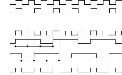
180 |
Chapter 8 |
clk outp
(a)
clk |
|
|
out1 |
|
|
st1 |
st2 |
st3 |
out2 |
|
|
st1 |
st2 |
st3 |
outp |
|
|
(b)
Figure 8.12
Waveforms of example 8.6: (a) signal outp to be generated from clk and (b) intermediate signals out1 and out2 (outp ¼ out1 AND out2).
13----- Lower section of machine #1: ---
14PROCESS(clk)
15BEGIN
16IF (clk'EVENT AND clk='1') THEN
17pr_state1 <= nx_state1;
18END IF;
19END PROCESS;
20----- Lower section of machine #2: ---
21PROCESS(clk)
22BEGIN
23IF (clk'EVENT AND clk='0') THEN
24pr_state2 <= nx_state2;
25END IF;
26END PROCESS;
27---- Upper section of machine #1: -----
28PROCESS (pr_state1)
29BEGIN
TLFeBOOK
State Machines |
181 |
30CASE pr_state1 IS
31WHEN one =>
32out1 <= '0';
33nx_state1 <= two;
34WHEN two =>
35out1 <= '1';
36nx_state1 <= three;
37WHEN three =>
38out1 <= '1';
39nx_state1 <= one;
40END CASE;
41END PROCESS;
42---- Upper section of machine #2: -----
43PROCESS (pr_state2)
44BEGIN
45CASE pr_state2 IS
46WHEN one =>
47out2 <= '1';
48nx_state2 <= two;
49WHEN two =>
50out2 <= '0';
51nx_state2 <= three;
52WHEN three =>
53out2 <= '1';
54nx_state2 <= one;
55END CASE;
56END PROCESS;
57outp <= out1 AND out2;
58END fsm;
59------------------------------------------
Simulation results from the circuit synthesized with the code above are shown in figure 8.13.
8.4Encoding Style: From Binary to OneHot
To encode the states of a state machine, we can select one among several available styles. The default style is binary. Its advantage is that it requires the least number of
TLFeBOOK

182 |
Chapter 8 |
Figure 8.13
Simulation results of example 8.6.
Table 8.1
State encoding of an 8-state FSM.
|
Encoding Style |
|
|
|
|
|
|
STATE |
BINARY |
TWOHOT |
ONEHOT |
|
|
|
|
state0 |
000 |
00011 |
00000001 |
state1 |
001 |
00101 |
00000010 |
state2 |
010 |
01001 |
00000100 |
state3 |
011 |
10001 |
00001000 |
state4 |
100 |
00110 |
00010000 |
state5 |
101 |
01010 |
00100000 |
state6 |
110 |
10010 |
01000000 |
state7 |
111 |
01100 |
10000000 |
|
|
|
|
flip-flops. In this case, with n flip-flops (n bits), up to 2n states can be encoded. The disadvantage of this encoding scheme is that it requires more logic and is slower than the others.
At the other extreme is the onehot encoding style, which uses one flip-flop per state. Therefore, it demands the largest number of flip-flops. In this case, with n flip-flops (n bits), only n states can be encoded. On the other hand, this approach requires the least amount of extra logic and is the fastest.
An style that is inbetween the two styles above is the twohot encoding scheme, which presents two bits active per state. Therefore, with n flip-flops (n bits), up to n(n 1)/2 states can be encoded.
The onehot style is recommended in applications where flip-flops are abundant, like in FPGAs (Field Programmable Gate Arrays). On the other hand, in ASICs (Application Specific Integrated Circuits) the binary style is generally preferred.
As an example, say that our state machine has eight states. Then the encoding would be that shown table 8.1. The number of flip-flops required in each case is three (for binary), five (twohot), or eight (onehot). Other details are also presented in the table.
TLFeBOOK

State Machines |
183 |
|
rst |
inp=0 |
|
inp |
state1 |
inp=1 |
state2 |
(outp=00) |
|
(outp=01) |
|
|
inp=1 |
inp=0 |
inp=0 |
|
|
||
|
|
|
|
|
|
|
inp=1 |
|
state4 |
|
state3 |
|
(outp=11) |
|
(outp=10) |
inp=1 |
inp=0 |
|
Figure P8.1
8.5Problems
Each solution to the problems proposed below should be accompanied by synthesis and simulation results. Verify, at least, the following: number of flip-flops inferred and circuit functionality.
Problem 8.1: FSM
Write a VHDL code that implements the FSM described by the states diagram of figure P8.1.
Problem 8.2: Signal Generator #1
Using the FSM approach, design a circuit capable of generating the two signals depicted in figure P8.2 (out1, out2) from a clock signal clk. The signals are periodic and have the same period. However, while one changes only at the rising edge of clk, the other has changes at both edges.
Problem 8.3: Signal Generator #2
Design a finite state machine capable of generating two signals, UP and DOWN, as illustrated in figure P8.3. These signals are controlled by two inputs, GO and STOP. When GO changes from ‘0’ to ‘1’, the output UP must go to ‘1’ too, but T ¼ 10 ms later. If GO returns to ‘0’, then UP must return to ‘0’ immediately. However, the output DOWN must now go to ‘1’, again 10 ms later, returning to ‘0’ immediately if
TLFeBOOK
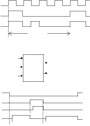
184 |
Chapter 8 |
clk
out1
out2
1 period
Figure P8.2
GO
STOP |
|
Signal |
|
UP |
|
||||
|
Generator |
|
|
|
|
|
|
||
|
|
|
|
DOWN
clk
STOP
GO
UP
 T
T
DOWN
T |
T |
Figure P8.3
GO changes to ‘1’. If the input STOP is asserted, then both outputs must go to ‘0’ immediately and unconditionally. Assume that a 10 kHz clock is available.
Problem 8.4: Keypad Debouncer and Encoder
Consider the keypad shown in the diagram of figure P8.4. A common way of reading a key press is by means of a technique called scanning or polling, which reduces the number of wires needed to interconnect the keypad to the main circuit. It consists of sending one column low at a time, while reading each row sequentially. If a key is pressed, then the corresponding row will be low, while the others remain high (due to the pull-up resistors).
TLFeBOOK

State Machines |
185 |
VDD
|
|
|
|
|
|
|
|
|
|
|
|
|
inp1 |
data6 |
1 |
|
2 |
|
3 |
|
|
|
|
|
|
|
|
||
|
|
|
|
|
|
|
|
|
|
|
|
|
|
... |
|
|
|
|
|
|
|
|
|
|
|
|
|
|
|
4 |
|
5 |
|
6 |
|
|
|
|
|
|
|
|
inp2 |
data1 |
|
|
|
|
|
|
|
|
|
|
|
|
|
inp3 |
data0 |
|
|
|
|
|
|
|
|
|
|
|
|
|
||
|
|
|
|
|
|
|
|
|
|
|
|
|
||
7 |
|
8 |
|
9 |
|
|
|
|
|
|
|
|
new_data |
|
|
|
|
|
|
|
|
|
|
|
|
|
|
|
|
|
|
|
|
|
|
|
|
|
|
|
|
|
|
* |
0 |
# |
inp4 |
outp2 |
|
||||
|
|
|
|
outp1 |
|
|
|
|
outp0 |
outp |
inp |
digit |
data |
|
|
|
ASCII |
011 |
0111 |
1 |
31h |
|
1011 |
4 |
34h |
|
1101 |
7 |
37h |
|
1110 |
* |
2Ah |
101 |
0111 |
2 |
32h |
|
1011 |
5 |
35h |
|
1101 |
8 |
38h |
|
1110 |
0 |
30h |
110 |
0111 |
3 |
33h |
|
1011 |
6 |
36h |
|
1101 |
9 |
39h |
|
1110 |
# |
23h |
Figure P8.4
TLFeBOOK
186 |
Chapter 8 |
Encoding: Each digit must be encoded using the ASCII code (7 bits, with the corresponding hexadecimal values listed in the table of figure P8.4). When a new reading is available at the output, the new_data bit should be set to ‘1’. This will avoid interpreting a key pressed for a long time as a long series of the same character.
Debouncing: A problem inherent to mechanical switches is switch bounces, which occur before a firm contact is finally established. The settling generally takes up to a few milliseconds. Therefore, the choice of the clock frequency is very important. You are asked to choose it such that at least three readings occur in a 5 ms interval. Thus the new_data bit should be turned high only when the same result is obtained in all consecutive readings within a 5 ms interval.
Problem 8.5: Tra‰c Light Controller
Using your synthesis tool plus a CPLD/FPGA development kit, implement the TLC of example 8.5. Verify, in the report files generated by your software, which pins of the chip were assigned to the inputs (clk, stby, test) and to the outputs (r1, y1, g1, r2, y2, g2). Then make the following physical connections in your board:
a 60 Hz square wave signal (from a signal generator), with the appropriate logic levels, to the clk pin.
a VDD/GND switch to pin stby.
a VDD/GND switch to pin test.
an LED (red, if possible), with a 330-1kohm series resistor, to pin r1 (resistor connected between r1 and the anode of the LED, and cathode connected to GND).
an LED (yellow, if possible) to pin y1, with a series resistor like above.
an LED (green, if possible) to pin g1, with a series resistor like above.
finally, install other 3 LEDs, like those above, for r2, y2, and g2.
Now download the program file from your PC to the development kit and verify the operation of the TLC. Play with the switches in order to test all modes of operation. You can also increase the clock frequency to speed up the transition from red to yellow, etc.
Problem 8.6: Signal Generator #3
Solve problem 8.2 without using the finite state machine approach.
Problem 8.7: Signal Generator #4
Solve example 8.6 without using the FSM approach.
For further work is this area, see problems 9.3, 9.4, and 9.6 of chapter 9.
TLFeBOOK